Transmission Electron Microscopy (TEM) Prof.Dr.Figen KAYA
|
|
|
- Gervais Bond
- 6 years ago
- Views:
Transcription
1 Transmission Electron Microscopy (TEM) Prof.Dr.Figen KAYA
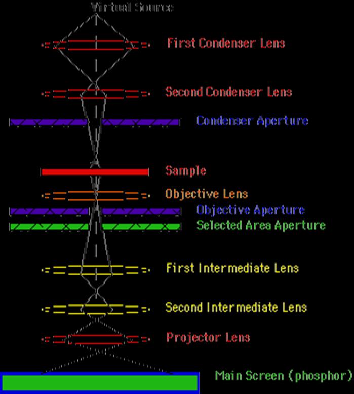
2 Transmission Electron Microscope A transmission electron microscope, similar to a transmission light microscope, has the following components along its optical path: light source, condenser lens, specimen stage, Objective lens and Projector lens as shown in Figure 3.1.
3
4
5 Instrumentation The main differences are that, in a TEM, the visible light ray is replaced by an electron ray and glass lenses are replaced by electromagnetic lens for the electron beam. The TEM has more lenses (the intermediate lens) and more apertures (including the selected area aperture).
6 Instrumentation The TEM contains further features arising from using electrons as illumination. High Vacuum: For example, a vacuum environment is required in a TEM because collisions between high energy electrons and air molecules significantly absorb electron energy.

7 Transmission Electron Microscope/ Transmission Light Microscope Table 3.1 provides a comparison of a TEM with a light microscope.

8 TEM versus Optical Microscopy
9 cs/microscopes/tem/tem.html ion_of_condenser_system.htm#
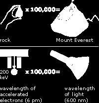
10 Electron Sources In a TEM system, an electron gun generates a high energy electron beam for illumination. In the electron gun, the electrons emitted from a cathode, a solid surface, are accelerated by high voltage (Vo) to form a high energy electron beam with energy. Because electron energy determines the wavelength of electrons and wavelength largely determines resolution of the microscope, the acceleration voltage determines the resolution to a large extent.
11 V o and Wavelength Table 3.2 gives the relationship between the acceleration voltage and wavelength.
12 Resolution in TEM To achieve a high resolution, the TEM is usually operated under an acceleration voltage of greater than 100 kv. In practice, 200 kv is commonly used and meets most resolution requirements. High-voltage electron microscopy ( 1000 kv) requires extremely expensive instrumentation, and also it may damage a specimen by generating microstructural defects in it during observation.
13 Condenser Lenses in TEM The lens system of a TEM is more complicated than a light microscope. There are two or more condenser lenses to demagnify the electron beam emitted from the electron gun. The condenser lens system controls the beam diameter and convergence angles of the beam incident on a specimen. During operation, the illumination area of specimen and illumination intensity can be adjusted by controlling the current in the electromagnetic lenses of condensers.

14 Objective lens The objective lens forms an inverted initial image, which is subsequently magnified. In the back focal plane of the objective lens a diffraction pattern is formed. The objective aperture can be inserted here. The objective lens would not usually provide a magnification of more than 50 and a TEM is routinely used to view regions of the specimen which are only a mm or so across.
15 Intermediate Lens The intermediate lens is used to switch the TEM between an image mode and a diffraction mode. For the image mode: The intermediate lens is focused on the image plane of the objective lens, For the diffraction mode: The intermediate lens is focused on the back-focal plane of the objective lens where the diffraction pattern forms.
16
17 Projector Lens The projector lens further magnifies the image or diffraction pattern and projects it onto the fluorescent screen for observation or the photographic plane. Magnification in the electron microscope can be varied from hundreds to several hundred thousands of times. This is done by varying the strength of the projector and intermediate lenses. Not all lenses will necessarily be used at lower magnifications.
18 0,4 mm 0,02 mm Objective Lens X50 Intermediate Lens 0,4 mm X20 1 st Projector Lens 8 mm X20 2 nd Projector Lens 200 mm X25 Total Magnification=50*20*20*25= X500000
19 0,4 mm Objective Lens 0,02 mm X50 Intermediate Lens 0,2 mm X10 1 st Projector Lens 2 nd Projector Lens 2 mm X10 Total Magnification=50*10*10= X5000
20 0,4 mm Objective Lens 0,02 mm X50 Intermediate Lens 0,4 mm X20 1 st Projector Lens 8 mm 400 mm X20 2 nd Projector Lens X50 Total Magnification=50*20*20*50= X

21 Specimen Stage The TEM has special requirements for specimens to be examined. TEM specimens must be a thin foil because they should be able to transmit electrons; that is, they are electronically transparent. A thin specimen is mounted in a specimen holder, as shown in Figure 3.6, in order to be inserted into the TEM column for observation.

22 TEM Specimens The holder requires that a specimen is a 3-mm disc. Smaller specimens can be mounted on a 3-mm mesh disc as illustrated in Figure 3.7. The meshes, usually made from copper, prevent the specimens from falling into the TEM vacuum column. Also, a copper mesh can be coated with a thin film of amorphous carbon in order to hold specimen pieces even smaller than the mesh size.
23 Specimen Preparation Preparation of specimens often is the most tedious step in TEM examination. To be electronically transparent, the material thickness is limited. We have to prepare a specimen with at least part of its thickness at about 100 nm, depending on the atomic weight of specimen materials. For higher atomic weight material, the specimen should be thinner. A common procedure for TEM specimen preparation is described as follows.
24 Pre-Thinning Pre-thinning is the process of reducing the specimen thickness to about 0.1mm before final thinning to 100 nm thickness. First, a specimen less than 1mm thick is prepared. This is usually done by mechanical means, such as cutting with a diamond saw. Then, a 3-mm-diameter disc is cut with a specially designed punch before further reduction of thickness.
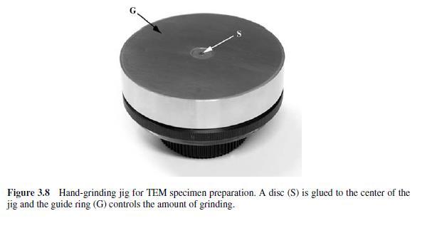
25 Grinding Grinding is the most commonly used technique to reduce the thickness of metal and ceramic specimens. During grinding, we should reduce thickness by grinding both sides of a disc, ensuring the planes are parallel. This task would be difficult without special tool. Figure 3.8 shows a hand-grinding jig for prethinning. The disc (S) is glued to the central post and a guard ring (G) guides the grinding thickness.
26
27 Dimple grinder A dimple grinder is also used for pre-thinning, particularly for specimens that are finally thinned by ion milling.
28 Final Thinning Three methods of final thinning are described here: 1. Electrolytic thinning for metal specimens that are good electric conductors, 2. Ion milling for metal and ceramic specimens, and 3. Ultramicrotome cutting for polymeric and biological specimens.
29 Electrolytic Thinning Electrolytic thinning and ion milling are methods for reducing specimen thickness to the scale of 100 nm. These methods create a dimpled area on prethinned specimens because it is almost impossible to reduce the thickness of specimens uniformly to the level of electron transparency. The dimpled area is likely to have regions of electron transparency as schematically shown in Figure 3.9.
30
31 Electrolytic thinning Electrolytic thinning is widely used for preparing specimens of conducting materials. A specimen is placed in an electrochemical cell with the specimen as anode. A suitable electrolyte (usually an acidic solution) is used to electrochemically reduce specimen thickness. A common technique is jet polishing, illustrated schematically in Figure 3.10.
32
33 Electrolytic thinning A specimen is placed in a holder with two sides facing guides of electrolyte jet streams, which serve as cathode. The electrolyte jet polishes both sides of the specimen until light transparency is detected by a light detector. Catching the precise moment that tiny holes appear is crucial, because only the edge of a tiny hole contains thin sections of electron transparency. Electrolytic thinning is very efficient and is completed in only 3 15 minutes.
34 Ion Milling Ion milling uses a beam of energetic ions to bombard specimen surfaces in order to reduce the thickness by knocking atoms out of a specimen. The specimen does not need to be electrically conductive for ion milling. Thus, the technique is suitable for metal, ceramics and other materials, as long as they are thermally stable.
35 Ion Milling Figure 3.11 illustrates the general procedure of ion milling. Before ion milling, the specimen is often ground with a dimple grinding device in order to reduce the thickness in the central are of specimen (Figure 3.11a). Then, the ground specimen is cut as a 3-mm disc and placed in the ion milling chamber with a geometric arrangement as shown in Figure 3.11b.
36 Figure 3.11 Ion thinning process: (a) dimple grinding; and (b) ion milling.
37 Ion Milling The edge of the specimen disc may need to be covered by a molybdenum ring in order to strengthen it during ion milling. An ion beam with energy of 1 10 kev bombards the specimen. The specimen is placed in the center at an angle of about 5 30 to the ion beam in order have a high yield of sputtering. Light transparency is detected by a light detector aligned along the vertical direction.
38 Ion Milling The ion beam can raise the temperature of the specimen rapidly and dramatically. Thus, cooling the chamber with liquid nitrogen is necessary in order to prevent specimen heating by the ion beam. Even with cooling, organic materials are not suitable for ion milling because the ion beam can cause severe damage to the microstructure of organic specimens such as polymers.
39 Ultramicrotomy Ultramicrotomy is basically the same type of method as microtomy for preparing soft specimens for light microscopy. However, ultramicrotomy can be used to section a specimen to the 100 nm scale. It is commonly used to prepare polymeric or biological TEM specimens.
40 Ultramicrotomy Figure 3.12 illustrates the working principles of the instrument. A specimen is mounted in a holder against the cutting tool (glass knife or diamond knife). The specimen should be trimmed to have a tip held against the knife. The cross-section of the trimmed tip usually is only about 1mm 2 for diamond knife cutting. The holder gradually moves toward the knife while it repeatedly moves up and down. The firmly mounted specimen is sectioned as it passes the edge of the knife blade.
41
42 Ultramicrotomy To be sectioned by an ultramicrotome, materials must be softer than the knife. Even though diamond is the hardest material available, a specimen can still damage the tip of a diamond knife because the extremely sharp tip of a diamond knife makes it very fragile.
43 Image Modes Contrast in transmission light microscopy is generated by differences in light absorption in different regions of the specimen. In TEM, however, absorption of electrons plays a very minor role in image formation.
44 Image Modes TEM contrast relies instead on deflection of electrons from their primary transmission direction when they pass through the specimen.
45 Imaging Modes The contrast is generated when there is a difference in the number of electrons being scattered away from the transmitted beam. There are two mechanisms by which electron scattering creates images: 1. Mass-density contrast and 2. Diffraction contrast.
46 Mass-Density Contrast The deflection of electrons can result from interaction between electrons and an atomic nucleus. Deflection of an electron by an atomic nucleus, which has much more mass than an electron, is like a collision between a particle and a wall.
47 Mass-Density Contrast The particle (electron) changes its path after collision. The amount of electron scattering at any specific point in a specimen depends on the mass-density (product of density and thickness) at that point.
48 Mass-Density Contrast Thus, difference in thickness and density in a specimen will generate variation in electron intensity received by an image screen in the TEM, if we only allow the transmitted beam to pass the objective aperture as shown in Figure 3.13.
49 Mass-Density Contrast The deflected electron with scattering angle larger than the α angle controlled by the objective aperture will be blocked by the aperture ring. Thus, the aperture reduces the intensity of the transmission beam as the beam passes through it.
50 The brightness of the image is determined by the intensity of the electron beam leaving the lower surface of the specimen and passing through the objective aperture.
51 Williams and Carter, TEM, Part 3 Springer 2009
52 Contrast Formation by Mass-Density The intensity of the transmitted beam (I t ) is the intensity of primary beam (I o ) minus the intensity of beam deflected by object (I d ) in a specimen.
53 Contrast Formation by Mass-Density This type of mass density contrast exists in all types of materials. It is the main mechanism for image formation for non-crystalline materials such as amorphous polymers and biological specimens. The mass-density contrast is also described as absorption contrast, which is rather misleading because there is little electron absorption by the specimen.
 and")
54 Figure 3.14 TEM image of polymer blend containing polycarbonate (PC) and polybutylene terephthalate (PBT) with mass-density contrast.


55 Diffraction Contrast We can also generate contrast in the TEM by a diffraction method. Diffraction contrast is the primary mechanism of TEM image formation in crystalline specimens. Diffraction can be regarded as collective deflection of electrons.
56 Diffraction Contrast Electrons can be scattered collaboratively by parallel crystal planes. Bragg s Law (nλ=2sin ϴ) which applies to X-ray diffraction, also applies to electron diffraction.
57
58 Diffraction Contrast When the Bragg conditions are satisfied at certain angles between electron beams and crystal orientation, constructive diffraction occurs and strong electron deflection in a specimen results, as schematically illustrated in Figure 3.15.

59 Crystalline Materials and Crystal Planes
60 Diffraction Contrast Thus, the intensity of the transmitted beam is reduced when the objective aperture blocks the diffraction beams, similar to the situation of massdensity contrast.
61 Diffraction Contrast
62 nλ= 2dsinθ
63 Bright Field and Dark Field Imaging in TEM The diffraction contrast can generate bright-field and dark-field TEM images. In order to understand the formation of brightfield and dark-field images, the diffraction mode in a TEM must be mentioned. A TEM can be operated in two modes: the image mode and the diffraction mode.
64 Figure 3.15 Electron deflection by Bragg diffraction of a crystalline specimen: (a) image formation in crystalline samples; and (b) diffraction at crystal lattice planes and at the contours of inclusions.
65 Bright Field and Dark Field Imaging in TEM A bright-field image is obtained by allowing only the transmitted beam to pass the objective aperture, exactly the same as in mass-density contrast. A dark-field image, however, is obtained by allowing one diffraction beam to pass the objective aperture.
66 Bright Field and Dark Field Imaging in TEM Dark-field is not as commonly used as bright-field imaging. However, the dark-field image may reveal more fine features that are bright when the background becomes dark. Figure 3.21 shows a comparison between brightand dark-field images for the same area in an Al Fe Si alloy. The dark-field image (Figure 3.21b) reveals finer details inside the grains.

 B) Dark")
67 Bright Field/Dark Field image comparison in Al-Fe-Si Alloy a) Bright Field İmage b) B) Dark Field İmage

68 High resolution transmission electron microscope (HRTEM) image of a lead crystal between two crystals of aluminum (i.e., a Pb precipitate at a grain boundary in Al). The two crystals of Al have different orientations, evident from their different patterns of atom columns. Note the commensurate atom matching of the Pb crystal with the Al crystal at right, and incommensurate atom matching at left. An isolated Pb precipitate is seen to the right.


69 The interface between GaP and ZnSe crystals. A carbon nanotube at its end portion.


 dislocation")
70 Figure 3.47 Brightfield images of dislocations: (a) in a Al Zn Mg alloys with 3% tension strain; (b) lining up in a Ni Mo alloy; and (c) dislocation cell structure in pure Ni.
71 Diffraction patterns The appearance of the diffraction pattern can reflect the nature of the crystalline phases in the specimen. For example, if the material is microcrystalline or amorphous the diffraction pattern consists of a series of concentric rings rather than spots/discs.
72 When the electron beam interacts with the sample when the sample is oriented with a zone axis pattern parallel to the electron beam, then the diffraction pattern form in the back focal plane of the objective lens is a regular array of reflections. This is seen projected onto the viewing screen as an array of reflections organized in a predictable manner based on the crystal structure of the sample.
.")
73 PowderCell 2.0 Example: Study of unknown phase in a BiFeO 3 thin film Metal organic compound on Pt TiO 2 Pt BiFeO 3 Lim Heat treatment at 350 o C (10 min) to remove organic parts. Process repeated three times before final heat treatment at o C (20 min). (intermetallic phase grown) SiO 2 Bi Bi O Si Bi Fe O Bi Bi O O Fe Fe O 200 nm Fe O Bi Bi O Fe O Fe O Bi O Bi O Bi O Goal: Fe Fe O Bi Fe O O BiFeO 3 with space grupe: R3C and celle dimentions: a= Å c= Å b c a Fe Bi Bi Bi O Fe O Fe Bi O Bi
STUDY & ANALYSIS OF ALUMINIUM FOIL AND ANATASE TITANIUM OXIDE (TiO2) USING TRANSMISSION ELECTRON MICROSCOPY
 USING TRANSMISSION ELECTRON MICROSCOPY") STUDY & ANALYSIS OF ALUMINIUM FOIL AND ANATASE TITANIUM OXIDE (TiO2) USING TRANSMISSION ELECTRON MICROSCOPY Ayush Garg Department of Chemical and Materials Engineering, University of Auckland, Auckland,
STUDY & ANALYSIS OF ALUMINIUM FOIL AND ANATASE TITANIUM OXIDE (TiO2) USING TRANSMISSION ELECTRON MICROSCOPY Ayush Garg Department of Chemical and Materials Engineering, University of Auckland, Auckland,
Electron microscopy II
 Electron microscopy II Nanomaterials characterization I RNDr. Věra Vodičková, PhD. Interaction ction: electrons solid matter Signal types SE.secondary e - AE Auger s e - BSE back scattered e - X-ray photons,
Chapter 3 Basic Crystallography and Electron Diffraction from Crystals. Lecture 9. Chapter 3 CHEM Fall, L. Ma
 Chapter 3 Basic Crystallography and Electron Diffraction from Crystals Lecture 9 Outline The geometry of electron diffraction Crystallography Kinetic Theory of Electron diffraction Diffraction from crystals
Specimen Preparation Technique for a Microstructure Analysis Using the Focused Ion Beam Process
 Specimen Preparation Technique for a Microstructure Analysis Using the Focused Ion Beam Process by Kozue Yabusaki * and Hirokazu Sasaki * In recent years the FIB technique has been widely used for specimen
Microstructural Characterization of Materials
 Microstructural Characterization of Materials 2nd Edition DAVID BRANDON AND WAYNE D. KAPLAN Technion, Israel Institute of Technology, Israel John Wiley & Sons, Ltd Contents Preface to the Second Edition
Crystallographic Textures Measurement
 Crystallographic Textures Measurement D. V. Subramanya Sarma Department of Metallurgical and Materials Engineering Indian Institute of Technology Madras E-mail: vsarma@iitm.ac.in Macrotexture through pole
Imaging with Diffraction Contrast
 Imaging with Diffraction Contrast Duncan Alexander EPFL-CIME 1 Introduction When you study crystalline samples TEM image contrast is dominated by diffraction contrast. An objective aperture to select either
Dislocations Linear Defects
 Dislocations Linear Defects Dislocations are abrupt changes in the regular ordering of atoms, along a line (dislocation line) in the solid. They occur in high density and are very important in mechanical
Carnegie Mellon MRSEC
 Carnegie Mellon MRSEC Texture, Microstructure & Anisotropy, Fall 2009 A.D. Rollett, P. Kalu 1 ELECTRONS SEM-based TEM-based Koseel ECP EBSD SADP Kikuchi Different types of microtexture techniques for obtaining
TEM and Electron Diffraction Keith Leonard, PhD (1999) U. Cincinnati
 U. Cincinnati") TEM and Electron Diffraction Keith Leonard, PhD (1999) U. Cincinnati Electron Microscopes: Electron microscopes, such as the scanning electron microscope (SEM) and transmission electron microscope (TEM)
TEM and Electron Diffraction Keith Leonard, PhD (1999) U. Cincinnati Electron Microscopes: Electron microscopes, such as the scanning electron microscope (SEM) and transmission electron microscope (TEM)
TEM imaging and diffraction examples
 TEM imaging and diffraction examples Duncan Alexander EPFL-CIME 1 Diffraction examples Kikuchi diffraction Epitaxial relationships Polycrystalline samples Amorphous materials Contents Convergent beam electron
The principles and practice of electron microscopy
 The principles and practice of electron microscopy Second Edition Ian M. Watt CAMBRIDGE UNIVERSITY PRESS Contents Preface tofirstedition page ix Preface to second edition xi 1 Microscopy with light and
UNIVERSITY OF OSLO. Faculty of Mathematics and Natural Sciences
 Page 1 UNIVERSITY OF OSLO Faculty of Mathematics and Natural Sciences Exam in MENA3100 Characterization of materials Day of exam: 12th. June 2015 Exam hours: 14:30 This examination paper consists of 5
Transzmissziós és pásztázó elektronmikroszkópos minták készítése ionsugaras vékonyítással
 Transzmissziós és pásztázó elektronmikroszkópos minták készítése ionsugaras vékonyítással Radi Zsolt Technoorg Linda Kft., Budapest Oktatói és Doktorandusz Konferencia Visegrád, 2012 State-of-the-art materials
Practical 2P8 Transmission Electron Microscopy
 Practical 2P8 Transmission Electron Microscopy Originators: Dr. N.P. Young and Prof. J. M. Titchmarsh What you should learn from this practical Science This practical ties-in with the lecture course on
Practical 2P8 Transmission Electron Microscopy
 Practical 2P8 Transmission Electron Microscopy Originators: Dr. M. L. Jenkins and Prof. J. M. Titchmarsh What you should learn from this practical Science This practical ties-in with the lecture course
Electron Probe Micro-Analysis (EPMA)
") Electron Probe Micro-Analysis (EPMA) Nilanjan Chatterjee, Ph.D. Principal Research Scientist 1 Electron Microprobe Facility Department of Earth, Atmospheric and Planetary Sciences Massachusetts Institute
Electron Probe Micro-Analysis (EPMA) Nilanjan Chatterjee, Ph.D. Principal Research Scientist 1 Electron Microprobe Facility Department of Earth, Atmospheric and Planetary Sciences Massachusetts Institute
CHEM-E5225 :Electron Microscopy Imaging II
 CHEM-E5225 :Electron Microscopy Imaging II D.B. Williams, C.B. Carter, Transmission Electron Microscopy: A Textbook for Materials Science, Springer Science & Business Media, 2009. Z. Luo, A Practical Guide
Specimen configuration
 APPLICATIONNOTE Model 1040 NanoMill TEM specimen preparation system Specimen configuration Preparing focused ion beam (FIB) milled specimens for submission to Fischione Instruments. The Model 1040 NanoMill
Electron Microscopy. Dynamical scattering
 Electron Microscopy 4. TEM Basics: interactions, basic modes, sample preparation, Diffraction: elastic scattering theory, reciprocal space, diffraction pattern, Laue zones Diffraction phenomena Image formation:
Microstructures and dislocations in the stressed AZ91D magnesium alloys
 Materials Science and Engineering A344 (2002) 279/287 www.elsevier.com/locate/msea Microstructures and dislocations in the stressed AZ91D magnesium alloys R.M. Wang a,b,, A. Eliezer a, E. Gutman a a Ben-Gurion
Sketch the light paths from object to image in a single lens system in following situations.
 Solutions o Chapter I 1.1. There are three rules governing light path or a simple lens: 1) light ray passing through the center o a lens is not deviated. ) Light ray parallel with optic axis will pass
EMSE Weak-Beam Dark-Field Technique
 Weak-Beam Dark-Field Technique 1 Weak-Beam Dark-Field Imaging Basic Idea recall bright-field contrast of dislocations: specimen close to Bragg condition, s î 0 near the dislocation core, some planes curved
The object of this experiment is to test the de Broglie relationship for matter waves,
 Experiment #58 Electron Diffraction References Most first year texts discuss optical diffraction from gratings, Bragg s law for x-rays and electrons and the de Broglie relation. There are many appropriate
Study of Structure-Phase State of Oxide Films on E110 and E635 Alloys at Pre- and Post-Irradiation Stages
 A.A. BOCHVAR HIGH-TECHNOLOGY RESEARCH INSTITUTE OF INORGANIC MATERIALS (SC «VNIINM») 18TH INTERNATIONAL SYMPOSIUM ON ZIRCONIUM IN THE NUCLEAR INDUSTRY «ROSATOM» STATE ATOMIC ENERGY CORPORATION MAY 15-19,
EBSD Basics EBSD. Marco Cantoni 021/ Centre Interdisciplinaire de Microscopie Electronique CIME. Phosphor Screen. Pole piece.
 EBSD Marco Cantoni 021/693.48.16 Centre Interdisciplinaire de Microscopie Electronique CIME EBSD Basics Quantitative, general microstructural characterization in the SEM Orientation measurements, phase
JSM-7800F Field Emission Scanning Electron Microscope
 JSM-7800F catalogue JSM-7800F Field Emission Scanning Electron Microscope We provide high performance The Ultimate Research Tool for Multi-Disciplinary Research Institutions Extreme resolution The super
3. Solidification & Crystalline Imperfections
 3. Solidification & Crystalline Imperfections solidification (casting process) of metals divided into two steps (1) nucleation formation of stable nuclei in the melt (2) growth of nuclei into crystals
LECTURE 7. Dr. Teresa D. Golden University of North Texas Department of Chemistry
 LECTURE 7 Dr. Teresa D. Golden University of North Texas Department of Chemistry Diffraction Methods Powder Method For powders, the crystal is reduced to a very fine powder or microscopic grains. The sample,
P. N. LEBEDEV PHYSICAL INSTITUTE OF THE RUSSIAN ACADEMY OF SCIENCES PREPRINT
 P. N. LEBEDEV PHYSICAL INSTITUTE OF THE RUSSIAN ACADEMY OF SCIENCES PREPRINT 18 CHANNELING A.V. BAGULYA, O.D. DALKAROV, M.A. NEGODAEV, A.S. RUSETSKII, A.P. CHUBENKO, V.G. RALCHENKO, A.P. BOLSHAKOV EFFECT
Fundamentals of X-ray diffraction and scattering
 Fundamentals of X-ray diffraction and scattering Don Savage dsavage@wisc.edu 1231 Engineering Research Building (608) 263-0831 X-ray diffraction and X-ray scattering Involves the elastic scattering of
Growth Of TiO 2 Films By RF Magnetron Sputtering Studies On The Structural And Optical Properties
 Journal of Multidisciplinary Engineering Science and Technology (JMEST) Growth Of TiO 2 Films By RF Magnetron Sputtering Studies On The Structural And Optical Properties Ahmed K. Abbas 1, Mohammed K. Khalaf
Kinematical theory of contrast
 Kinematical theory of contrast Image interpretation in the EM the known distribution of the direct and/or diffracted beam on the lower surface of the crystal The image on the screen of an EM = the enlarged
Optical microscopy Theoretical background Galina Kubyshkina
 Optical microscopy Theoretical background Galina Kubyshkina Elektromaterial Lendava d.d., Slovenia Crystalline materials presence of a unit (cell), which is periodically repeated in space regular structure
1P1b: Introduction to Microscopy
 1P1b: Introduction to Microscopy Central to the study and characterisation of metals and many other materials is the microscope, ranging from the magnification of, say, 1 to 35 in a simple stereo binocular
SEM (SCANNING ELECTRON MICROSCOPE)
") SEM (SCANNING ELECTRON MICROSCOPE) 20823856 Özgen Buğdaycı 20824336 Elif Topçuoğlu 20823985 Yavuz Duran Hacettepe University 12.04.2012 OUTLINE Definiton of scanning electron microscope History Usage Area
SEM (SCANNING ELECTRON MICROSCOPE) 20823856 Özgen Buğdaycı 20824336 Elif Topçuoğlu 20823985 Yavuz Duran Hacettepe University 12.04.2012 OUTLINE Definiton of scanning electron microscope History Usage Area
Silver Diffusion Bonding and Layer Transfer of Lithium Niobate to Silicon
 Chapter 5 Silver Diffusion Bonding and Layer Transfer of Lithium Niobate to Silicon 5.1 Introduction In this chapter, we discuss a method of metallic bonding between two deposited silver layers. A diffusion
SECTION A. NATURAL SCIENCES TRIPOS Part IA. Friday 4 June to 4.30 MATERIALS AND MINERAL SCIENCES
 NATURAL SCIENCES TRIPOS Part IA Friday 4 June 1999 1.30 to 4.30 MATERIALS AND MINERAL SCIENCES Answer five questions; two from each of sections A and B and one from section C. Begin each answer at the
Thin Film Characterizations Using XRD The Cases of VO2 and NbTiN
 Thin Film Characterizations Using XRD The Cases of VO2 and NbTiN A thesis submitted in partial fulfillment of the requirement for the degree of Bachelor of Arts / Science in Physics from The College of
Application of Advanced Techniques for Metals Identification and Characterisation
 Application of Advanced Techniques for Metals Identification and Characterisation David N Githinji Department of Manufacturing, Industrial & Textile Engineering, Moi University, P.O Box 3900-30100, Eldoret,
Identification of Crystal Structure and Lattice Parameter. for Metal Powders Using X-ray Diffraction. Eman Mousa Alhajji
 Identification of Crystal Structure and Lattice Parameter for Metal Powders Using X-ray Diffraction Eman Mousa Alhajji North Carolina State University Department of Materials Science and Engineering MSE
Lecture C4b Microscopic to Macroscopic, Part 4: X-Ray Diffraction and Crystal Packing
 Lecture C4b Microscopic to Macroscopic, Part 4: X-Ray Diffraction and Crystal Packing X-ray Diffraction Max von Laue won the 1914 Nobel Prize for his discovery of the diffraction of x-rays by crystals.
MODEL NanoMill TEM Specimen Preparation System. Ultra-low-energy, inert-gas ion source. Concentrated ion beam with scanning capabilities
 MODEL 1040 NanoMill TEM Specimen Preparation System The NanoMill system uses an ultra-low energy, concentrated ion beam to produce the highest quality specimens for transmission electron microscopy. Ultra-low-energy,
Observation in the GB (Gentle Beam) Capabilities
 Capabilities") A field-emission cathode in the electron gun of a scanning electron microscope provides narrower probing beams at low as well as high electron energy, resulting in both improved spatial resolution and
A field-emission cathode in the electron gun of a scanning electron microscope provides narrower probing beams at low as well as high electron energy, resulting in both improved spatial resolution and
Diffraction Going further
 Diffraction Going further Duncan Alexander! EPFL-CIME 1 Contents Higher order Laue zones (HOLZ)! Kikuchi diffraction! Convergent beam electron diffraction (CBED)! HOLZ lines in CBED! Thickness measurements!
Development of New Generation Of Coatings with Strength-Ductility Relationship, Wear, Corrosion and Hydrogen Embrittlement Resistance Beyond the
 Development of New Generation Of Coatings with Strength-Ductility Relationship, Wear, Corrosion and Hydrogen Embrittlement Resistance Beyond the Current Materials Accomplishments till date As the structural
MODEL TEM Mill. Two independently adjustable TrueFocus ion sources
 MODEL 1050 TEM Mill A state-of-the-art ion milling and polishing system. It is compact, precise, and consistently produces high-quality transmission electron microscopy (TEM) specimens with large electron
Experiment 2b X-Ray Diffraction* Optical Diffraction Experiments
 * Experiment 2b X-Ray Diffraction* Adapted from Teaching General Chemistry: A Materials Science Companion by A. B. Ellis et al.: ACS, Washington, DC (1993). Introduction Inorganic chemists, physicists,
Model TEM Mill. Tabletop precision preparation for producing high-quality TEM specimens from a wide variety of materials EXCELLENCE MAGNIFIED
 Model 1050 TEM Mill Tabletop precision preparation for producing high-quality TEM specimens from a wide variety of materials EXCELLENCE MAGNIFIED Modular design for basic instrument operation or fully
AP 5301/8301 Instrumental Methods of Analysis and Laboratory Lecture 4 Microscopy (III): Transmission Electron Microscopy (TEM)
: Transmission Electron Microscopy (TEM)") 1 AP 5301/8301 Instrumental Methods of Analysis and Laboratory Lecture 4 Microscopy (III): Transmission Electron Microscopy (TEM) Prof YU Kin Man E-mail: kinmanyu@cityu.edu.hk Tel: 3442-7813 Office: P6422
1 AP 5301/8301 Instrumental Methods of Analysis and Laboratory Lecture 4 Microscopy (III): Transmission Electron Microscopy (TEM) Prof YU Kin Man E-mail: kinmanyu@cityu.edu.hk Tel: 3442-7813 Office: P6422
Bragg diffraction using a 100ps 17.5 kev x-ray backlighter and the Bragg Diffraction Imager
 LLNL-CONF-436071 Bragg diffraction using a 100ps 17.5 kev x-ray backlighter and the Bragg Diffraction Imager B. R. Maddox, H. Park, J. Hawreliak, A. Comley, A. Elsholz, R. Van Maren, B. A. Remington, J.
Microstructural characterisation of as-deposited and reheated weld metal High Strength Steel Weld Metals
 Microstructural characterisation of as-deposited and reheated weld metal High Strength Steel Weld Metals Enda Keehan, Leif Karlsson, Mattias Thuvander, Eva-Lena Bergquist Abstract ESAB AB, Gothenburg,
Why does the growth rate slow down as a precipitate thickens during diffusion-controlled growth?
 Part II: Worked Examples H. K. D. H. Bhadeshia Question 14 Why does the growth rate slow down as a precipitate thickens during diffusion-controlled growth? The surface of a metal can be nitrided to form
The application of scanning electron beam anomalous transmission patterns in mineralogy
 MINERALOGICAL MAGAZINE, JUNE 1969, VOL. 37, NO. 286 The application of scanning electron beam anomalous transmission patterns in mineralogy M. P. JONES, B.SC., D.I.C., A.M.I.M.M., AND J. GAVRILOVIC, PH.D.,
TEM imaging and diffraction examples
 TEM imaging and diffraction examples Duncan Alexander EPFL-CIME 1 Diffraction examples Kikuchi diffraction Epitaxial relationships Polycrystalline samples Amorphous materials Contents Convergent beam electron
MODEL 1051 TEM Mill ION MILLING. Ion milling is used on physical science. specimens to reduce thickness to electron
 MODEL 1051 TEM Mill A state-of-the-art ion milling and polishing system offering reliable, high performance specimen preparation. It is compact, precise, and consistently produces high-quality transmission
High Resolution X-ray Diffraction
 High Resolution X-ray Diffraction Nina Heinig with data from Dr. Zhihao Donovan Chen, Panalytical and slides from Colorado State University Outline Watlab s new tool: Panalytical MRD system Techniques:
ATTACHMENTES FOR APD 2000 PRO POWDER X-RAY DIFFRACTOMETER. Monochromators
 Monochromators Secondary graphite monochromator Johansson Ka 1 monochromator Parabolic monochromator Secondary flat and curved graphite monochromators suitable for Ag, Cr, Fe, Cu, Co and Mo radiations
SPECIMEN PREPARATION FOR ELECTRON MICROSCOPY
 SPECIMEN PREPARATION FOR ELECTRON MICROSCOPY Samar Das Scientist National Metallurgical Laboratory Jamshedpur - 831 007 The purpose of electron microscopy is to study accurately the microstructures at
ECE 440 Lecture 27 : Equilibrium P-N Junctions I Class Outline:
 ECE 440 Lecture 27 : Equilibrium P-N Junctions I Class Outline: Fabrication of p-n junctions Contact Potential Things you should know when you leave Key Questions What are the necessary steps to fabricate
Supplementary Materials for
 advances.sciencemag.org/cgi/content/full/4/8/eaat4712/dc1 Supplementary Materials for In situ manipulation and switching of dislocations in bilayer graphene Peter Schweizer, Christian Dolle, Erdmann Spiecker*
Supplementary Material
 Supplementary Material Self-patterning Gd nano-fibers in Mg-Gd alloys Yangxin Li 1,2, Jian Wang 3, Kaiguo Chen 4, Meiyue Shao 2, Yao Shen 1 *, Li Jin 2 *, Guozhen Zhu 1 * 1 State Key Laboratory of Metal
9/29/2014 8:52 PM. Chapter 3. The structure of crystalline solids. Dr. Mohammad Abuhaiba, PE
 1 Chapter 3 The structure of crystalline solids 2 Home Work Assignments HW 1 2, 7, 12, 17, 22, 29, 34, 39, 44, 48, 53, 58, 63 Due Sunday 12/10/2014 Quiz # 1 will be held on Monday 13/10/2014 at 11:00 am
Lecture C4a Microscopic to Macroscopic, Part 4: X-Ray Diffraction and Crystal Packing
 Lecture C4a Microscopic to Macroscopic, Part 4: X-Ray Diffraction and Crystal Packing X-ray Diffraction Max von Laue won the 1914 Nobel Prize for his discovery of the diffraction of x-rays by crystals.
INGE Engineering Materials. Chapter 3 (cont.)
") Some techniques used: Chapter 3 (cont.) This section will address the question how do we determine the crystal structure of a solid sample? Electron microscopy (by direct and indirect observations) Scanning
Some techniques used: Chapter 3 (cont.) This section will address the question how do we determine the crystal structure of a solid sample? Electron microscopy (by direct and indirect observations) Scanning
9/28/2013 9:26 PM. Chapter 3. The structure of crystalline solids. Dr. Mohammad Abuhaiba, PE
 Chapter 3 The structure of crystalline solids 1 2 Why study the structure of crystalline solids? Properties of some materials are directly related to their crystal structure. Significant property differences
Nanoscale Imaging, Material Removal and Deposition for Fabrication of Cutting-edge Semiconductor Devices
 Hitachi Review Vol. 65 (2016), No. 7 233 Featured Articles Nanoscale Imaging, Material Removal and Deposition for Fabrication of Cutting-edge Semiconductor Devices Ion-beam-based Photomask Defect Repair
Sr and Pb additions. L. Affleck, C. Leach *
 Microstructures of BaTiO 3 based PTC thermistors with Ca, Sr and Pb additions Abstract L. Affleck, C. Leach * Manchester Materials Science Centre University of Manchester and UMIST Grosvenor Street, Manchester
Visualization of Nano-precipitate in Low-alloy Steel by Using Energy-filtered Transmission Electron Microscopy
 UDC 620. 186. 1 : 620. 187 Visualization of Nano-precipitate in Low-alloy Steel by Using Energy-filtered Transmission Electron Microscopy Yoichi IKEMATSU* 1 Genichi SHIGESATO* 1 Masaaki SUGIYAMA* 1 Abstract
Introduction to Lithography
 Introduction to Lithography G. D. Hutcheson, et al., Scientific American, 290, 76 (2004). Moore s Law Intel Co-Founder Gordon E. Moore Cramming More Components Onto Integrated Circuits Author: Gordon E.
In Situ Observation of Dislocation Nucleation and Escape in a Submicron Al Single Crystal
 Supplementary Information for In Situ Observation of Dislocation Nucleation and Escape in a Submicron Al Single Crystal Sang Ho Oh*, Marc Legros, Daniel Kiener and Gerhard Dehm *To whom correspondence
Physics and Material Science of Semiconductor Nanostructures
 Physics and Material Science of Semiconductor Nanostructures PHYS 570P Prof. Oana Malis Email: omalis@purdue.edu Today Bulk semiconductor growth Single crystal techniques Nanostructure fabrication Epitaxial
Defect and chemical analysis in the TEM
 THE UNIVERSITY Defect and chemical analysis in the TEM Defect and chemical analysis in the TEM I.P. Jones. Chemical analysis: EDX. Chemical analysis: PEELS Centre for Electron Microscopy OF BIRMINGHAM
Lesson 1 X-rays & Diffraction
 Lesson 1 X-rays & Diffraction Nicola Döbelin RMS Foundation, Bettlach, Switzerland February 11 14, 2013, Riga, Latvia Electromagnetic Spectrum X rays: Wavelength λ: 0.01 10 nm Energy: 100 ev 100 kev Interatomic
Conventional TEM. N o r t h w e s t e r n U n i v e r s i t y - M a t e r i a l s S c i e n c e
 Conventional TEM STEM N o r t h w e s t e r n U n i v e r s i t y - M a t e r i a l s S c i e n c e Reciprocity 1 1 C CCCCCCCC(2ππππππ. rr) CCCCCC(2ππππππ. rr) Reciprocity 2 1 C+D CC(gg)CCCCCC(2ππππππ.
Physics 6180: Graduate Physics Laboratory. Experiment CM5: X-ray diffraction and crystal structures
 Physics 6180: Graduate Physics Laboratory Experiment CM5: X-ray diffraction and crystal structures References: Preston and Dietz, Expt. 10 pp. 180-197 Eisberg and Resnick, Quantum Physics, Sec. 9 Kittel,
needed for the SOFC electrolyte membrane application. Few directed vapor deposition
 Chapter 3 Experimental Procedure 3.1 Overview Prior to this study, DVD has not been used to create the type of dense metal oxide layers needed for the SOFC electrolyte membrane application. Few directed
Materials Lab 1(MT344) X-ray Diffractometer Operation and Data Analysis. Instructor: Dr. Xueyan Wu ( 吴雪艳 )
 X-ray Diffractometer Operation and Data Analysis. Instructor: Dr. Xueyan Wu ( 吴雪艳 )") Materials Lab 1(MT344) X-ray Diffractometer Operation and Data Analysis Instructor: Dr. Xueyan Wu ( 吴雪艳 ) Goals To give students a practical introduction into the use of X-ray diffractometer and data collection.
Materials Lab 1(MT344) X-ray Diffractometer Operation and Data Analysis Instructor: Dr. Xueyan Wu ( 吴雪艳 ) Goals To give students a practical introduction into the use of X-ray diffractometer and data collection.
Transmission Kikuchi Diffraction in the Scanning Electron Microscope
 Transmission Kikuchi Diffraction in the Scanning Electron Microscope Robert Keller, Roy Geiss, Katherine Rice National Institute of Standards and Technology Nanoscale Reliability Group Boulder, Colorado
Properties of Materials
 Properties of Materials Thermal Properties Thermal Conductivity Temperature Wall The Thermal Conductivity (k) is the measure of the ability of a material to transmit heat by conduction. The heat (Q) is
AP 5301/8301 LABORATORY MANUAL
 AP 5301/8301 LABORATORY MANUAL Department of Physics & Materials Science City University of Hong Kong Contents Table of Contents. 1 Project 1: Scanning Electron Microscopy (SEM). 2 Project 2: Microscopic
Chapter 3: Powders Production and Characterization
 Chapter 3: Powders Production and Characterization Course Objective... To introduce selective powder production processes and characterization methods. This course will help you : To understand properties
MODEL PicoMill TEM specimen preparation system. Achieve ultimate specimen quality free from amorphous and implanted layers
 MODEL 1080 PicoMill TEM specimen preparation system Combines an ultra-low energy, inert gas ion source, and a scanning electron column with multiple detectors to yield optimal TEM specimens. POST-FIB PROCESSING
9/16/ :30 PM. Chapter 3. The structure of crystalline solids. Mohammad Suliman Abuhaiba, Ph.D., PE
 Chapter 3 The structure of crystalline solids 1 Mohammad Suliman Abuhaiba, Ph.D., PE 2 Home Work Assignments HW 1 2, 7, 12, 17, 22, 29, 34, 39, 44, 48, 53, 58, 63 Due Sunday 17/9/2015 3 Why study the structure
General Introduction to Microstructure Technology p. 1 What is Microstructure Technology? p. 1 From Microstructure Technology to Microsystems
 General Introduction to Microstructure Technology p. 1 What is Microstructure Technology? p. 1 From Microstructure Technology to Microsystems Technology p. 9 The Parallels to Microelectronics p. 15 The
ENMAT101A Engineering Materials and Processes Associate Degree of Applied Engineering (Renewable Energy Technologies) Lecture 10 Practical Microscopy
 Lecture 10 Practical Microscopy") ENMAT101A Engineering Materials and Processes Associate Degree of Applied Engineering (Renewable Energy Technologies) Lecture 10 Practical Microscopy Silicon atoms www.highered.tafensw.edu.au Metallographic
ENMAT101A Engineering Materials and Processes Associate Degree of Applied Engineering (Renewable Energy Technologies) Lecture 10 Practical Microscopy Silicon atoms www.highered.tafensw.edu.au Metallographic
Effect of Heat Treatment on Interfacial Strengthening Mechanisms of Second Phase Particulate Reinforced Aluminium Alloy
 24-26.5.2005, Hradec nad Moravici Effect of Heat Treatment on Interfacial Strengthening Mechanisms of Second Phase Particulate Reinforced Aluminium Alloy S.T. Hasan Faculty of Arts, Computing, Engineering
Analytical Methods for Materials
 Analytical Methods for Materials Lesson 4 Metallography Suggested Reading Y. Leng, Materials Characterization, 2 nd Edition, (2013), Wiley, Hoboken, NJ Chapter 1. Reference Goodhew, Humphreys and Beanland,
3D Nano-analysis Technology for Preparing and Observing Highly Integrated and Scaled-down Devices in QTAT
 Hitachi Review Vol. 54 (2005), No. 1 27 3D Nano-analysis Technology for Preparing and Observing Highly Integrated and Scaled-down Devices in QTAT Toshie Yaguchi Takeo Kamino Tsuyoshi Ohnishi Takahito Hashimoto
Signals from a thin sample
 Signals from a thin sample Auger electrons Backscattered electrons BSE Incident beam secondary electrons SE Characteristic X-rays visible light 1-100 nm absorbed electrons Specimen electron-hole pairs
Supporting Information. Solution-Processed 2D PbS Nanoplates with Residual Cu 2 S. Exhibiting Low Resistivity and High Infrared Responsivity
 Supporting Information Solution-Processed 2D PbS Nanoplates with Residual Cu 2 S Exhibiting Low Resistivity and High Infrared Responsivity Wen-Ya Wu, Sabyasachi Chakrabortty, Asim Guchhait, Gloria Yan
Materials: Structures and Synthesis
 微纳光电子材料与器件工艺原理 Materials: Structures and Synthesis Xing Sheng 盛兴 Department of Electronic Engineering Tsinghua University xingsheng@tsinghua.edu.cn 1 Optical and Electronic Devices LEDs lasers waveguides
Physical structure of matter. Monochromatization of molybdenum X-rays X-ray Physics. What you need:
 X-ray Physics Physical structure of matter Monochromatization of molybdenum X-rays What you can learn about Bremsstrahlung Characteristic radiation Energy levels Absorption Absorption edges Interference
CHAPTER 7 MICRO STRUCTURAL PROPERTIES OF CONCRETE WITH MANUFACTURED SAND
 99 CHAPTER 7 MICRO STRUCTURAL PROPERTIES OF CONCRETE WITH MANUFACTURED SAND 7.1 GENERAL Characterizing the mineralogy of the samples can be done in several ways. The SEM identifies the morphology of the
Foundations in Microbiology Seventh Edition
 Lecture PowerPoint to accompany Foundations in Microbiology Seventh Edition Talaro Chapter 3 Tools of the Laboratory: The Methods for Studying Microorganisms Copyright The McGraw-Hill Companies, Inc. Permission
IBS/e Ion Beam Sputter Deposition and Etching System. IBS/e with KDC-10 Ion Beam Sputter Deposition and Etching System with Kaufman Ion Source
 IBS/e Ion Beam Sputter Deposition and Etching System IBS/e with KDC-10 Ion Beam Sputter Deposition and Etching System with Kaufman Ion Source The Model IBS/e is a high vacuum thin film deposition system
Microscopic Structural Analysis of Advanced Anode Material for Lithium Battery
 JFE TECHNICAL REPORT No. 22 (Mar. 2017) Microscopic Structural Analysis of Advanced Anode Material for Lithium Battery SIMAUCHI Yutaka *1 OHMORI Shigekazu *2 IKEMOTO Sachi *3 Abstract: analyzed the microstructure