COFAN USA. Meeting your Project needs.
|
|
|
- Sophia Byrd
- 6 years ago
- Views:
Transcription

1 COFAN USA Meeting your Project needs
2 PCB Substrate Pre-preg Category SEKISUI Laird T-Clad Denka
3 PCB Substrate Pre-preg Category In the PCB industry, there are a couple major Pre-preg PCB materials to choose from and our team is proud to have partnerships with some of these major suppliers. Laird, Bergquist, Denka, and Sekisui are some of the industries leaders in thermally conductive PCB materials.
4 Laird The printed circuit boards (PCB) material technology is the thermally-conductive pre-preg (PP) that allows single-sided (SS) and multi-layer circuits to be made. The PP is formed into sheets in several thicknesses and is used to bond the integrated heat spreader to the circuit copper for the SS construction and two circuit copper sheets (DS) as a base for the ML constructions. There are three major applications for thermally-conductive PCB materials: power converters, motor controls, and LED lighting. Tlam thermally-conductive PCB substrates provide 8-10 times the heat dissipation compared to conventional FR4-based PCBs. The miniaturation of electronic devices continues to pack more and more power into smaller and smaller packages. The simplicity of the Tlam system takes the heat dissipation requirement in stride without significant design changes. The Tlam dielectrics are the key to these high-performance PCB substrates. The Tlam dielectric provides electrical isolation, thermal transfer, and adhesion layer for the substrates that are created for your specific needs. The Tlam system is available in a wide variety of constructions. Tlam SS is the single side PCB substrate. Tlam DS is a double-sided copper laminates and Tlam PP is the dielectrics used to bond multi-layer PCB together. The Tlam system is the most versatile thermally-enhanced PCB substrate on the Market.

5 Tlam ML 1KA Multi Layer Constructions Based on TlamDS1KA and TlamPP 1KA Tlam DS 1KA is a double sided circuit copper laminate bonded together with Tlam 1KA dielectric. Tlam DS 1KA laminates are processed through standard FR4 plate and etch operations. Tlam DS 1KA laminates are available in 6-8 mil dielectric and ounce circuit copper combinations. Tlam PP is a thick, high flow, thermally conductive pre-preg that bonds the Tlam DS board to either an aluminum or a copper base plate to complete the multi-layer insulated metal PCB (Tlam ML). Tlam PP 1KA is available in 8-12 mil thicknesses to maintain dielectric isolation on buried 4 ounce circuit copper traces. The Tlam ML based on Tlam DS 1KA and Tlam PP 1KA materials have 8-10 times better thermal conductivity compared to FR4 and this is the key to keeping components cool. The Tlam ML 1KA boards are processed through standard pick and place SMT and manual wire bond operations. FEATURESANDBENEFITS UL recognized up to 4 ounce copper internally Create cooper core IMPCB without whole fill step UL RTI of 130 C RoHS Compliant Environmentally green APPLICATIONS Multi-layer DC/DC power converters Multi-layer LED substrates

6


7
8 Tlam SS 1KA Thermally Conductive Printed Circuit Board Substrate Tlam SS 1KA is a thermally conductive printed circuit board (PCB) substrate. The substrate consists of a copper circuit layer bonded to an aluminum or copper base plate with Laird Technologies 3 watt/m-k 1KA dielectric. Tlam SS 1KA materials are processed through standard FR4 print and etch operations. Tlam SS 1KA has 8-10 times better thermal conductivity compared to FR4, and this is the key to keeping components cool. The Tlam SS 1KA boards run through standard pick and place SMT and manual wire bond processes. Tlam SS 1KA is designed for applications that require the best thermal performance and resistance to thermal cycling. Customers have found that Tlam SS 1KA reduces the stress on solder bonds with ceramic devices. Standard constructions are made with 1 and 2 ounce copper and (1 mm) and (1.6 mm) inch thick aluminum. Custom constructions of heavier weight circuit copper and thicker aluminum and copper base plates are also available. FEATURES AND BENEFITS UL 746B Electrical/Mechanical RTI as high as 130 C RoHS compliant Environmentally green Lead-free solder compatible Compliant for low bond stress APPLICATIONS Network DC/DC power converters Battery powered equipment DC/DC power converters Ultra bright LED substrates
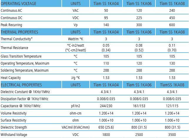
9 Tlam SS1KA Specifications
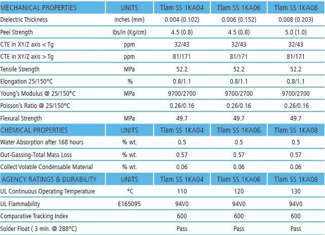
10 Tlam SS1KA Specifications
11 Tlam SS HTD Thermally Conductive Printed Circuit Board Substrate Tlam SS HTD is a thermally conductive PCB substrate. The construction consists of a copper circuit layer bonded to an aluminum or copper base plate with 150 C rated Tlam HTD dielectric. Tlam SS HTD laminate is processed through standard FR4 print and etch operations. Tlam SS HTD products have 6-8 times better thermal conductivity than FR4--key to keeping components cool. The Tlam SS HTD boards are run through standard pick and place SMT and manual wire bond processes. Tlam SS HTD is designed for use in high temperature and/or high-voltage applications typically found in industrial motor drives and automotive motor controls. Standard constructions are made with 1 and 2 ounce copper and (1mm) and (1.6mm) inch thick aluminum. Custom construction of heavier weight circuit copper and thicker aluminum and copper base plates are also available. FEATURES AND BENEFITS Lower thermal resistance UL 746 B RTI of 150 C High withstand voltage >6000 VDC RoHS compliant Environmentally green Significantly reduces power device temperature Lead free solder compatible APPLICATIONS Automotive - LV under hood and EV motor drives VAC commercial and industrial motor drives, UPS and welders Power Supplies - AC/DC and DC/DC for telecom and commercial products
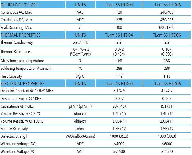
12 Tlam SS HTD Specifications
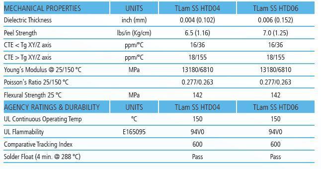
13 Tlam SS HTD Specifications
14 Tlam SS LLD Ultra-bright LED insulated Metal-Core Printed Circuit Board Material Tlam SS LLD is a copper circuit layer and aluminum or copper base plate bonded together with LLD dielectric. LLD that are processed through standard FR4 print and etch operations. LLD is designed for bright and ultra-bright LED module applications. LLD products have 6-8 times better thermal conductivity compared to FR4 and this is the key to keep components cool. LLD boards are processed through standard pick-and-place SMT and manual wire bond operations. Standard constructions are made with 1 or 2 ounce copper and (1) or (1.6) inch (mm) thick aluminum. FEATURES AND BENEFITS RoHS compliant Environmentally green Lead-free solder compatible Uses standard FR4 print and etch processing APPLICATIONS Highway and street lights using LEDs Railroad crossing signal lights using LEDs BLU for large format LCD TVs General lighting Americas: Europe: Asia: CLVcustomerservice@lairdtech.com
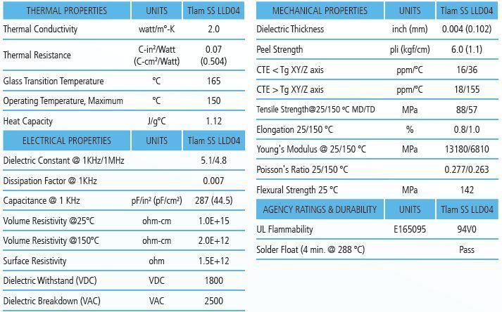
15 Tlam SSLLD Specifications
16 Bergquist Thermal Clad Insulated Metal Substrate (IMS ) was developed by Bergquist as a thermal management solution for today s higher watt-density surface mount applications where heat issues are a major concern. Thermal Clad is a cost-effective solution which can eliminate components, allow for simplified designs, smaller devices and an overall less complicated production processes. Additional benefits of Thermal Clad include lower operating temperatures, longer component life and increased durability. Bergquist Thermal Clad substrates are not limited to use with metal base layers. In one example, power conversion applications can enhance their performance by replacing FR-4 with Thermal Clad dielectrics in multi-layer assemblies. In this application, the thickness of the copper circuit layer can be minimized by the high thermal performance of Thermal Clad. Thermal Clad is a complete thermal management system, unlike traditional technology which uses heat sinks, clips and other mounting hardware. Thermal Clad enables low-cost production by eliminating the need for costly manual assembly

17 T-Clad Overview

18 T-Clad Operating Temperatures Choose the dielectric that best suits your operating temperature environment. For high temperature applications, such as automotive, HT offers the right solution. All of our dielectrics are UL recognized.


19 T-clad

20 Denka Speciation With DENKA s high value added electronic components, we accurately identify your needs and contribute to the diversification and sophistication of electronics products
21 Denka Speciation(2)

 Transient thermal resistance characteristics")
22 Denka Comparison of Thermal Conductivity a) Thermal resistance characteristics *Simulated values are used for aluminasubstrate values. b) Transient thermal resistance characteristics (20 W)


23 Denka Measuring Method used for the thermal conductivity of substrates Comparison of thermal images by thermo-viewer This photograph shows the thermal images with a 4A current applied for 10 seconds (Tr: TO-220). It can be seen that the temperature rise of the "DENKA HITT PLATE" is kept very small thanks to its excellent thermal conductivity.
24 Sekisui The world s leader in LED materials including Thermally Conductive PCB Substrate (KNDJ), Encapsulating Material (SLS), and High Reliability photo resist (SCR). Having been in the material business since 1947, this Japan based company has grown in size and capability and is one of the worlds leaders in the PCB Pre-preg field, amongst many other frontiers in the modern day and age.
25 Introduction Sekisui KNDJ

26 Features of the KNDJ Series
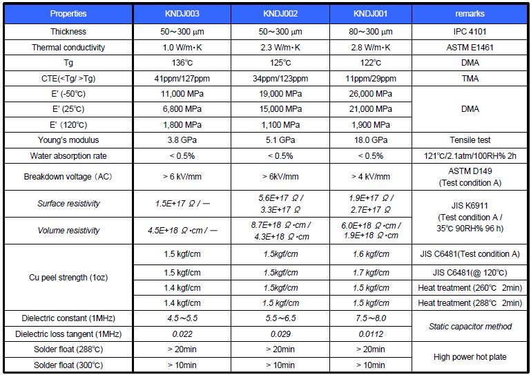
27 Sekisui KNDJ Specifications

28 Different Thermal Conductivity Measuring Methods
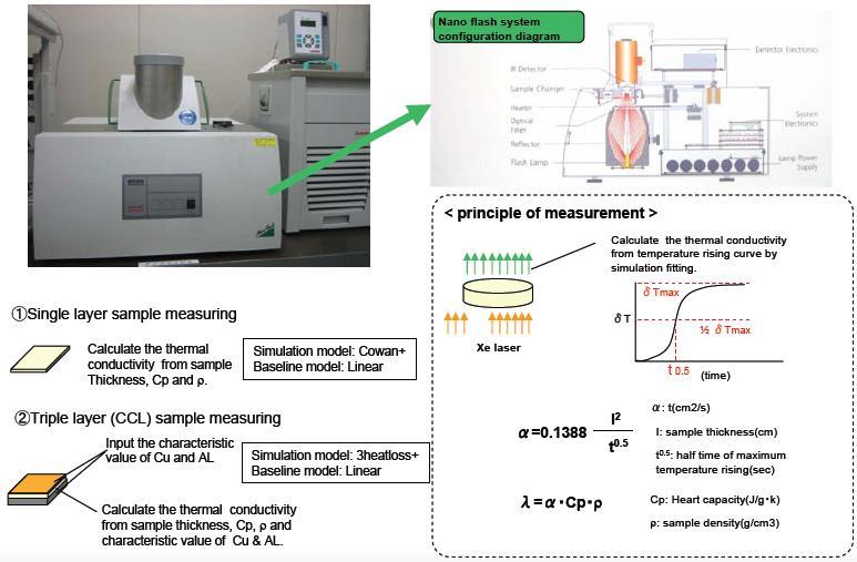
29 Nano-Flash Therm-Conductivity Test

30 Nano Flash Results

31 Heat Release Performance Test

32 Heat Release Performance Data (AL/CU)

33
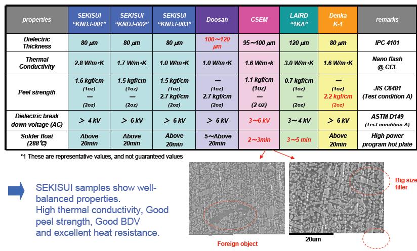
34 Comparison Table
35 Checklist FR-4 PCB Fabricated documents checklist NO. ITEM DESCRIPTION OK N/A 1 customer's specification must be provided if customer has it's spec. 2 gerber files with ZIP format : ZIP, RAR, JZIP, ARJ. (1) aperture list must be provided unless using RX-274X format (2) drawing must be provided if customer has drawing. (3) drilling program gerber format or txt. or hole chart. (4) inner layers pattern at least 2 files for 4L, 4 files for 6L, 6 files for 8L,...etc. (5) outer layers pattern at least 2 files. (6) solder mask pattern at least 2 files. (7) legend 1 or 2 files. (8) ET program may have ET program with format IPC-356 if customer has it. (9) other may have readme file if customer has it. 3 drawing dimension, tolerance, hole chart, construction, material,...etc. 4 drilling data drilling program. PTH/NPTH definition. hole quantity. 5 solder mask color. 6 legend color. 7 surface treatment OSP, HAL, Pb-free HAL, ENIG, Ni/Pd/Au, immersion Tin,...etc. 8 V-scoring web thickness & scoring angle.
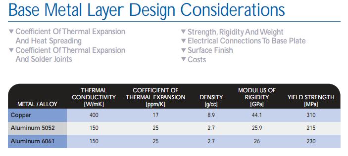
36 Process Procedure PROCESS ITEM IN HOUSE IMS nominated aluminum thickness 0.5 / 0.8 / 1.0 / 1.5 / 2.0 /3.0 mm copper foil OZ nominated panel size for Laird 18" X 24" (457 x 610 mm) dielectric thickness for Laird 4 / 6 /8 / 10 mil thermal conductive for Laird 3 W/ mk nominated panel size for sekisui 510 x 605 / 510 x 640 mm dielectric thickness for sekisui 3 mil thermal conductive for Sekisui 2 W/mk nominated layer stack 1L+pp+alu. / 2L+pp+alu. / 1L+pp+alu+pp+1L Hole drilling min hole drilling size 0.050" mm for copper, 0.040" for aluminum, general size : 0.080" max hole drilling size 0.240" ( above 0.150" using step drilling) true position +/ " PTH/Copper plating min. board thickness 0.003" Dry film min. board thickness after plating 0.006", H/H 0.003" min. board thickness before plating 0.015", H/H 0.003" min. line width/spacing see attachment resolution tolerance of line width/spacing >= 0.005" +/- 20% +/- 20% resolution tolerance of line width/spacing < 0.005" +/ " +/ " min. distnce from hole to inner trace 0.010" 0.010" registration +/ " Solder mask thickness at crest of trace 0.6 mil thickness at corner of trace 0.4 mil min width of solder dam 0.004" registration to pattern +/ "
37 Process Procedure II Legend min. stroke width 0.006" 0.006" min. distance from legend to solder pads 0.006" 0.006" registration to pattern +/ " +/ " Surface treatment (tk) HAL with sn/pb U" HAL with sn/cu/ni U" HAL with sn/ag/cu U" OSP 0.2 to 0.5 U" ENIG 100 to 300/ 1 to 8 U" immersion Ni/Pd/Au 200/4 U" electric nickel/gold plating 100 to 300/ 1 to 50 U" immersion Tin 25 to 40 U" Routing min. slot width 2 mm 2 mm min. internal radius 0.9 mm 0.9 mm dim. tolerance +/ " +/ " min. distance from copper to routing 0.5 mm 0.5 mm min. distance from slot to routing 0.5 mm 0.5 mm min. spacing between PCB 2.5 mm 2.5 mm V-Cut dim. tolerance +/ " +/ " registration upper/lower +/ " +/ " Bevelling dim. tolerance +/ " +/ " Punch dim. tolerance +/ " +/ " min. slot 0.035" 0.035" min. distance from copper to punched edge 0.5 mm min. distance from slot to punched edge 0.5 mm min. spacing from punched edge to panel edge min. slot width min. square slot see attachment of punched spec min. hole dia.
Fixed Resistors INSULATED ALUMINUM SUBSTRATES. Thermal Solutions for Hi Brightness LED Applications - Application Note
 INSULATED ALUMINUM SUBSTRATES TT electronics is a leading designer and manufacturer of electronic components. As a result of our experience with power components, Anotherm substrates were developed as
Technology Aluminium-IMS-PCBs Rev For latest information please visit
 Options and Characteristics Online calculation On explicit enquiry Quantity 1 piece up to 1,0² total area from 1 piece to mass production Layer quantity 1- and 2-layers up to 6 layers Material thickness
Insulated Metal Substrates
 Insulated Metal Substrates Presented by Les Round of Spirit Circuits ICT Evening Seminar: 15 th September 2010 Venue: Newtown Hotel, Hayling Island Why use Thermal Management The failure rate of an electronic
Manufacturing Capacity
 Capability List Manufacturing Capacity QTA & Prototype Layer : 1L ~32 L Impedance Board Ball Grid Array ( BGA ) Blind/ Buried Via Micro Via ( Laser Drilling) Flex /Rigid Flexible PCB Series Orders Layer
Technology HF-Printed Circuits Rev For latest information please visit
 Options and Characteristics Online calculation On explicit enquiry Quantity 1 piece up to 0,4m² total area from 1 piece to mass production Layer quantity 1 to 2 layers Up to 8 layers Material thickness
Optimizing the Insulated Metal Substrate Application with Proper Material Selection and Circuit Fabrication
 Abstract Optimizing the Insulated Metal Substrate Application with Proper Material Selection and Circuit Fabrication Dave Sommervold, Chris Parker, Steve Taylor, Garry Wexler. The Bergquist Company Prescott,
c/bach, 2-B Pol. Ind Foinvasa Montcada i Reixac (Barcelona) SPAIN Tel FAX
 SPAIN Tel FAX") 1- What is 2- How does it work? 3- How do we make it? 4- Applications 5- Processing? WHAT IS? Thick aluminium based substrate, cladded in ED copper foil. Designed for an effective thermal dissipation and
1- What is 2- How does it work? 3- How do we make it? 4- Applications 5- Processing? WHAT IS? Thick aluminium based substrate, cladded in ED copper foil. Designed for an effective thermal dissipation and
Optimizing the Insulated Metal Substrate Application with Proper Material Selection and Circuit Fabrication
 Abstract Optimizing the Insulated Metal Substrate Application with Proper Material Selection and Circuit Fabrication Dave Sommervold, Chris Parker, Steve Taylor, Garry Wexler. The Bergquist Company Prescott,
FABRICATING HIGH CURRENT, HEAVY COPPER PCBS
 Royal Circuit Solutions 21 Hamilton Ct, Hollister, CA 95023 (831) 636-7728 www.royalcircuits.com FABRICATING HIGH CURRENT, HEAVY COPPER PCBS INTRODUCTION All printed circuit boards (PCBs) carry current
A Thermal Comparison of Power Device Mounting Technologies
 A Thermal Comparison of Power Device Mounting Technologies Miksa de Sorgo Chomerics Div., Parker Hannifin Corporation. Woburn MA 01888 (mdesorgo@parker.com) This paper examines different power semiconductor
- 1 - Contents. Date: Date changed Made by: PCB Technical. Accepted by: Gordon Falconer
 - - page of 4 Contents Inner and outer layer features... 2. Description... 2.2 Capability... 2 2 Build-up / Multilayer... 3 2. Common capability... 3 Standard build-up... 3 3 Drilling/Routing/V-cut/Bevel...
ATS Document Cover Page
 221-008 Item Rev Status: RELEASED printed 9/20/2017 2:27:42 PM by Les Deenin ATS: OPERATIN PROCEDURE ATS Document Cover Page Responsible Department: Supply Chain This copy is uncontrolled unless otherwise
PCB Production Process HOW TO PRODUCE A PRINTED CIRCUIT BOARD
 NCAB Group Seminars PCB Production Process HOW TO PRODUCE A PRINTED CIRCUIT BOARD NCAB GROUP PCB Production Process Introduction to Multilayer PCBs 2 Introduction to multilayer PCB s What is a multilayer
Basic 4-layer manufacturing process
 Basic 4-layer manufacturing process Erwin Lemmens - AQC BV 7-11 D&E BE / Booth 1 8-11 D&E NL / Booth 18 AQC (Advanced Quality Control) BV Supplying pcb s, flex, flex-rigids, aluminium, etc - standard and
GRAPHIC MANUFACTURING CAPABILITY Q217-18
 All features are design dependent and may not be achievable in combination Reduced Yield / Special values up ( or down ) to the standard limit are design and application dependent Standard features only
PCB Fabrication Specification
 Original Author: Steve Babiuch Process Owner: Steve Babiuch Page 2 of 8 1.0 Purpose This specification establishes the NEO Tech fabrication requirements for printed circuit boards. The order of precedence
Welcome to Streamline Circuits Lunch & Learn. Design for Reliability & Cost Reduction of Advanced Rigid-Flex/Flex PCB Technology
 Welcome to Streamline Circuits Lunch & Learn Design for Reliability & Cost Reduction of Advanced Rigid-Flex/Flex PCB Technology Accurate PCB data is critical to the tooling process. Here are some key items
Flexible Printed Circuits Design Guide
 www.tech-etch.com/flex Flexible Printed Circuits Design Guide Multilayer SMT Assembly Selective Plating of Gold & Tin-Lead Fine Line Microvias Cantilevered & Windowed Leads 1 MATERIALS CONDUCTOR Copper
PEC (Printed Electronic Circuit) process for LED interconnection
 process for LED interconnection") PEC (Printed Electronic Circuit) process for LED interconnection Higher wattage LED s/ power components or their placement in higher densities, requires a larger dissipation of heat in a more effective
PEC (Printed Electronic Circuit) process for LED interconnection Higher wattage LED s/ power components or their placement in higher densities, requires a larger dissipation of heat in a more effective
Company Overview Markets Products- Capabilities
 Company Overview Markets Products- Capabilities A Simpler way for PCB production. www.purepcb.co.uk What can Pure do for you? From 1 off Circuit upward, No MOQ/MOV High Mix Production Focus. Fast Turn
IPC-2221B APPENDIX A Version 2.0 June 2018
 IPC-2221B APPENDIX A Version 2.0 June 2018 A.1 INTRODUCTION This appendix was developed by the IPC 1-10c Test Coupon and Artwork Generation Task Group and is included in this current document revision
How Printed Circuit Boards are Made. Todd Henninger Field Applications Engineer Midwest Region
 PCB 101: How Printed Circuit Boards are Made Todd Henninger Field Applications Engineer Midwest Region Tooling PRE-PRODUCTION ENGINEERING (Tooling) Design Data Package CAD Data (ODB++ or Gerber 274x format)
Annular Ring and Feature Clearances. Track to Feature Clearances
 Hi-Tech Corporation Technical Capabilities Annular Ring and Feature Clearances Outer Value layer min (mm) A 75 B 125 C 150 Inner Value layer min (mm) A 100 B 150 C 150 Track to Feature Clearances Outer
The Optimal Passive Thermal Management Soldering and Electrically-Isolating Power Semiconductors to Within 33-micron (1.3 mil) of The Heat Sink
 of The Heat Sink") The Optimal Passive Thermal Management ing and Electrically-Isolating Power Semiconductors to Within 33-micron (1.3 mil) of The Heat Sink Jim Fraivillig Fraivillig Technologies 3315 Toro Canyon Road Austin,
The Optimal Passive Thermal Management ing and Electrically-Isolating Power Semiconductors to Within 33-micron (1.3 mil) of The Heat Sink Jim Fraivillig Fraivillig Technologies 3315 Toro Canyon Road Austin,
Smart PCBs. Work
 0 Smart PCBs Service Road, Shaheen Town, near Airport Chowk, Rawalpindi, 4600, PAKISTAN Tel: +92 (0) 51 457 8047, Fax (0) 51 457 8048 www.smartpcbs.com Dear Sir/Madam, SmartPCBs is the leading fabricators
Pyralux LF Flexible Circuit Materials Excellent Automotive Fluids Reliability Tom R. Fisher; Product Manager Adhesiveless Products, 4/03
 Pyralux LF Flexible Circuit Materials Excellent Automotive Fluids Reliability Tom R. Fisher; Product Manager Adhesiveless Products, 4/03 Evaluation Testing Thermal Cycling Peel Strength Performance Thermal
FLEXIBLE & RIGID-FLEX CIRCUITS TECHNICAL ENGINEERING GUIDE. Delivering Quality Since 1952.
 FLEXIBLE & RIGID-FLEX CIRCUITS TECHNICAL ENGINEERING GUIDE Delivering Quality Since 1952. DELIVERING QUALITY SINCE 1952. Epec Engineered Technologies designs and manufactures customized, built-to-print,
Axiom Electronics LLC
 1 of 8 1.0 PURPOSE and SCOPE This document defines Axiom s requirements for printed circuit board (PCB) fabrication, handling, and storage. Industry standards are referenced where appropriate. This document
SURFACE-MOUNTING OF POWER DEVICES TO ALUMINUM HEAT SINKS
 TO ALUMINUM HEAT SINKS SMTA PanPacific Thermal Management Hawaii March 11, 2004 Jim Fraivillig Fraivillig Technologies Boston, MA PowerSite technology. Convert aluminum heat sinks to surface-mount applications
General Information on the Assembly and Solder Pad Design of the DRAGON Family Application Note
 General Information on the Assembly and Solder Pad Design of the DRAGON Family Application Note Abstract This application note gives general information on the assembly and design of the solder pad of
Freescale Semiconductor Tape Ball Grid Array (TBGA) Overview
 Overview") Freescale Semiconductor Tape Ball Grid Array (TBGA) Overview Revision 0 2006 Freescale and the Freescale logo are trademarks of Freescale Semiconductor, Inc. All other product or service names are the
Freescale Semiconductor Tape Ball Grid Array (TBGA) Overview Revision 0 2006 Freescale and the Freescale logo are trademarks of Freescale Semiconductor, Inc. All other product or service names are the
Flex and Rigid-Flex Printed Circuit Design
 Flex and Rigid-Flex Printed Circuit Design Old Content - visit altium.com/documentation Modified by on 29-Nov-2016 Related Videos Bending Lines Enhanced Layer Stack Management Layer Stack Regions A rigid-flex
All-Polyimide Thermal Interface Products
 All-Polyimide Thermal Interface Products SMTA Harsh Environment Electronics Workshop Dearborn, MI 6/24/03 Jim Fraivillig Fraivillig Technologies Boston, MA Why polyimide? HARSH ENVIRONMENT ELECTRONICS.
Sherlock 4.0 and Printed Circuit Boards
 Sherlock 4.0 and Printed Circuit Boards DfR Solutions January 22, 2015 Presented by: Dr. Nathan Blattau Senior Vice President 9000 Virginia Manor Rd Ste 290, Beltsville MD 20705 301-474-0607 www.dfrsolutions.com
YANTAT PRINTED CIRCUIT (SHENZHEN) CO. LTD.
 CO. LTD.") WWW.YANTAT.COM YANTAT GROUP HK HEAD OFFICE Logistic/Sales YANTAT PRINTED CIRCUIT SHANGHAI SALES OFFICE SHENZHEN SALES OFFICE HONG KONG HEAD OFFICE YANTAT PRINTED CIRCUIT YANTAT PRINTED CIRCUIT YANTAT S
WWW.YANTAT.COM YANTAT GROUP HK HEAD OFFICE Logistic/Sales YANTAT PRINTED CIRCUIT SHANGHAI SALES OFFICE SHENZHEN SALES OFFICE HONG KONG HEAD OFFICE YANTAT PRINTED CIRCUIT YANTAT PRINTED CIRCUIT YANTAT S
RO4835T Core/RO4450T Bonding Layers Multi-Layer Board Processing Guidelines
 Fabrication Technical Articles Notes RO4835T Core/RO4450T Bonding Layers Multi-Layer Board Processing Guidelines These guidelines were developed to provide fabricators basic information on processing core
Economical aluminum substrates make light work of visible LED circuits
 Economical aluminum substrates make light work of visible LED circuits Advances in solid state light emitting diodes (LEDs) over the last several years have opened new applications for these devices. Traditionally
Sales Presentation. GoldenTechCircuits Technology Co.LTD 鑫科电路技术有限公司. Professional QTA & HMLV PCB Manufacturer
 GoldenTechCircuits Technology Co.LTD 鑫科电路技术有限公司 Professional QTA & HMLV PCB Manufacturer General Information Established Date: Nov, 2009 Capital: USD 1.5 Million Brazil Office:Travessa Rolante, 40 - Corcunda
Corporate Presentation
 Corporate Presentation Sales History NA PCB Industry s Peak NA PCB Industry s Trough Company Profile Established 1985 100% Equity Owners / Full-Time Operators 115,000 ft² Facility (15,000 ft² warehouse)
CANDOR Industries Inc. High Quality PCB Manufacturing Solutions
 CANDOR Industries Inc High Quality PCB Manufacturing Solutions 1 Our Mission Founded in 1999, Candor is an industry leader in High Technology Printed Circuit Board Fabrication Services. Quick turn services
Introduction Conductors. Supply Planes. Dielectric. Vias PCB Manufacturing Process Electronic Assembly Manufacturing Process
 PCBs/Overview Printed Circuit Boards (PCB) Introduction Conductors. Supply Planes. Dielectric. Vias PCB Manufacturing Process Electronic Assembly Manufacturing Process 29/09/2005 EE6471 (KR) 263 PCBs/Overview
Electronics Manufacturers Turn To Converters For Help In Handling Hot Components and EMI/RFI Shielding Challenges
 Electronics Manufacturers Turn To Converters For Help In Handling Hot Components and EMI/RFI Shielding Challenges Electronics manufacturers face numerous challenges, including how to dissipate heat from
MQEC Metal Alloy Low Resistance Resistor Specifications LR4527/5W
 1. Scope: 1.1 This specification is for LR4527 (5.0W) product only. 2. Product Features: 2.1 Proprietary processing technique produces extremely low Resistance values. 2.2 Ultra Low and stable T.C.R. (
Lead Free Assembly: A Practical Tool For Laminate Materials Selection
 Lead Free Assembly: A Practical Tool For Laminate Materials Selection Erik J. Bergum David Humby Isola Abstract: The impending European RoHS legislation, restricting the use of lead containing solders,
Modeling Printed Circuit Boards with Sherlock 3.2
 Modeling Printed Circuit Boards with Sherlock 3.2 DfR Solutions September 23, 2014 Presented by: Dr. Nathan Blattau Senior Vice President 9000 Virginia Manor Rd Ste 290, Beltsville MD 20705 301-474-0607
TECHNICAL DATA SHEET 1 P a g e Revised January 9, 2014
 1 P age Revised January 9, 2014 TAIYO PSR-4000 CC01SE (UL Name: PSR-4000JV / CA-40JV) LIQUID PHOTOIMAGEABLE CURTAIN COAT SOLDER MASK Curtain Coat Application Aqueous Developing Solder Mask RoHS Compliant
Flex-Rigid Design Guide
 DESIGN GUIDE Version 1.2 / March 2018 Flex-Rigid Design Guide The trend to miniaturization in electronics continues. Integrated circuit board solutions are becoming more and more popular as a means of
ROLINX Laminated Busbar. Design Rules Version 01 (12/2015)
") ROLINX Laminated Busbar Design Rules Version 01 (12/2015) Content 1. Introduction... 03 7. Features... 13 2. Configuration...03 8. Thermal parameters... 14 3. Products... 04 9. General parameters... 14
ROLINX Laminated Busbar Design Rules Version 01 (12/2015) Content 1. Introduction... 03 7. Features... 13 2. Configuration...03 8. Thermal parameters... 14 3. Products... 04 9. General parameters... 14
優康控股有限公司. Company & Product Presentation
 優康控股有限公司 Company & Product Presentation Profile Content Company Information Good Points LED Product & Service PCB Product & Service Metal Sheet Build Product & Service Eucon Group Introduction Eucon Group
Process & Capability Manual (Vol )
") Process & Capability Manual (Vol. 12-2015) Seite 1 von 13 1 CHAPTER OVERVIEW 1 CHAPTER OVERVIEW... 2 2 MICROCIRTEC A SHORT PROFILE... 3 2.1 WHO WE ARE... 3 2.2 OBJECTIVES & MARKETS... 3 2.3 DECLARATION
Process & Capability Manual (Vol. 12-2015) Seite 1 von 13 1 CHAPTER OVERVIEW 1 CHAPTER OVERVIEW... 2 2 MICROCIRTEC A SHORT PROFILE... 3 2.1 WHO WE ARE... 3 2.2 OBJECTIVES & MARKETS... 3 2.3 DECLARATION
Adhesive Solutions for. Challenging Applications.
 Adhesive Solutions for Challenging Applications www.scapana.com Scapa North America specializes in the production of high performance silicone, acrylic and rubber adhesive systems designed to meet the
Bright Lights, Big Finish
 Reprinted From: Products Finishing Magazine Bright Lights, Big Finish for Electronics Plater Wisconsin maker of PCB for the LED industry adds new finishing line. BY TIM PENNINGTON EDITOR Business of late
(13) PCB fabrication / (2) Focused assembly
 PCB fabrication / (2) Focused assembly") Company Fact Sheet TTM Technologies, Inc. is a world-wide leader in the manufacture of technologically advanced PCBs, backplane and sub-system assemblies. Our Global Presence / Local Knowledge approach
Company Fact Sheet TTM Technologies, Inc. is a world-wide leader in the manufacture of technologically advanced PCBs, backplane and sub-system assemblies. Our Global Presence / Local Knowledge approach
PSR-4000 HFX Satin Colors (UL Name: PSR-4000DE / CA-40HF)
") PSR-4000 HFX Satin Colors (UL Name: PSR-4000DE / CA-40HF) LIQUID PHOTOIMAGEABLE SOLDER MASK Application by Screen Printing Available in Black, Blue, Clear, Red and White Satin Finish All Colors are Halogen-Free
PSR-4000 HFX Satin Colors (UL Name: PSR-4000DE / CA-40HF) LIQUID PHOTOIMAGEABLE SOLDER MASK Application by Screen Printing Available in Black, Blue, Clear, Red and White Satin Finish All Colors are Halogen-Free
DITF ToolKit 1. Standard Substrate Sizes (selected at the factory for optimum process)
") DITF ToolKit 1 DITF Toolkit Substrates Common Substrate Materials Alumina (99.5% min) єr = 9.9 Tan d = 1.5 x10⁻⁴ Aluminum Nitride (K170) єr = 8.9 Tan d = 2.0 x10⁻³ Beryllia (99.5%) єr = 6.7 Tan d = 3.0
DITF ToolKit 1 DITF Toolkit Substrates Common Substrate Materials Alumina (99.5% min) єr = 9.9 Tan d = 1.5 x10⁻⁴ Aluminum Nitride (K170) єr = 8.9 Tan d = 2.0 x10⁻³ Beryllia (99.5%) єr = 6.7 Tan d = 3.0
Precision Engineered Parts
 Precision Engineered Parts Photoetching Laser Cutting Forming Finishing Thin Metal Parts Flexible Circuits EMI Shielding Gaskets www.tech-etch.com PHOTOETCHING Tech-Etch specializes in the manufacture
Reliability of Interconnects in LED Lighting Assemblies Utilizing Metal Clad Printed Circuit Boards Stefano Sciolè BDM I.M.S.
 Reliability of Interconnects in LED Lighting Assemblies Utilizing Metal Clad Printed Circuit Boards Stefano Sciolè BDM I.M.S. Henkel Electronic Materials Agenda 1. Introduction 2. Motivation 3. Interconnect
PLCC Sockets Through Hole - M43 Series
 Through Hole - M43 Series PART NUMBER LEGEND M43X-XX-XX NUMBER OF CONTACTS 20, 28, 32, 44, 52, 68, 84, 100 (-10 Style) 44, 52, 68, 84 (-11 Style) STYLE -10 Standard wall thickness, through hole -11 Thin
Download this article in.pdf format This file type includes high resolution graphics and schematics when applicable.
 1 of 5 7/15/2015 3:06 PM print close Electronic Design Terry Luxmore, Kent Roff and Leon Lu, CTS Corp. Wed, 2015-06-17 15:02 Lighting products based on light-emitting diodes (LEDs) are gaining a stronger
Surface Mount Sense Resistors
 Resistors Surface Mount Flexible leads for thermal expansion Open-air design reduces PCB heating Values down to 1milliohm Element TCR ±2ppm/ C Zero-ohm 65A jumper version RoHS compliant All parts are Pb-free
USING INTEGRATED PLANAR THERMOSYPHON PCBs TO ENHANCE COOLING OF HIGH BRIGHTNESS LEDs
 USING INTEGRATED PLANAR THERMOSYPHON PCBs TO ENHANCE COOLING OF HIGH BRIGHTNESS LEDs High power LED lighting systems bring with them a lot of promise and numerous challenges. The advantages of LED lamps
Implementation of IECQ Capability Approval using the IPC-6010 series of Standards
 Page 1 of 13 INTERNATIONAL ELECTROTECHNICAL COMMISSION QUALITY ASSESSMENT SYSTEM FOR ELECTRONIC COMPONENTS (IECQ) DOCUMENT NUMBER: OD 301 DOCUMENT TYPE: Operational Document VERSION: Version 1 TITLE: Implementation
10 Manor Parkway, Suite C Salem, New Hampshire
 Micro-Precision Technologies (MPT) is an independent manufacturer of hybrid integrated circuits, multichip modules, and high-precision thick film substrates for the military, medical, avionics, optoelectronics,
Equipment & Processes
 Equipment & Processes The Circuits facility was designed for defect-free manufacturing of ex and rigid-ex printed circuit boards exclusively. The equipment and processes were chosen to minimize the handling
3M Pak 50 Stacking Compression Connector 130 Position 388 Series
 Pak 50 Stacking Compression Connector No solder joints, compression stacking connector Standardized interface for Intel Modular Interface extension (MIX) Bus (module to module and module to baseboard connector)
Innovative PCB Solutions. Win time and flexibility benefit from Swiss quality. THE PCB CHALLENGE Doing it together
 Innovative PCB Solutions Win time and flexibility benefit from Swiss quality THE PCB CHALLENGE Doing it together INDIVIDUAL CUSTOMER SOLUTIONS from a reliable partner 2 Optiprint offers consulting, development
MQEC. Metal Alloy Low Resistance Resistor Specifications. 1. Scope: 2. Product Features: 3. Product Applications: a. LR1206 series. b. LR2010 series.
 1. Scope: 1.1 This specification is covered following products: a. LR1206 series. b. LR2010 series. c. LR2512 series. d. LR2725 series. e. LR2728 series. 2. Product Features: 2.1 Ideal for all types of
Thermal-Tab and Thermal-Ribbon Sensors
 Thermal-Tab and Thermal-Ribbon Sensors Install these compact sensors anywhere for accurate point sensing and fast response. All Thermal-Tab modules use a thin-film RTD element. All Thermal-Ribbon models
Novel Approaches to Thermal Management for Power LED Packaging
 50 Novel Approaches to Thermal Management for Power LED Packaging Thermal management is crucial for the efficiency and reliability of LED products which have become very popular during the past few years.
Qualification and Performance Specification for High Frequency (Microwave) Printed Boards
 Printed Boards") Qualification and Performance Specification for High Frequency (Microwave) Printed Boards Developed by the High Speed/High Frequency Board Performance Subcommittee (D-22) of the High Speed/High Frequency
Qualification and Performance Specification for High Frequency (Microwave) Printed Boards Developed by the High Speed/High Frequency Board Performance Subcommittee (D-22) of the High Speed/High Frequency
Comparison of OSRAM OSTAR Headlamp Pro and OSLON Black Flat Application Note
 Comparison of OSRAM OSTAR Headlamp Pro and Application Note Abstract In this application note a new SMD LED type is presented as an alternative to existing LEDs to create multi-chip light sources for diverse
Mastering the Tolerances Required by New PCB Designs. Brad Hammack Multek Doumen, China
 Mastering the Tolerances Required by New PCB Designs Brad Hammack Multek Doumen, China Abstract The packaging industry is driving the Printed Circuit Board (PCB) technology level in the direction of semiconductor
Qualification and Performance Specification for Flexible Printed Boards
 Qualification and Performance Specification for Flexible Printed Boards Developed by the Flexible Circuits Performance Specifications Subcommittee (D-12) of the Flexible Circuits Committee (D-10) of IPC
Question: Are RO4000 materials compatible with lead-free processes? Answer:
 Question: Are RO4 materials compatible with lead-free processes? Answer: RO4 cores and prepregs are among the most temperature stable products available. They easily meet or exceed all expectations for
Multek s lead free compatible and compliant material selection February 01, 2006
 Multek s lead free compatible and compliant material selection Helmut.Kroener@de.multek.com +49 7 463 543 February 0, 2006 Overview I. Introduction II. Project setup III. Tested materials IV. Test vehicle
ICDs (InterConnect Defects) What are they? Where do they come from? How can we make them go away? Doug Trobough Suixin Zhang
 What are they? Where do they come from? How can we make them go away? Doug Trobough Suixin Zhang") ICDs (InterConnect Defects) What are they? Where do they come from? How can we make them go away? Doug Trobough Suixin Zhang Definition of ICD ICDs are any defect that occurs adjacent to the innerlayer
ICDs (InterConnect Defects) What are they? Where do they come from? How can we make them go away? Doug Trobough Suixin Zhang Definition of ICD ICDs are any defect that occurs adjacent to the innerlayer
The Anatomy of a PCB SINGLE-SIDED BOARD
 Published on Online Documentation for Altium Products (https://www.altium.com/documentation) 主页 > The Board Using Altium Documentation Modified by Jason Howie on Apr 11, 2017 Open up just about any electronic
CMG: PCB CAM engineering, artwork, laser plotting CIPSA-TEC INDIA: PCB plant manufactoring located in Bangalore INDIC: PCB assembling located in
 -completo x fiera-avanz man-2015 PARTNER PARTNER CMG: PCB CAM engineering, artwork, laser plotting CIPSA-TEC INDIA: PCB plant manufactoring located in Bangalore INDIC: PCB assembling located in Bangalore
Embedding Passive and Active Components: PCB Design and Fabrication Process Variations
 Embedding Passive and Active Components: PCB Design and Fabrication Process Variations Vern Solberg Solberg Technical Consulting Saratoga, California USA Abstract Embedding components within the PC board
POWERFUL PRINTED CIRCUIT BOARD MANUFACTURING SOLUTIONS
 POWERFUL PRINTED CIRCUIT BOARD MANUFACTURING SOLUTIONS Leading the PCB Industry in Quality & Innovation for over 25 Years Advanced Circuits, Inc. www.4pcb.com ABOUT ADVANCED CIRCUITS Founded in 1989 Third
Power Electronics Packaging Solutions for Device Junction Temperature over 220 o C
 EPRC 12 Project Proposal Power Electronics Packaging Solutions for Device Junction Temperature over 220 o C 15 th August 2012 Page 1 Motivation Increased requirements of high power semiconductor device
Ready For The Future 2016
 Ready For The Future 2016 Your Full Service, Time Sensitive, Printed Circuit Board Solution Located in the Heart of Silicon Valley, Streamline Circuits is your premier PCB manufacture of leading edge Technology
PRINTED CIRCUITS HANDBOOK
 PRINTED CIRCUITS HANDBOOK Clyde F. Coombs, Jr. Sixth Edition Me Graw New York Chicago San Francisco Lisbon London Madrid Mexico City Milan New Delhi San Juan Seoul Singapore Sydney Toronto CONTENTS List
3M MetPak 2-FB Power Socket 2 mm 4/5-Row, Right Angle, Solder or Press-Fit Tail MP2 Series
 6.50 Amps per contact End-to-end stackable Press or heat stake peg (solder tail) Futurebus+ compatible See the Regulatory Information Appendix (RIA) in the RoHS compliance section of www.m.com/ interconnects
Characterizing the Lead-Free Impact on PCB Pad Craters
 Characterizing the Lead-Free Impact on PCB Pad Craters Brian Roggeman and Wayne Jones Advanced Process Lab Universal Instruments Corp. Binghamton, NY 13902 Abstract Pad cratering in Printed Circuit Boards
Magnetization Fixture Design and Evaluation
 Magnetization Fixture Design and Evaluation 1 Overview Introduction Salient features of the magnetizing fixture design Following aspects have been discussed A. Effect of additional back iron during in-situ
Active Sales Associates
 1. Introduction Active Sales Associates The combined PCB technologies of Kunshan APEX Electronics of China and Century PCB located in Taiwan 1.1. Purpose The purpose of this specification is to set a basis
THERMAL INTERFACE PRODUCTS
 FRAIVILLIG TECHNOLOGIES COMPANY THERMAL INTERFACE PRODUCTS BUSINESS PLAN FRAIVILLIG TECHNOLOGIES COMPANY 98 CHARLES STREET #1 BOSTON, MA 02114 www.fraivillig.com FRAIVILLIG TECHNOLOGIES COMPANY THERMAL
VIA RELIABILITY A HOLISTIC PROCESS APPROACH
 VIA RELIABILITY A HOLISTIC PROCESS APPROACH David L. Wolf, Timothy A. Estes, and Ronald J. Rhodes Conductor Analysis Technologies (CAT), Inc. Albuquerque, NM, USA dave.wolf@cat-test.info ABSTRACT New materials
3.5x2.8mm SURFACE MOUNT LED LAMP. Features. Description. Package Dimensions. Part Number: KA-3528SURSK
 3.5x2.8mm SURFACE MOUNT LED LAMP Part Number: KA-3528SURSK Hyper Red Features Single color. Suitable for all SMT assembly and solder process. Available on tape and reel. Ideal for backlighting. Package
Effect of Process Variations on Solder Joint Reliability for Nickel-based Surface Finishes
 Effect of Process Variations on Solder Joint Reliability for Nickel-based Surface Finishes Hugh Roberts Atotech USA Inc., Rock Hill, SC, USA Sven Lamprecht, Gustavo Ramos and Christian Sebald Atotech Deutschland
Electrical Specifications Electrical Specifications Maximum Working. Maximum Overload Voltage
 Features: / Code Handles 2W of power Resistances from 0.1Ω to 1MΩ RoHS compliant and halogen free TCR of ± 100 ppm/ºc 1% and 5% tolerances Runs significantly cooler than standard thick film 2512 chip Package
PWB Dielectric Substrates for Lead-Free Electronics Manufacturing
 PWB Dielectric Substrates for Lead-Free Electronics Manufacturing Douglas Leys and Steven P. Schaefer* Park Electrochemical Corp. Anaheim, CA *Lake Success, NY Abstract In order to safely accommodate the
TAPE THICKNESS.003 (0,08) .050 (1,27) Pitch .016 (0,41) Unless otherwise specified, tolerances are ±0.008 (0,20) TAPE.002 (0,05) .
 .050 (1,27) Pitch .016 (0,41) Unless otherwise specified, tolerances are ±0.008 (0,20) TAPE.002 (0,05) .") Surface Mount SERIES 97 Half-Pitch Half the Size of Standard Switches Available in,, 6, 8, and 0 Positions Low Profile Less Mass for Easy Vacuum Pick & Place APPLICATIS Used in any application where space
Surface Mount SERIES 97 Half-Pitch Half the Size of Standard Switches Available in,, 6, 8, and 0 Positions Low Profile Less Mass for Easy Vacuum Pick & Place APPLICATIS Used in any application where space
Chapter 14. Designing with FineLine BGA Packages
 Chapter 14. Designing with FineLine BGA Packages S53009-1.3 Chapter 14, Designing with FineLine BGA Packages, replaces AN 114: Designing with FineLine BGA Packages. Introduction As programmable logic devices