Semiconductor Nanostructures
|
|
|
- Amberlynn Wilkinson
- 5 years ago
- Views:
Transcription
1 II H. von Känel Laboratorium für Festkörperphysik ETHZ
2 Applications Lighting Field effect transistors Sensors Infrared sensors X-ray detectors
3 Periodic table of elements
4 Comparison of wurtzite and zinc- blende structures
5 Group III-nitrides Structural data Fundamental band gaps (direct)
6 Band structures of AlN, GaN and InN All direct bandgap Semiconductors! Ph.D thesis Alexander Vozny Chernivski Natl. Univ., Ukraine 2004


7 Variation of bandgap with lattice parameter UV-green group III nitrides Yellow-red zinc blende arsenides - phosphides p M.R. Krames et al., J. Display Technol. 3,, 160 (2007)
8 LED chip designs M.R. Krames, J. Display Technol. 3,, 160 (2007)


9 p-n junctions at equilibrium and forward bias (a) (b) (c)
10 Osram s s blue LED chips 1 1 mm 2 chip size 350 ma drive current B. Hahn et al., Proc. SPIE Vol (2008)
11 GaN PL intensity vs. TDD Theory: J.H. You, J. Appl. Phys. 101,, (2007)
12 Efficiency droop InGaN/GaN QW-based 1 1 mm 2 TFFC chips M.R. Krames et al., J. Display Technol. 3, 2007)

13 Time resolved PL of thick alloys S. Chichibu, nature materials 5, 810 (2006)

 228, 505 (2001) Domain")

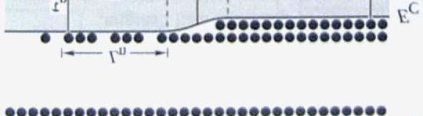
14 Inversion eso domains formation ato in GaN M. Stutzmann et al. phys. stat. sol. (b) 228, 505 (2001) Domain formation due to nucleation of Ga-face and N-face grains Need well-defined nucleation step


15 Al 2 O 3 surface termination and polarity Epi-ready sapphire is O-terminated O-removal during High-T thermal treatment M. Stutzmann t et al., phys. stat. t sol. (b) 228,, 505 (2001)
16 PL in In-containing alloys Spatially varying energy of excited state due to atomic-scale inhomogeneity Stokes shift between absorption and emission


17 Polarization of strained and unstrained nitrides O. Ambacher et al., J. Appl. Phys. 85,, 3222 (1999)
18 Polarization and band profiles Left image: Polar (0001) oriented heterostructure Right image: non-polar a-face orientation S. Chichibu, nature materials 5, 810 (2006)


19 GaN columns on AlN/Si(111) Potential for columnar LEDs with much higher light extraction ti efficiency i
20 Sensitivity of the human eye Green: night vision Gray: day vision


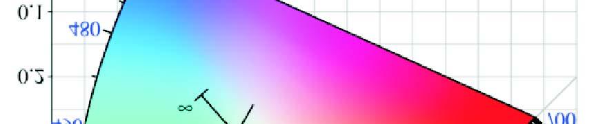

21 CIE chromaticity diagram CIE = Commission Internationale de l Eclairage


22 Blue-pumped YAG phosphor R Pump wavelength 460 nm LER decreases with blue leakage! M.R. Krames, J. Display Technol. 3,, 160 (2007)
23 Chromaticity for blue-pumped YAG y CCT ~ 5000 K for 35 % blue leakage (LER = 328 lm/w) Theoretical maximum LES ~ 283 lm/w at CRI ~ 80 M.R. Krames, J. Display Technol. 3,, 160 (2007)
24 Maximum down-conversion efficiency CE=(P leak +P conv )/P )/P LED M.R. Krames et al., J. Display Technol. 3, 160 (2007)
25 Near band edge PL of alloys S. Chichibu, nature materials 5, 810 (2006)
26 Quantum efficiencies of HBLEDs J.M. Phillips, Laser & Photon Review 1, No. 4, 2007
27 Maximum LER for RYGB (CCT = 3000 K) All linewidths 1 nm CCT = 3000 K JM J.M.. Phillips et al., Laser & Photon Rev. 1, 307 (2007)
28 Scheme of GaN-HEMT
29 Sheet charge density at AlGaN/GaN interfaces O. Ambacher et al., J. Appl. Phys. 85, 3222 (1999)
30 Al Al 0.09 Ga Ga 0.91 N/GaN heterostructure Sheet electron density Mobility cm 2 /Vs at 4 K cm -2 at 4 K 12 cm C.R. Elsass et al., Jap. J. Appl. Phys. 39, L1023 (2000)
31 Comparison of HEMTs F. Schwierz, TU Ilmenau 2003
32 Comparison of transport properties p Typical room temperature data for important interfaces
33 Band structures of Si, Ge and α-sn Empirical pseudopotential method, Chelikowski and Cohen 1976
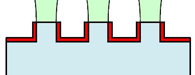
34
35 Band structures of tetrahedrally bonded d semiconductors Note the close similarity of the Ge band structure with that of GaAs around Γ
36 Ge under biaxial ba a strain M.V. Fischetti & S.E. Laux, J. Appl. Phys. 80, 2234 (1996)
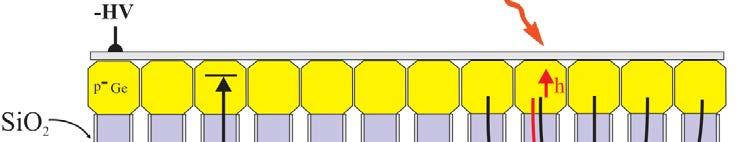
37 Improved hole transport: compressive strain unstrained E compressively strained E k k LH SO HH Strain lifts HH-LH degeneracy Heavy holes become lighter Anti-crossing with LH band leads to non-parabolicity
38 Modulation doped strained Ge quantum wells Typical structure used for high mobility hole transport t
39 Record hole mobility of Ge quantum well B. Rössner et al., APL 84,, 3058 (2004) Most recently (University of Warwick 2012) > cm 2 /Vs!


40 Ge photodiodes for IR detection Band gap shift by thermally induced tensile strain in Ge on Si
41 Bandgap shift through thermal annealing Extraction of the direct band-gap energy for the as grown ( ) and annealed ( ) 1 µm thick absorption layer G. Isella et al., Semicond. Sci. Technol. 22,, S26 (2007)


42 CMOS-integrated pixel detector CMOS circuit 2.5 µm, 1 metal, 1 poly process of CNM Barcelona R. Kaufmann et al., JAP 110, (2011)
43 IR image sensor with integrated Ge photodetectors R. Kaufmann et al., JAP 110, (2011)
44 Absorbed photons vs. X-reay tube voltage

45 Current-voltage measurements Au wire A p-si p-ge Ge Ge Ge n-si


46 In-situ measurements in SEM-chamber SEM chamber SEM picture of top contact on individual germanium tower tungsten tip A p-si p-ge I d Ge Ge Ge V d 2 µm Conductive tungsten tip n-si I-V characteristics measured in-situ SEM Zeiss Nvision µm

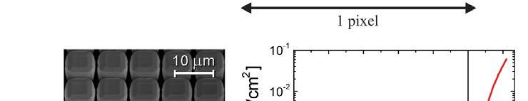

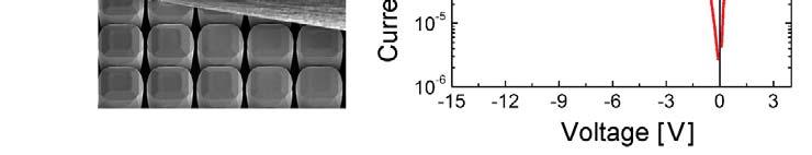
47 Definition of detector pixels H. von Känel, Europhysics News 43,, 18 (2012)
Semiconductor Nanostructures
 I H. von Känel Laboratorium für Festkörperphysik ETHZ Moore s Law Doubling of transistor density in less than every 2 years International Roadmap for Semiconductors Evolution of LED performance Haitz law
3.46 OPTICAL AND OPTOELECTRONIC MATERIALS
 Badgap Engineering: Precise Control of Emission Wavelength Wavelength Division Multiplexing Fiber Transmission Window Optical Amplification Spectrum Design and Fabrication of emitters and detectors Composition
Gallium Nitride Based HEMT Devices
 Gallium Nitride Based HEMT Devices Keyan Zang SMA5111/6.772 Compound Semiconductor Materials and Devices May 14 th, 2003 Courtesy of Keyan Zang. Used with permission. Outline Introduction Device Structure
Crystalline Silicon Solar Cells
 12 Crystalline Silicon Solar Cells As we already discussed in Chapter 6, most semiconductor materials have a crystalline lattice structure. As a starting point for our discussion on crystalline silicon
InGaN quantum dot based LED for white light emitting
 Emerging Photonics 2014 InGaN quantum dot based LED for white light emitting Luo Yi, Wang Lai, Hao Zhibiao, Han Yanjun, and Li Hongtao Tsinghua National Laboratory for Information Science and Technology,
Grundlagen der LED Technik
 www.osram-os.com Grundlagen der LED Technik Dr. Berthold Hahn 8.3.14 Ilmenau 1 Dateienname ORG CODE Initiale Titel/Veranstaltung TT/MM/JJJJ Grundlagen der LED Technik 1. Einführung 2. Lichterzeugung im
Materials: Structures and Synthesis
 微纳光电子材料与器件工艺原理 Materials: Structures and Synthesis Xing Sheng 盛兴 Department of Electronic Engineering Tsinghua University xingsheng@tsinghua.edu.cn 1 Optical and Electronic Devices LEDs lasers waveguides
Introduction to Nitride Semiconductor Blue Lasers and Light Emitting Diodes
 Introduction to Nitride Semiconductor Blue Lasers and Light Emitting Diodes Edited by Shuji Nakamura and Shigefusa F. Chichibu London and New York Contents 1. Basics Physics and Materials Technology of
ECCI of AlGaN/GaN HEMT structures grown on Si
 ECCI of AlGaN/GaN HEMT structures grown on Si D. Thomson 1, G. Naresh-Kumar 1, B. Hourahine 1, C. Trager-Cowan 1, P. Wright 2 and T. Martin 2 1 Dept. Of Physics, SUPA, University of Strathclyde, Glasgow
LIGHT EMITTING. A Brief Introduction
 LIGHT EMITTING DIODES A Brief Introduction By Vishnu Kumar Deki Electronics Contents: Introduction of LEDs Comparison with FTL Comparison with CFL Lighting Basics Costing and ROI LED Basics LED Chip Specifications
Materials Characterization
 Materials Characterization C. R. Abernathy, B. Gila, K. Jones Cathodoluminescence (CL) system FEI Nova NanoSEM (FEG source) with: EDAX Apollo silicon drift detector (TE cooled) Gatan MonoCL3+ FEI SEM arrived
Structural and optical properties of AlInN and AlGaInN on GaN grown by metalorganic vapor phase epitaxy
 Journal of Crystal Growth 195 (1998) 309 313 Structural and optical properties of AlInN and AlGaInN on GaN grown by metalorganic vapor phase epitaxy Shigeo Yamaguchi*, Michihiko Kariya, Shugo Nitta, Hisaki
Molecular Beam Epitaxy Growth of GaAs 1-x Bi x
 Molecular Beam Epitaxy Growth of GaAs 1-x Bi x Dan Beaton, Ryan Lewis, Xianfeng Lu, Mostafa Masnadi-Shirazi, Sebastien Tixier, Erin Young, Martin Adamcyk, UBC, Vancouver, BC B. Fluegel, A. Mascarenhas,
Semiconductor Optoelectronics Prof. M.R. Shenoy Department of Physics Indian Institute of Technology, Delhi
 Semiconductor Optoelectronics Prof. M.R. Shenoy Department of Physics Indian Institute of Technology, Delhi Lecture - 32 Light Emitting Diode-V Materials and Applications (Refer Slide Time: 00:47) Today
Supporting Information for. Design of Dipole-Allowed Direct Band Gaps in Ge/Sn. Core-Shell Nanowires
 Supporting Information for Design of Dipole-Allowed Direct Band Gaps in Ge/Sn Core-Shell Nanowires Elisabeth Pratidhina, Sunghyun Kim, and K. J. Chang* Department of Physics, Korea Advanced Institute of
An advantage of thin-film silicon solar cells is that they can be deposited on glass substrates and flexible substrates.
 ET3034TUx - 5.2.1 - Thin film silicon PV technology 1 Last week we have discussed the dominant PV technology in the current market, the PV technology based on c-si wafers. Now we will discuss a different
Optoelectronic characterization of Au/Ni/n-AlGaN photodiodes after annealing at different temperatures
 Optoelectronic characterization of Au/Ni/n-AlGaN photodiodes after annealing at different temperatures PNM Ngoepe *, WE Meyer, M Diale, FD Auret, L van Schalkwyk Department of Physics, University of Pretoria,
High Transmittance Ti doped ITO Transparent Conducting Layer Applying to UV-LED. Y. H. Lin and C. Y. Liu
 High Transmittance Ti doped ITO Transparent Conducting Layer Applying to UV-LED Y. H. Lin and C. Y. Liu Department of Chemical Engineering and Materials Engineering, National Central University, Jhongli,
Lecture 10: Semiconductors
 Lecture 10: Semiconductors Definitions Band structure, band gap Basic principles Doping Electrical properties Important semiconductor materials Main group semiconductors Transition metal main group SCs
Crystal Structure. Insulin crystals. quartz. Gallium crystals. Atoms are arranged in a periodic pattern in a crystal.
 Crystal Structure Atoms are arranged in a periodic pattern in a crystal. The atomic arrangement affects the macroscopic properties of a material. Many important materials (silicon, steel) are crystals
Improved color rendering and luminous efficacy in phosphor-converted white light-emitting diodes by use of dual-blue emitting active regions
 Improved color rendering and luminous efficacy in phosphor-converted white light-emitting diodes by use of dual-blue emitting active regions Roya Mirhosseini 1, Martin F. Schubert 1, Sameer Chhajed 1,
Hetero-epitaxy of III-V Compounds by MOCVD on Silicon Substrates
 1.119/1.33795 The Electrochemical Society Hetero-epitaxy of III-V Compounds by MOCVD on Silicon Substrates Chak Wah TANG, Zhenyu ZHONG, and Kei May LAU Department of Electronic and Computer Engineering
ON THE PHOTOMAGNETIC EFFECT IN CdTe THIN FILMS EVAPORATED ONTO UNHEATED SUBSTRATES
 Journal of Optoelectronics and Advanced Materials Vol. 7, No. 2, April 2005, p. 811-815 ON THE PHOTOMAGNETIC EFFECT IN CdTe THIN FILMS EVAPORATED ONTO UNHEATED SUBSTRATES G. G. Rusu *, M. Rusu, M. Caraman
Characteristics of Heat-Annealed Silicon Homojunction Infrared Photodetector Fabricated by Plasma-Assisted Technique
 PHOTONIC SENSORS / Vol. 6, No. 4, 216: 345 35 Characteristics of Heat-Annealed Silicon Homojunction Infrared Photodetector Fabricated by Plasma-Assisted Technique Oday A. HAMMADI * Department of Physics,
AlGaN/GaN based HEMT Device for High Power Applications
 AlGaN/GaN based HEMT Device for High Power Applications 1 Kajal Jain, 2 Shivani Saxena 1 M.tech VLSI, Banasthali Vidyapith 2 Assistant Professor, Department of Electronics, Banasthali Vidyapith, Banasthali,
Supporting Information. AlN/h-BN Heterostructures for Mg Dopant-Free Deep Ultraviolet Photonics
 Supporting Information AlN/h-BN Heterostructures for Mg Dopant-Free Deep Ultraviolet Photonics D. A. Laleyan 1,2, S. Zhao 1, S. Y. Woo 3, H. N. Tran 1, H. B. Le 1, T. Szkopek 1, H. Guo 4, G. A. Botton
Comparison Study of Structural and Optical Properties of In x Ga 1-x N/GaN Quantum Wells with Different In Compositions
 Comparison Study of Structural and Optical Properties of In x Ga 1-x N/GaN Quantum Wells with Different In Compositions Yong-Hwan Kwon, G. H. Gainer, S. Bidnyk, Y. H. Cho, J. J. Song, M. Hansen 1, and
AlGaN/GaN HFETs on 100 mm Silicon Substrates for Commercial Wireless Applications
 Materials Technology Using Si as a substrate material for GaN based devices enables a variety of applications and manufacturing technologies. The 100 mm Si substrate platform allows use of larger state-of-the-art
9/4/2008 GMU, ECE 680 Physical VLSI Design
 ECE680: Physical VLSI Design Chapter II CMOS Manufacturing Process 1 Dual-Well Trench-Isolated CMOS Process gate-oxide TiSi 2 AlCu Tungsten SiO 2 p-well poly n-well SiO 2 n+ p-epi p+ p+ 2 Schematic Layout
Transmission Mode Photocathodes Covering the Spectral Range
 Transmission Mode Photocathodes Covering the Spectral Range 6/19/2002 New Developments in Photodetection 3 rd Beaune Conference June 17-21, 2002 Arlynn Smith, Keith Passmore, Roger Sillmon, Rudy Benz ITT
Germanium and silicon photonics
 76 Technical focus: III-Vs on silicon optoelectronics Germanium and silicon photonics Mike Cooke reports on recent research using germanium to enable infrared light-emitting devices to be created on silicon
EFFECTS OF Si, Al 2 O 3 AND SiC SUBSTRATES ON THE CHARACTERISTICS OF DBRS STRUCTURE FOR GaN BASED LASER
 Journal of Physical Science, Vol. 17(2), 151 159, 2006 151 EFFECTS OF Si, Al 2 O 3 AD SiC SUSTRATES O THE CHARACTERISTICS OF DRS STRUCTURE FOR Ga ASED LASER.M. Ahmed*, M.R. Hashim and Z. Hassan School
Fraunhofer IZM Berlin
 Fraunhofer IZM Berlin Advanced Packaging for High Power LEDs Dr. Rafael Jordan SIIT Agenda Gluing Soldering Sintering Transient Liquid Phase Bonding/Soldering Thermo Compression Junction Temperature Measurements
Improve the performance of MOCVD grown GaN-on-Si HEMT structure
 Improve the performance of MOCVD grown GaN-on-Si HEMT structure Dr. Xiaoqing Xu Stanford Nanofabrication Facility Abstract The SNF installed a new metalorganic chemical vapor deposition (MOCVD) system
SEMICONDUCTORS R. A. SMITH CAMBRIDGE AT THE UNIVERSITY PRESS. M.A., PH.D. Head of the Physics Department Royal Radar Establishment Malvern J 959
 SEMICONDUCTORS BY R. A. SMITH M.A., PH.D. Head of the Physics Department Royal Radar Establishment Malvern CAMBRIDGE AT THE UNIVERSITY PRESS J 959 CONTENTS Chapter 1. The Elementary Properties of Semiconductors
Effect of Process Parameters on the Growth of N-polar GaN on Sapphire by MOCVD
 Effect of Process Parameters on the Growth of N-polar GaN on Sapphire by MOCVD A Thesis Submitted For the Degree of Doctor of Philosophy in the Faculty of Science by G R Krishna Yaddanapudi Department
Lecture 14: Semiconductors
 Lecture 14: Semiconductors Definitions Band structure, band gap Basic principles Doping Electrical properties Important semiconductor materials Main group semiconductors Metal oxide semiconductors Applications
MOCVD technology in research, development and mass production. H. Juergensen. AIXTRON AG, Kackertstr , D Aachen, Germany
 MOCVD technology in research, development and mass production H. Juergensen AIXTRON AG, Kackertstr. 15-17, D-52072 Aachen, Germany e-mail: info@aixtron.com, phone: +49-241-8909-0, fax: +49-241-8909-40
LANDOLT-BORNSTEIN. Zahlenwerte und Funktionen aus Naturwissenschaften und Technik. Neue Serie. Gesamtherausgabe: K.-H. Hellwege
 LANDOLT-BORNSTEIN Zahlenwerte und Funktionen aus Naturwissenschaften und Technik Neue Serie Gesamtherausgabe: K.-H. Hellwege Gruppe III: Kristall- und Festkörperphysik Band 17 Halbleiter Herausgeber: O.
In-Situ Characterization During MOVPE Growth of III-Nitrides using Reflectrometry
 18 Annual Report 1999, Dept. of Optoelectronics, University of Ulm In-Situ Characterization During MOVPE Growth of III-Nitrides using Reflectrometry Christoph Kirchner and Matthias Seyboth The suitability
Semiconductor Physics
 10p PhD Course Semiconductor Physics 18 Lectures Nov-Dec 2011 and Jan Feb 2012 Literature Semiconductor Physics K. Seeger The Physics of Semiconductors Grundmann Basic Semiconductors Physics - Hamaguchi
High Performance AlGaN Heterostructure Field-Effect Transistors
 Kyma Inc. Contract ABR DTD 1/8/07; Prime: FA8650-06-C-5413 1 High Performance AlGaN Heterostructure Field-Effect Transistors Program Objectives The primary objectives of this program were to develop materials
Impurity free vacancy disordering of InGaAs quantum dots
 JOURNAL OF APPLIED PHYSICS VOLUME 96, NUMBER 12 15 DECEMBER 2004 Impurity free vacancy disordering of InGaAs quantum dots P. Lever, H. H. Tan, and C. Jagadish Department of Electronic Materials Engineering,
Bulk crystal growth. A reduction in Lg will increase g m and f oper but with some costs
 Bulk crystal growth The progress of solid state device technology has depended not only on the development of device concepts but also on the improvement of materials. A reduction in Lg will increase g
ET3034TUx High efficiency concepts of c- Si wafer based solar cells
 ET3034TUx - 4.4 - High efficiency concepts of c- Si wafer based solar cells In the previous block we have discussed various technological aspects on crystalline silicon wafer based PV technology. In this
The components of. Technology focus: III-Vs on silicon. Fiber-optic gallium antimonide
 76 Direct growth of III-V laser structures on silicon substrates From infrared to ultraviolet wavelengths, researchers are enabling lower-cost production of silicon photonics. Mike Cooke reports. The components
Final Report for AOARD Grant FA Development of direct band gap group-iv. March, 2012
 Final Report for AOARD Grant FA2386-11-1-4037 Development of direct band gap group-iv semiconductor with the incorporation of Sn March, 2012 Name of Principal Investigators: Prof. H. H. Cheng - e-mail
Detrimental effects of dislocations II
 Detrimental effects of dislocations II Band diagram around a charged dislocation e - - - - - - - - Charged dislocation line Electrons get scattered by charged dislocations Mobility vs. sheet charge in
GROWTH AND INVESTIGATION OF INDIUM ARSENIDE BASED DIODE HETEROSTRUCTURES FOR MID INFRARED APPLICATION
 GROWTH AND INVESTIGATION OF INDIUM ARSENIDE BASED DIODE HETEROSTRUCTURES FOR MID INFRARED APPLICATION V.A. Gevorkyan, K.M. Gambaryan, and M.S. Kazaryan Yerevan State University, E-mail: vgev@ysu.am 1.
PROPERTIES OF ADVANCED SEMICONDUCTOR MATERIALS
 PROPERTIES OF ADVANCED SEMICONDUCTOR MATERIALS GaN, AIN, InN, BN, SiC, SiGe Edited by Michael E. Levinshtein The Ioffe Institute, Russian Academy of Sciences Sergey L. Rumyantsev The Ioffe Institute, Russian
Electrochemical Oxidation, Threading Dislocations and the Reliability of GaN HEMTs
 Electrochemical Oxidation, Threading Dislocations and the Reliability of GaN HEMTs Carl V. Thompson 1,3 Dept. of Materials Science and Engineering, M.I.T. Primary collaborators: Wardhana A. Sasangka 1,
Silicon-on-insulator (SOI) was developed in the
 was developed in the") 66 Silicon-on-insulator substrates for compound semiconductor applications Mike Cooke reports on research developments reaching towards high-power electronics and infrared optical communications. Silicon-on-insulator
66 Silicon-on-insulator substrates for compound semiconductor applications Mike Cooke reports on research developments reaching towards high-power electronics and infrared optical communications. Silicon-on-insulator
GSMBE growth of GaInAsP/InP 1.3 mm-tm-lasers for monolithic integration with optical waveguide isolator
 Journal of Crystal Growth 278 (25) 79 713 www.elsevier.com/locate/jcrysgro GSMBE growth of GaInAsP/InP 1.3 mm-tm-lasers for monolithic integration with optical waveguide isolator F. Lelarge a,, B. Dagens
Direct growth of III-V quantum dot materials on silicon
 Direct growth of III-V quantum dot materials on silicon John Bowers, Alan Liu, Art Gossard Director, Institute for Energy Efficiency University of California, Santa Barbara http://optoelectronics.ece.ucsb.edu/
GROWTH AND CHARACTERIZATION OF GeSn AND SiGeSn ALLOYS FOR OPTICAL INTERCONNECTS
 GROWTH AND CHARACTERIZATION OF GeSn AND SiGeSn ALLOYS FOR OPTICAL INTERCONNECTS A DISSERTATION SUBMITTED TO THE DEPARTMENT OF MATERIALS SCIENCE AND ENGINEERING AND THE COMMITTEE ON GRADUATE STUDIES OF
INGAN BASED LIGHT EMITTING DIODE AND LASER DIODE THE PRESENT AND THE FUTURE
 52 INGAN BASED LIGHT EMITTING DIODE AND LASER DIODE THE PRESENT AND THE FUTURE Nasser N.Morgan a,b and Ye Zhizhen a a State key Laboratory of Silicon materials, Zhejiang University, Hangzhou, China b Faculty
Development and Applications of Wide Bandgap Semiconductors
 1 Development and Applications of Wide Bandgap Semiconductors 1.1 Optical Devices (A. Yoshikawa) 1.1.1 Wide Bandgap Semiconductors Indispensable for Short Wavelength Optical Devices As the name implies,
Wafer bowing control by polarity management of MOCVD AlN growth
 Wafer bowing control by polarity management of MOCVD AlN growth Ritsumeikan University Misaichi Takeuchi Collaboration with Prof. Aoyagi, Ritsumeikan University LayTec seminar, Oct. 18 2009, Jeju, Korea
CHAPTER 4 LED LIGHT EMITTING DIODE
 CHAPTER 4 LED LIGHT EMITTING DIODE 1 PART II LIGHT EMITTING DIODE LED are semiconductor p-n junctions that under forward bias conditions can emit What is LED? radiation by electroluminescence in the UV,
Red InGaP light-emitting diodes epitaxially grown on engineered Ge-on-Si substrates
 Red InGaP light-emitting diodes epitaxially grown on engineered Ge-on-Si substrates The MIT Faculty has made this article openly available. Please share how this access benefits you. Your story matters.
Optical pumping and final metal investigation
 Optical pumping and final metal investigation FLOORS Optical pumping of unstressed device Optical pumping of stressed device Stressing points Trap analysis t=0, As Built t>0, Degradation Final Metal Study
ECE440 Nanoelectronics. Lecture 08 Review of Solid State Physics
 ECE440 Nanoelectronics Lecture 08 Review of Solid State Physics A Brief review of Solid State Physics Crystal lattice, reciprocal lattice, symmetry Crystal directions and planes Energy bands, bandgap Direct
THE PAST, PRESENT, AND FUTURE OF LIGHTING
 THE PAST, PRESENT, AND FUTURE OF LIGHTING WHY CARE ABOUT LIGHTING? Lighting Statistics 38% of industrial and commercial electricity use is for lighting. 10% to 20% of home electricity use is for lighting.
Improving performance of InGaN LEDs on sapphire substrates
 80 Improving performance of InGaN LEDs on sapphire substrates Mike Cooke reports on research into semipolar growth, quantum well barrier composition and zinc oxide enhancements. Commercial indium gallium
Introduction to Energy Efficient Lighting ECEN 2060
 Introduction to Energy Efficient Lighting ECEN 2060 US Residential & Commercial Energy Consumption 1 Energy losses during generation, transmission and distribution of electricity * DOE, EIA, Annual Energy
ISSN: ISO 9001:2008 Certified International Journal of Engineering and Innovative Technology (IJEIT) Volume 3, Issue 6, December 2013
 Volume 3, Issue 6, December 2013") ISSN: 2277-3754 Fabrication and Characterization of Flip-Chip Power Light Emitting Diode with Backside Reflector Ping-Yu Kuei, Wen-Yu Kuo, Liann-Be Chang, Tung-Wuu Huang, Ming-Jer Jeng, Chun-Te Wu, Sung-Cheng
ISSN: 2277-3754 Fabrication and Characterization of Flip-Chip Power Light Emitting Diode with Backside Reflector Ping-Yu Kuei, Wen-Yu Kuo, Liann-Be Chang, Tung-Wuu Huang, Ming-Jer Jeng, Chun-Te Wu, Sung-Cheng
Nanomaterials and Analytics Semiconductor Nanocrystals and Carbon Nanotubes. - Introduction and Preparation - Characterisation - Applications
 Nanomaterials and Analytics Semiconductor Nanocrystals and Carbon Nanotubes - Introduction and Preparation - Characterisation - Applications Simple molecules
The effect of rapid thermal annealing to device performance of InGaAs/AlGaAs quantum well laser diodes
 Indian Journal of Pure & Applied Physics Vol. 55, May 2017, pp. 333-338 The effect of rapid thermal annealing to device performance of InGaAs/AlGaAs quantum well laser diodes P L Gareso a*, M Buda b, H
INVESTIGATION OF PHOTOVOLTAIC PROPERTIES of p-inse/n-cds HETEROJUNCTION SOLAR CELLS
 Journal of Ovonic Research Vol. 1, No. 3, May - June 214, p. 67-73 INVESTIGATION OF PHOTOVOLTAIC PROPERTIES of p-inse/n-cds HETEROJUNCTION SOLAR CELLS K. YILMAZ * Pamukkale University, Science and Arts
Published in: Proceedings of the 19th Annual Symposium of the IEEE Photonics Benelux Chapter, 3-4 November 2014, Enschede, The Netherlands
 Characterization of Ge/Ag ohmic contacts for InP based nanophotonic devices Shen, L.; Wullems, C.W.H.A.; Veldhoven, van, P.J.; Dolores Calzadilla, V.M.; Heiss, D.; van der Tol, J.J.G.M.; Smit, M.K.; Ambrosius,
Topological crystalline insulators. Tomasz Story Institute of Physics, Polish Academy of Sciences, Warsaw
 Topological crystalline insulators Tomasz Story Institute of Physics, Polish Academy of Sciences, Warsaw Topological crystalline insulators - outline 1. Introduction topological crystalline insulators
The next thin-film PV technology we will discuss today is based on CIGS.
 ET3034TUx - 5.3 - CIGS PV Technology The next thin-film PV technology we will discuss today is based on CIGS. CIGS stands for copper indium gallium selenide sulfide. The typical CIGS alloys are heterogeneous
The Blue Laser Diode. Shuji Nakamura Stephen Pear ton Gerhard Fasol. The Complete Story. Springer
 Shuji Nakamura Stephen Pear ton Gerhard Fasol The Blue Laser Diode The Complete Story Second Updated and Extended Edition With 256 Figures and 61 Tables Springer Contents 1. Introduction 1 1.1 LEDs and
Strained SiC:Ge Layers in 4H SiC formed by Ge Implantation. M.W. Dashiell, G. Xuan, Xin Zhang, E. Ansorge and J. Kolodzey
 Mat. Res. Soc. Symp. Proc. Vol. 742 2003 Materials Research Society K6.7.1 Strained SiC:Ge Layers in 4H SiC formed by Ge Implantation M.W. Dashiell, G. Xuan, Xin Zhang, E. Ansorge and J. Kolodzey Department
This is the author s final accepted version.
 Law, T.K., Lim, F., Li, Y., Yeong, K.K. G., Sng, G.K. E., Uvarajan, M.V., and Teo, J.W. R. (2016) Implications of phosphor coating on the thermal characteristics of phosphor-converted white LEDs. IEEE
High reflectivity and thermal-stability Cr-based Reflectors and. n-type Ohmic Contact for GaN-based flip-chip light-emitting.
 High reflectivity and thermal-stability Cr-based Reflectors and n-type Ohmic Contact for GaN-based flip-chip light-emitting diodes Kuang-Po Hsueh, a * Kuo-Chun Chiang, a Charles J. Wang, b and Yue-Ming
Characterization and Fabrication of 90nm Strained Silicon PMOS using TCAD
 Characterization and Fabrication of 90nm Strained Silicon PMOS using TCAD M. A. Abd Hamid and F. Sulaiman, Member, IEEE Abstract The paper focuses on the enhancement of conventional 90nm PMOS using graded
Thermally-Enhanced Generation of Solar Fuels
 Thermally-Enhanced Generation of Solar Fuels Xiaofei Ye, Liming Zhang, Madhur Boloor, Nick Melosh, William Chueh Materials Science & Engineering, Precourt Institute for Energy Stanford University Fundamentals
Cubic GaN Light Emitting Diode Grown by Metalorganic Vapor-Phase Epitaxy
 TANAKA IEICE TRANS. and NAKADAIRA: ELECTRON., VOL. CUBIC E83-C, GaN LIGHT NO. 4 APRIL EMITTING 2000 DIODE 585 PAPER Special Issue on Blue Laser Diodes and Related Devices/Technologies Cubic GaN Light Emitting
Chapter 18: Electrical Properties
 Chapter 18: Electrical Properties What are the physical phenomena that distinguish conductors, semiconductors, and insulators? For metals, how is conductivity affected by imperfections, T, and deformation?
Studies on Si-doped AlGaN Epilayers
 Studies on Si-doped AlGaN Epilayers 47 Studies on Si-doped AlGaN Epilayers Kamran Forghani Growth optimization of Si doped AlGaN epilayers with 20%, 30% and 45%Al content grown on AlGaN-sapphire by MOVPE
Temperature dependence of molecular beam epitaxy of GaN on SiC (0001)
") Temperature dependence of molecular beam epitaxy of GaN on SiC (0001) V. Ramachandran a, A. R. Smith a, R. M. Feenstra a and D. W. Greve b a Department of Physics, b Department of Electrical and Computer
Temperature dependence of molecular beam epitaxy of GaN on SiC (0001) V. Ramachandran a, A. R. Smith a, R. M. Feenstra a and D. W. Greve b a Department of Physics, b Department of Electrical and Computer
RSC Advances.
 This is an Accepted Manuscript, which has been through the Royal Society of Chemistry peer review process and has been accepted for publication. Accepted Manuscripts are published online shortly after
EPITAXY extended single-crystal film formation on top of a crystalline substrate. Homoepitaxy (Si on Si) Heteroepitaxy (AlAs on GaAs)
 Heteroepitaxy (AlAs on GaAs)") extended single-crystal film formation on top of a crystalline substrate Homoepitaxy (Si on Si) Heteroepitaxy (AlAs on GaAs) optoelectronic devices (GaInN) high-frequency wireless communication devices
extended single-crystal film formation on top of a crystalline substrate Homoepitaxy (Si on Si) Heteroepitaxy (AlAs on GaAs) optoelectronic devices (GaInN) high-frequency wireless communication devices
2014 NOBEL LECTURE IN PHYSICS
 Background Story of the Invention of Efficient Blue InGaN Light Emitting Diodes SHUJI NAKAMURA SOLID STATE LIGHTING AND ENERGY ELECTRONICS CENTER MATERIALS AND ECE DEPARTMENTS UNIVERSITY OF CALIFORNIA,
Ge Incorporation in SiC and the Effects on Device Performance
 Ge Incorporation in SiC and the Effects on Device Performance K. J. Roe, M. W. Dashiell, G. Xuan*, E. Ansorge, G. Katulka, N. Sustersic, X. Zhang and J. Kolodzey Department of Electrical and Computer Engineering
Nanostructured Solar Cells: From Academic Research to Commercial Devices
 Nanostructured Solar Cells: From Academic Research to Commercial Devices V. Mitin 1,2, A. Sergeev 1,2, N. Vagidov 1,2, K. A. Sablon 3, J. W. Little 3 and K. Reinhardt 4 1 OPEN, OptoElectronic Nanodevices
SOLID-STATE lighting (SSL) based on LEDs is an emerging
 based on LEDs is an emerging") 1028 IEEE JOURNAL OF SELECTED TOPICS IN QUANTUM ELECTRONICS, VOL. 15, NO. 4, JULY/AUGUST 2009 LEDs for Solid-State Lighting: Performance Challenges and Recent Advances Mary H. Crawford, Member, IEEE (Invited
1028 IEEE JOURNAL OF SELECTED TOPICS IN QUANTUM ELECTRONICS, VOL. 15, NO. 4, JULY/AUGUST 2009 LEDs for Solid-State Lighting: Performance Challenges and Recent Advances Mary H. Crawford, Member, IEEE (Invited
Applications for HFETs
 Applications for HFETs Ga-face Quantum well is formed at the interface AlGaN GaN Buffer P SP P SP P PE -σ s +σ int 2DEG + ve φ b d σ comp AlGaN σ int E 0 GaN E c E F c-plane sapphire σ 2DEG σ surf Higher
Physics and Material Science of Semiconductor Nanostructures
 Physics and Material Science of Semiconductor Nanostructures PHYS 570P Prof. Oana Malis Email: omalis@purdue.edu Lecture 6 Bulk semiconductor growth Single crystal techniques Nanostructure fabrication
Quarterly Report EPRI Agreement W
 Quarterly Report EPRI Agreement W08069-07 PI: S.J. Pearton, University of Florida (Co-investigators F. Ren, C.R. Abernathy, R.K. Singh, P.H. Holloway, T.J. Anderson, M. Berding, A. Sher, S. Krishnimurthy,
Ivan Bazarov Physics Department, Cornell University. Fundamental processes in III-V photocathodes; application for high-brightness photoinjectors
 Ivan Bazarov Physics Department, Cornell University Fundamental processes in III-V photocathodes; application for high-brightness photoinjectors 07/21/09 I.V. Bazarov, III-V Photocathodes, ERL09 2 Contents
Simple fabrication of highly ordered AAO nanotubes
 Journal of Optoelectronic and Biomedical Materials Volume 1, Issue 1, March 2009, p. 79-84 Simple fabrication of highly ordered AAO nanotubes N. Taşaltin a, S. Öztürk a, H. Yüzer b, Z. Z. Öztürk a,b* a
Control of Dislocations and Stress in AlGaN on Sapphire Using a Low Temperature Interlayer
 H. Amano et al.: Dislocations and Stress in AlGaN on Sapphire 683 phys. stat. sol. (b) 216, 683 (1999) Subject classification: 68.55.Jk; S7.14; S7.15 Control of Dislocations and Stress in AlGaN on Sapphire
1. Photonic crystal band-edge lasers
 TIGP Nanoscience A Part 1: Photonic Crystals 1. Photonic crystal band-edge lasers 2. Photonic crystal defect lasers 3. Electrically-pumped photonic crystal lasers 1. Photonic crystal band-edge lasers Min-Hsiung
Crystalline Silicon Solar Cells With Two Different Metals. Toshiyuki Sameshima*, Kazuya Kogure, and Masahiko Hasumi
 Crystalline Silicon Solar Cells With Two Different Metals Toshiyuki Sameshima*, Kazuya Kogure, and Masahiko Hasumi Tokyo University of Agriculture and Technology, 2-24-16 Naka-cho, Koganei, Tokyo 184-8588,
Microelectronics Devices
 Microelectronics Devices Yao-Joe Yang 1 Outline Basic semiconductor physics Semiconductor devices Resistors Capacitors P-N diodes BJT/MOSFET 2 Type of Solid Materials Solid materials may be classified
THIN AlN FILMS GROWTH ON Si (III) BY HYDRIDE VAPOR PHASE EPITAXY
 BY HYDRIDE VAPOR PHASE EPITAXY") THIN AlN FILMS GROWTH ON Si (III) BY HYDRIDE VAPOR PHASE EPITAXY S. Raevschi, V. Davydov 1, Y. Zhilyaev 1, L. Gorceac, and V. Botnariuc Department of Physics, Moldova State University, 60, A. Mateevich
THIN AlN FILMS GROWTH ON Si (III) BY HYDRIDE VAPOR PHASE EPITAXY S. Raevschi, V. Davydov 1, Y. Zhilyaev 1, L. Gorceac, and V. Botnariuc Department of Physics, Moldova State University, 60, A. Mateevich
OPTICAL MODE PATTERN STUDY OF GAN BASED LEDS WITH AND WITHOUT NANOSCALE TOP GRATING
 OPTICAL MODE PATTERN STUDY OF GAN BASED LEDS WITH AND WITHOUT NANOSCALE TOP GRATING by Greg Chavoor Senior Project ELECTRICAL ENGINEERING DEPARTMENT California Polytechnic State University San Luis Obispo
Growth and characterization of tensile strained Ge on Ge 1-x Sn x buffers for novel channel layers
 The 5th International Symposium on Advanced Science and Technology of Silicon Materials (JSPS Si Symposium), Nov. 10-14, 2008, Kona, Hawaii, USA Growth and characterization of tensile strained Ge on Ge