Pulse-Electroplating: Process Parameters and Their Influence on the Formed Microstructure
|
|
|
- Amber Ray
- 6 years ago
- Views:
Transcription
1 Pulse-Electroplating: Process Parameters and Their Influence on the Formed Microstructure Diploma work in the Master Programme Materials Engineering DANIEL MELCIU NAVIN MAIDEE Diploma work No. 161/2015 Department of Materials and Manufacturing Technology CHALMERS UNIVERSITY OF TECHNOLOGY Gothenburg, Sweden 2015
2 Pulse-Electroplating: Process Parameters and Their Influence on the Formed Microstructure by Daniel Melciu Navin Maidee Diploma work No. 161/2015 at Department of Materials and Manufacturing Technology CHALMERS UNIVERSITY OF TECHNOLOGY Gothenburg, Sweden Diploma work in the Master Programme Materials Engineering Performed at: Department of Materials and Manufacturing Technology Chalmers University of Technology SE Gothenburg Examiner & Supervisor: Professor Uta Klement Department of Materials and Manufacturing Technology Chalmers University of Technology SE Gothenburg
3 Pulse-Electroplating: Process Parameters and Their Influence on the Formed Microstructure Daniel Melciu Navin Maidee Daniel Melciu, 2015 Navin Maidee, 2015 Diploma work No. xx/2015 Department of Materials and Manufacturing Technology Chalmers University of Technology SE Gothenburg Sweden Telephone + 46 (0) CHALMERS Reproservice Gothenburg, Sweden, 2015
4 Pulse-Electroplating: Process Parameters and Their Influence on the Formed Microstructure Daniel Melciu Navin Maidee Department of Materials and Manufacturing Technology Chalmers University of Technology Abstract Nickel-layers with a thickness of a few tens of microns were produced by pulseelectrodeposition using two electrolytic baths (I and II). The influence of temperature and current density on the obtained microstructure was investigated using Electrolyte I while for the effect of Nickel Sulfamate concentration and current density was analyzed using Electrolyte II. In addition, Polyamide fibers included in Hybrix TM sandwich material were coated by pulseelectrodeposition and afterwards investigated. Electrodeposited Nickel was examined in the asprepared state by XRD and SEM. With the help of EBSD technique, orientation maps, pole figures and inverse pole figures were obtained for all samples. Different microstructures were obtained by changing temperature and current density. As a result, the average grain size of asdeposited Nickel varied from 30 nm to 200 nm, depending on plating conditions. Moreover, a <100>-texture is obtained independently of plating conditions. In contrast, when the effect of Nickel Sulfamate concentration and current density was investigated, no preferred orientation, i.e. a weak <110>-texture is attained independently on Nickel Sulfamate concentration and current density. The average grain size of the produced microstructures was in the range of 40 to 50 nm. Concerning the electrodeposition on Polyamide fibers, a Nickel coating was successfully deposited on the fibers. Keywords: Nickel electrodeposition, pulse-electrodeposition, texture, microstructure, nanocrystalline structure, EBSD
5 Table of Contents 1 Introduction Electrodeposition Electrodeposited Nanocrystalline Structure Texture in Nickel Electrodeposition Microstructure in Nickel Electrodeposition Epitaxial Region Influence of Electroplating Parameters on Grain Size Materials and Experimental Procedure Pulse-Electroplating Equipment Substrate Material Stainless Steel Polyamide Fibers Experimental Procedure The Study of Current Density and Temperature Effect on Obtained Microstructure The Study of Nickel Concentration and Current Density Effect on the Obtained Microstructure Experimental Techniques X-Ray Diffraction Scanning Electron Microscopy Electron Backscatter Diffraction Results Surface Characterization Effect of Temperature and Current Density on As-Deposited Nickel Films Effect of Nickel Sulfamate Concentration and Current Density on As-Deposited Nickel Films X-Ray Diffraction Effect of Current Density and Temperature Effect of Nickel Sulfamate Concentration and Current Density Microstructure Analysis Inverse Pole Figures SEM Images EBSD Orientation Maps Grain Size Determination Pulse-Electroplating on Sandwich Material... 31
6 4 Discussion Effect of Current Density and Temperature Effect of Nickel Sulfamate Concentration and Current Density Pulse-Electroplating on Sandwich Material Conclusion Future Recommendations Reference Appendix: Grain Size Determination Appendix: SEM and EBSD Images... Error! Bookmark not defined.
7 Preface The purpose of the present work is to investigate the influence of the process parameters involved in the pulse-electroplating process with regard to the formed microstructure. The project was proposed by Prof. Uta Klement and the entire work was performed at the Department of Materials and Manufacturing Technology at Chalmers University of Technology, Gothenburg, Sweden. The electroplating was performed using two electrolytic solutions named Electrolyte I and Electrolyte II, respectively. Electrolyte I was already in place and its chemical composition was only partially known while Electrolyte II was mixed and developed during this thesis work. We would like to take this opportunity to express our gratitude to all the people who have been helpful during the project. Firstly, our gratitude is addressed to Prof. Uta Klement who provided us with this very exciting project. We thank her for the given time and support. Especially, we are grateful for the help in the investigation techniques and the fact that she has been encouraging us during the project. Secondly, we would like to thank the following persons who have helped us during the project by introducing us to equipment or by giving us assistance or advice: Yiming Yao for the introduction to SEM, Gold-sputtering and Electropolishing equipment. Eric Tam for XRD training and help in interpreting the results. Also, for supervising the mixing of Electrolyte II. Roger Sagdahl for discussions regarding the functionality of the electroplating equipment.

8 1 Introduction 1.1 Electrodeposition For more than two centuries, electrodeposition has been a successful technique for coating substrate surfaces with different metallic materials. Various types of substrate materials can be used in electrodeposition including pure metals, conductive polymeric materials, metal composites and alloys. During the electrodeposition process, the deposition of metal ions on the substrate surface at the cathode is caused by charge transfer between cathode and anode in the electrolyte. The charge transfer in this case is driven by an external electrical circuit (figure 1) [1]. Previously, electrodeposition technique was widely used for providing new surface properties to the substrate such as corrosion-, wear- and erosion resistance and in some cases it was used for decorating purposes. However, due to the advancement in materials engineering, nowadays, electrodeposition can be applied to more specific applications such as tailoring magnetic surfaces and electronic components [2]. Figure 1: The schematic movement of ions in the electroplating process. The microstructure of the plated layers is dependent on the various parameters of the electrolyte bath such as bath composition, ph value, temperature, current density, additives, etc. In addition, grain size, texture and internal stress of the substrate can also influence the formation of the electrodeposit [3]. The outstanding performance of the electroplating process like its high production rate with low investment cost makes the process more effective and favorable in the production scale. The porosity-free microstructure is the distinct feature that can be obtained by this technique in the form of thin film coating or free-standing parts [3][4][5][6]. Furthermore, the grain size obtained by performing pulse-electrodeposition 1
9 can be below 10 nm. As a result, several properties can be influenced by this change of grain size into nanoscale. 1.2 Electrodeposited Nanocrystalline Structure Nanostructured material was first introduced by Gleiter [7] as the structure that is formed in non-equilibrium state. When the grains are getting smaller than 100 nm, hardness and wear resistance are increasing due to the large amount of grain boundaries and triple junctions comprising the intercrystalline region. The increase in hardness and yield strength in nanomaterials is in accordance with the Hall-Petch relationship. This behavior is valid down to about 10 nm (depending on material) where an apparent softening occurs which is described by the inverse Hall-Petch relationship. At these small grain sizes, other deformation mechanisms set in [2][4][8]. However, there are also some properties that show no or only a slight dependence on grain size such as Young s modulus, thermal expansion, heat capacity and saturation magnetization [2][8]. Different techniques can be utilized to synthesis nanostructure materials such as sol gel technique, spark erosion, gas condensation, ball-milling and electroplating technique. In the case of electroplating, the nanostructure of as-deposited materials can be obtained by using pulse current instead of direct current [6]. Pulse-electroplating is one of the most attractive techniques due to the distinctive structures obtained by the electrochemical process and the outstanding properties of the nanostructure. The various parameters that influence the nanostructures produced by electroplating technique are now more in the research objective for better understanding in the way how each parameter is involved in the formation mechanism of the nanocrystalline structure [8]. Crystallization of materials occurs with the competition between the nucleation of new grains and the growth of the existing grains. The dominance of either nucleation or growth process is dependent on the processing conditions. In electrodeposition, the nucleation rate can be increased in the condition of high current density (overpotential) and low surface diffusion of ad-atoms of existing grains which results in the achievement of nanostructure. On the other hand, grain growth can occur in the condition of low current density (overpotential) and high surface diffusion [2][3]. Generally, the microstructure produced by electrodeposition is influenced by the bath conditions. However, in the very first layer of the deposited film, epitaxial grains can be found which are influenced by the crystallographic structure of the substrate rather than the bath conditions. This layer is formed for only a few microns. When the film layer becomes thicker, the grains will grow in a preferred orientation depending on the bath conditions [9][10]. 1.3 Texture in Nickel Electrodeposition According to Amblard et al. [10], two important theories have been used to describe the anisotropy of the texture of Nickel electrodeposit which are explained from the opposite viewpoints. One theory says that the competition in nucleation is responsible for the anisotropy while the theory one suggests that it is the competitive growth that determines the anisotropy. However, the literature data have shown that both theories are insufficient to fully describe all experimental results. 2
10 Pangarov [9] suggested that the anisotropy of the texture of Nickel electrodeposit is dependent on the nucleation process which is related to the overpotential. As mentioned by Pangarov, the possible textures of the metals with fcc structure when increasing overpotential are <111>-<100>-<110>-<311>-<210> [9]. However, this theory can be explained only in the pure condition which means that neither the influence of defects on the substrate surface nor the adsorption of other species in the electrolyte is considered. However, in reality, metallic surfaces are usually not defect-free. Additionally, for the transition materials with high surface energy such as Nickel, it is less likely that it does not contain any adsorbed species. This means, the conditions are then considered to be unrealistic [10]. Opposite to Pangarov s theory, other authors state that the anisotropic texture of the Nickel electrodeposit is determined by the growth process. In this way, the hydrogen adsorption (Hads) becomes an important factor for controlling the texture during electrodeposition. When the level of Hads increases, the texture develops from <110> to <100> and finally <200>. Although this theory includes the consideration of the Hads influence on the film texture, it is insufficient to explain all the possible preferred orientations of the Nickel electrodeposit. This is due to the fact that Hads is not the only species in the electrolyte that could inhibit the growth of the Nickel crystals [10][11]. In an additive-free bath, the <110>-texture is the inhibition growth mode influenced by Hads while the <211>-texture is the result of the presence of Ni(OH)2. Also, <210>-texture is affected by Hydrogen gas in the electrolyte. The growth of the <100>-texture cannot be related to any inhibiting species and this is why this texture is considered as the free growth mode. Each type of species can be linked to the ph value of the electrolyte. Hence, the presence of a texture at a specific ph value and current density can be predicted as in the diagram presented by Amblard et al. [10]. In pulse-electrodeposition, the adsorption and desorption of inhibitors on the substrate surface can be hindered by the Ton- (plating time) and Toff-time (relaxation time) which provide the possibility of creating deposit with better properties [12]. Molecular inhibitors will desorb from the substrate surface during the relaxation period (Toff) while Hads and anions behave contrarily, i.e. they will adsorb to the interface and inhibit the growth of the Nickel coating on the surface. The perturbation that is dependent on the frequency and duty cycle of the electroplating system plays an important role in determining the characteristics of the Nickel electrodeposit. A small perturbation level provides less structural defects with larger grain size, while at high perturbation, <110> growth mode is dominant for all kinds of inhibiting species. This is due to the inhibition of Hads which becomes the only factor governing the growth of the Nickel electrodeposit [12]. 1.4 Microstructure in Nickel Electrodeposition Epitaxial Region The epitaxial layer is a very fine-grained layer formed next to the substrate surface with the same structure and grain orientation as the substrate material. The main advantage of this layer is to reduce the interfacial energy between the substrate and the electrodeposited layer. The difference in lattice constants between substrate and deposited materials results in the occurrence of a misfit strain in the epitaxial layer. This leads to a high dislocation density in order to accommodate the misfit strain. A tolerable strain supported by the 3
11 microstructure can be up to 12%. Experimental results of the previous literature showed that the thickness of the epitaxial layer of electrodeposited Nickel on a Cu substrate can reach up to 100 nm before the columnar grains with no orientation relationship to the substrate are formed [13] Influence of Electroplating Parameters on Grain Size The various parameters involved in the Nickel electrodeposition have been studied for revealing the relation with the microstructure in order to improve the process of synthesizing nanostructured Nickel [6][14][15][16][17][18]. Although the nanostructured Nickel have already been produced, the tailoring of Nickel electrodeposit properties is still complex. This is due to the uncertain results when the effects of all plating parameters are involved. Compared with the direct current (DC) electroplating [19][20], the on-time and off-time intervals in pulse-electroplating have a significant influence on the microstructure of the Nickel electrodeposit. The longer on-time and higher current density is applied, the smaller grain size down to a few nanometers can be produced. The higher number of duty cycle initiate more nucleation sites for Nickel crystals on the substrate and leads to the smaller grain size. According to Ravi et al. [20], the grain size linearly decreases with the higher number of duty cycle. For the influence of current density on the grain size, the results are still controversial in different studies. According to Rashidi [21], in pulse-electroplating process, the grain size can be decreased with an increase in current density but the effect is just substantial up to 7.5 A/dm 2. After that, a further increase in the current density will not influence the grain refinement to the same extent. This finding is in contrast to some experiments [14][15][18] on DC electroplating of Nickel where the grain size linearly increases with increasing the current density. The effect of temperature on the grain morphology is still not generally identified. However, it is accepted that the deposition rate, coating quality and some other properties can be altered with only small variations in bath temperature [22]. From the results proposed by Rashidi [21], the grain size of electrodeposits will increase when the bath temperature increases. But this behavior is only valid for temperatures above 55 C. This observation is also in accordance with the diagram introduced by Dini [23] and the study on nanocrystalline electrodeposits by Natter et al. [24]. Additionally, the grain size of the electrodeposited materials is also dependent on other parameters such as the frequency and the concentration of bath additives like saccharin which acts as a grain refiner. 4
 Characterization of the electrodeposited materials. (3) Deposition of a Nickel coating on polymer fibers in a sandwich structure and investigation of the coating quality. 2.")
12 2 Materials and Experimental Procedure The experimental section of the current thesis work had three objectives: (1) Production of materials with nanocrystalline microstructure by adjusting the process parameters. (2) Characterization of the electrodeposited materials. (3) Deposition of a Nickel coating on polymer fibers in a sandwich structure and investigation of the coating quality. 2.1 Pulse-Electroplating Equipment All samples were produced in the pulse-electroplating equipment illustrated in figure 2. The equipment contains the following parts: 1. Propeller 2. Plating bath of 2 liters 3. Heating device for warming the electrolyte to the required temperature 4. Pulse generator 5. Oscilloscope for reading the current parameters a 5


13 b c Figure 2: Pulse-Electroplating equipment: a) Overview of the equipment, b) anode and cathode, i.e. sample holder and basket with Nickel pellets, and c) set-up of cathode, anode and propeller. 2.2 Substrate Material Stainless Steel As substrate material, a stainless steel plate of 30 mm * 60 mm * 1.5 mm was used. The stainless steel had the advantage that the Nickel coating could be easily stripped off afterwards. No mechanical preparation of the substrate was required before the electrodeposition process. However, a cleaning and degreasing operation was performed. The substrate was rinsed both under tap water and by ethanol and afterwards blow-dried in order to avoid stains. After the electrodeposition process, the coated layers were removed from the sample holder and cleaned. This means, the electrodeposited films were rinsed under distilled water and subsequently by ethanol. To avoid stains, the coated samples were cleaned for 5 or 10 minutes in an ultrasonic bath containing ethanol and afterwards blow-dried Polyamide Fibers A set of experiments was performed in order to investigate if a Nickel electrodeposit could be applied to strengthen the Hybrix sandwich material produced by Lamera AB. The material investigated consisted of stainless steel plates between which Polyamide 6.6 fibers were attached with help of an Epoxy adhesive. The cross section of the sandwich material can be seen in figure 3. Since the Polyamide fibers are not conductive, Gold sputtering was chosen to create a conductive layer on the fibers. The process was performed using an Edwards Sputter Coater S150B where the process was carried out at 1 kv within five minutes. 6
 and a newly mixed electrolyte (Electrolyte II).")
14 Figure 3: Cross section of the composite material showing the bottom steel plate and the attached fibers. The top steel plate is missing to facilitate Gold-sputtering. 2.3 Experimental Procedure The intended experiments were performed by using two different electrolytic baths, an existing electrolyte (Electrolyte I) and a newly mixed electrolyte (Electrolyte II). The chemical composition of each electrolyte will be described later-on in this section The Study of Current Density and Temperature Effect on Obtained Microstructure In this study, Electrolyte I was used to produce the samples for studying the effect of current density and temperature on Nickel electrodeposit. The electrolyte contains Nickel Sulfamate as the main ingredient and has a ph value in the range of 3 to 5 (see Appendix). The solution is additive-free and contains Boric acid, Magnesium Chloride and Natrium Citrate. A set of experiments was performed at different current densities, i.e. 2, 10 and 20 A/dm 2. In addition to the current density, also temperature was varied between 35 C and 75 C with a step size of 10 degrees. This resulted in 15 samples where five different temperatures were used at each of the three current density value as shown in table 1. 7
15 Table 1: List of the conditions used for studying the current density and temperature effect on Nickel electrodeposit. Current Density (A/dm2) Temperature ( C) The Study of Nickel Concentration and Current Density Effect on the Obtained Microstructure Electrolyte II was used to produce the samples for studying the effect of Nickel Sulfamate concentration and current density on the formed microstructure. The electrolyte contains a substantial amount of Nickel Sulfamate (Ni(SO3N2).4H2O) as the main source of Nickel ions. In addition, Boric acid (H3BO3) and Magnesium Chloride were added. The solution was continuously developed to investigate the influence of the Nickel Sulfamate concentration on the appearance and microstructure of the electrodeposits. The initial chemical composition of the electrolyte is stated in table 2 and the development of the electrolyte is shown in table 3. Also, the conditions used for producing the samples are displayed in table 4. Table 2: The initial chemical composition of Electrolyte II showing the concentration of Nickel Sulfamate in Molar [M]. Chemical Component Nickel Sulfamate Ni(NH₂SO₃)₂ [M] Boric Acid H₃BO₃ [g] Magnesium Chloride MgCl₂ [g] Sodium Citrate C 6H 5Na 3O 7 [g] Water H₂O [L] Amount
16 Table 3: The development of Nickel Sulfamate concentration in Electrolyte II. Chemical Component Nickel Sulfamate Ni(NH₂SO₃)₂ [M] 1st Concentration 2nd Concentration 3rd Concentration 4th Concentration 5th Concentration 6th Concentration Table 4: List of the conditions used for studying the Nickel Sulfamate concentration and current density effect on the formed microstructure. Nickel Sulfamate Concentration (Molar) Current Density (A/dm 2 ) Experimental Techniques For investigation of the microstructure changes (i.e. grain size, texture, grain size distribution, and surface topography) that take place when changing the process parameters, different advanced characterization techniques were used X-Ray Diffraction X-ray diffraction (XRD) is used to determine the interplanar spacing of crystalline materials which provide information about the phase composition, residual stresses and atomic structure. It also gives an impression about the overall texture when the diffractogram is compared to that of a powder standard (which has a random texture and is found in the database). The working principle is based on a monochromatic X-ray beam which irradiates the sample (under various angles ϴ) while the XRD detector is rotating and measures the intensity of the diffracted beam as a function of 2ϴ (ϴ is the diffracted angle). The information is collected, plotted and then compared to the data found in the database. [25]. 9
17 Investigations were performed by a Bruker D8 Advance X-ray diffractometer using a Cranode (wavelength = Å) and a generator power of 35 kw and 40 ma. The angle ϴ was varied in the range of 65⁰ to 140⁰. All samples were scanned at room temperature for about 6 minutes each. No sample preparation was required apart from that the samples were cut to a length of 40 mm in order to fit into the sample holder Scanning Electron Microscopy In Scanning Electron Microscopy (SEM), an electron beam scans the sample surface and as a result, various signals can be obtained such as backscattered electrons, secondary electrons, and characteristic X-rays, which can be used for imaging and chemical analysis Electron Backscatter Diffraction Electron Backscatter Diffraction (EBSD) is a technique that provides microstructural and crystallographic information, e.g. local texture, grain morphology, grain boundary distribution, grain size and grain size distribution [26]. The technique is able to inspect a considerable amount of grains in a relatively short period of time. The EBSD detector is an attachment to the SEM. With the cooperation of the required evaluation software, it can be used to measure and identify electron backscattered diffraction patterns (EBSP or Kikuchi patterns). To obtain so-called orientation map, a color-coded representation of the grains in the microstructure, the sample is tilted 70 towards the EBSD detector in the SEM and a defined area is scanned with a suitable step size (depending by the grain size). At each point (pixel), an EBSP is captured with a CCD (Charge Coupled Device) camera and the software indexes the obtained pattern by comparing it with the crystallographic data of the expected phase which has to be selected before the investigation. A specific color is addressed to the pixel which represents the measured orientation. In case that indexing was not possible as a result of undefined phase, overlapping patterns from adjacent grains or due to poor pattern quality, the pixel will be referred to as zero solution. In this thesis work, the samples were investigated using a Leo 1550 Gemini FEG-SEM equipped with a Nordlys II EBSD detector and Channel 5 software by HKL Technologies. Afterwards, the obtained data was analyzed further by Channel 5 software with respect to grain size distribution in order to obtain pole figures and inverse pole figure diagrams. Prior to EBSD analysis, the samples were prepared by electropolishing. A Struers LectroPol-5 device with a Struers A2 electrolyte consisting of 70% Perchloric acid and 30% 2-Butoxyethanol was used for 10 seconds at a voltage of 31 V. The size of the electropolished samples was around 1 cm. After electropolishing, the samples were rinsed with Ethanol and placed in water for ending the corrosion process before they were blowdried. 10
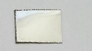
18 3 Results 3.1 Surface Characterization Effect of Temperature and Current Density on As-Deposited Nickel Films Based on the experiments, all the produced samples show a bright or semi-bright surface where the degree of brightness differs in each sample depending on the plating condition. In the temperature range between 55 C to 75 C, the as-plated Nickel films tend to have duller surface when the current densities decrease. However, when produced at 35 C, the films are shinier when the current density is decreased. In the case of a bath temperature of 45 C, the sample with the best appearance was produced at 10 A/dm 2. In general, at all current densities, the Nickel coatings tend to become duller when the bath temperature is decreased except for the sample produced at 35 C with 2 A/dm 2 current density that shows a really bright-shiny surface. Waviness on the surface can be found in the samples produced at low plating temperature. However, the waviness disappears when the current density is decreased (figure 5). Pitting is another defect that can be observed in this study (figure 6). It is usually found at moderate plating temperatures and its size is smaller when the current density decreases. The thickness of the film obviously varies with the current density. When using the same deposition time, the film thickness increases with the increase in current density. The appearance of the produced samples is summarized in table 5 and 6. Table 5: The effect of current density and temperature on the apperance of Nickel electrodeposits. C urrent Density Temperature B 2 A/dm D 10 A/dm 2 - W D 20 A/dm 2 - W 35 C 45 C 55 C 65 C 75 C Description : 1st line > [Bright = B, Dull = D] 2nd line >[ Pitting = P] 3rd line >[wavy = W] B - - B P - D P W B - - B P - B P - B - - B - - B - - B - - B - - B


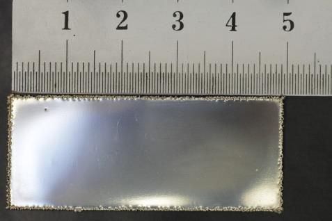
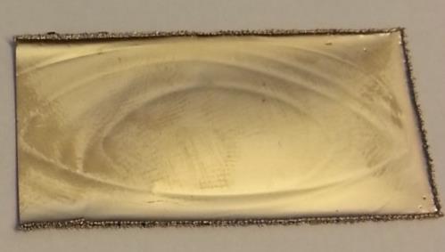
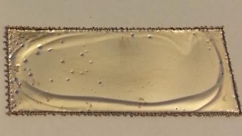
19 Table 6: The surface appearance of Nickel electrodeposits produced by varying current density and temperature. Temperature Current Density 35 C 45 C 55 C 65 C 75 C 2 A/dm 2 10 A/dm 2 20 A/dm 2 Figure 4: Bright and smooth surface of the sample produced at 20 A/dm 2 and 65 C. Figure 5: Waviness of the sample produced at 20 A/dm2 and 35 C. Figure 6: Pitting observed in the sample produced at 20 A/dm 2 and 45 C. 12


20 3.1.2 Effect of Nickel Sulfamate Concentration and Current Density on As-Deposited Nickel Films The appearance of the samples produced with Electrolyte II is very different from those produced with Electrolyte I (figure 7). The distinct appearance of these films is the very thin dark layer on the surface that can be observed in all samples. The degree of the brightness varies with the Nickel Sulfamate concentration and also the current density. With the increase in Nickel Sulfamate concentration, the brightness of the films gradually increases. It can also be noticed that the films gets brighter when the current density increases. It is observed that the dark thin layer on the film surface is very sensitive to grease and oil. When touching the samples with bare hands, stains easily show up and they are hard to remove. It is also noticed that this layer has a sensitive surface, i.e. that it can easily be scratched even by a plastic tool. The appearances of the samples produced in this study are summarized in table 7. Table 7:The surface apperance of Nickel electrodeposits produced by varying current density and Nickel Sulfamate concentration. Current Density Nickel Sulfamate Concentration 2 A/dm2 10 A/dm2 20 A/dm M 2.15 M 2.44 M 2.89 M 13

21 Figure 7: Comparison of the appearance of the samples produced under the same plating condition with Electrolyte I (Top) and Electrolyte II (Bottom). 3.2 X-Ray Diffraction Effect of Current Density and Temperature In table 8, the results of XRD measurements for the current densities of 2 A/dm 2, 10 A/dm 2 and 20 A/dm 2 are shown. The information contained in the table consists of the intensity values observed for {111}- and {200}-reflections. Additionally, texture coefficient and the grain size as obtained by Scherrer equation are also shown in the table. The Scherrer equation is shown in the formula below. τ = Kλ βcosθ τ = the average grain size K = shape factor λ = X-ray wavelength β = half the maximum intensity (FWHM) θ = the Bragg angle The intensity of both {111}- and {200}-reflections increase when the current density increases. The variation in peak intensity values and texture coefficient of the samples produced with different conditions can be seen in table 8. However, XRD patterns of all samples are the same in all conditions. Representative diffractograms of the samples from this experiment are shown in figure 8 and 9. 14
22 Table 8: Summary of XRD data of the analyzed Nickel electrodeposits showing the intensity in {111} and {200} plane, texture coefficient, and grain size calcualated by using Scherrer equation. Current Density Temperature {111} Reflection Intensity {200} Reflection Intensity Texture Coefficient ( I {200}/ I {111} ) 2θ FWHM Grain Size by Scherrer Equation (nm) 2 A/dm2 35 C ,76 81,10 0,818 19,00 45 C ,60 81,00 0,666 23,31 55 C ,81 81,05 0,612 25,38 65 C ,08 81,10 0,753 20,64 75 C ,21 81,10 0,756 20,55 10 A/dm2 35 C ,94 81,01 0,682 22,77 45 C ,62 81,00 0,904 17,18 55 C ,46 81,00 0,817 19,01 65 C ,59 81,10 0,675 23,02 75 C ,33 81,10 0,696 22,33 20 A/dm2 35 C ,48 81,11 0,409 38,00 45 C ,00 81,00 0,586 26,50 55 C ,24 81,11 0,865 17,96 65 C ,56 81,00 0,733 21,18 75 C ,89 81,00 0,749 20,73 {200} {111} Figure 8: XRD pattern of an electrodeposit produced at 2 A/dm 2 and 35 C. 15
23 Intensity Intensity {200} {111} Diffraction angle (2ϴ) Figure 9: XRD pattern of an electrodeposit produced at 20 A/dm 2 and 35 C. A representative XRD pattern of the samples was plotted in comparison with the XRD pattern of Nickel powder (figure 10 and 11). The XRD patterns of Nickel electrodeposits show a very strong intensity in {200} reflection, while the {220} reflection is not present on the XRD profiles. The difference in XRD patterns between Nickel electrodeposits and Nickel powder indicates that Nickel electrodeposits have a certain texture (Nickel powder is considered to have a random texture) {111} {200} {220} Diffraction angle Figure 10: XRD pattern of Nickel powder. 16
24 Intensity {200} {111} {220} Figure 11: Comparison of XRD patterns of as-deposited Nickel and Nickel powder Effect of Nickel Sulfamate Concentration and Current Density Table 9 provides the XRD data collected from electrodeposits produced with Electrolyte II. In addition to intensity values observed for {111} and {200} reflections, also data for the {220} reflection are included. Additionally, texture coefficient and the grain size obtained by Scherrer equation are provided in table 9. The schematic plots of two different XRD patterns of the samples produced in this study are exhibited in figure 12 and 13. The samples produced at 2 A/dm 2 show a higher value of {111} peak intensity while the samples produced at 20 A/dm 2 reveal a higher {220} peak {111} {200} {220} Diffraction angle (2ϴ) Figure 12: XRD profile of the sample produced at 2 A/dm 2 and 2.44 M of Nickel Sulfamate concentration showing the highest intensity in the {111} peak. 17
25 Intensity {220} {111} {200} Diffraction angle (2ϴ) Figure 13: XRD profile of the sample produced at 20 A/dm 2 and 2.44 M of Nickel Sulfamate concentration showing the highest intensity in the {220} peak. Table 9: XRD data collected from the samples produced by varying current density and Nickel Sulfamate concentration. Nickel Sulfamate Concentration Current Density {111} Reflection Intensity {200} Reflection Intensity {220} Reflection Intensity Texture Coefficient (I (200)/I (111)) 2θ FWHM Grain Size by Scherrer Equation (nm) 1.85 M 2 A/dm A/dm ,30 68,40 0,624 22,88 20 A/dm ,26 68,50 0,567 25, M 2 A/dm ,23 68,40 0,534 26,73 10 A/dm ,24 68,50 0,569 25,10 20 A/dm ,30 133,80 1,254 24, M 2 A/dm ,22 68,50 0,510 28,01 10 A/dm ,25 68,50 0,521 27,42 20 A/dm ,35 133,70 1,140 26, M 2 A/dm ,23 68,41 0,536 26,63 10 A/dm ,35 133,81 1,175 25,62 20 A/dm ,34 133,71 1,125 26,70 18
26 Relative intensity The increase in current density enhances the dominance of {220} reflection in XRD at all Nickel Sulfamate concentrations as can be seen in figure 14. Additionally, with the higher concentration of Nickel Sulfamate in solution, a slight increase in each peak intensity can be observed (table 9). {111} 20 A/dm^2 10 A/dm^2 {220} {200} 2 A/dm^ Diffraction angle (2θ) Figure 14: The effect of current density on {111} and {220} peak in XRD profiles of the samples produced at 2.44 M of Nickel Sulfamate concentration. Both XRD patterns of the samples produced in this study were compared to the XRD pattern of Nickel powder to investigate the existence of the texture in the produced microstructures. The schematic plots of the comparisons can be seen in figures 15 and 16. The difference in XRD patterns between as-deposited Nickel films and Nickel powder demonstrates the development of texture in the microstructures of the samples produced in this study. 19
27 {111} {220} {200} Figure 15: Comparison of XRD patterns of the as deposited Nickel film produced at 2 A/dm 2 and Nickel powder. {111} {220} {220} Figure 16: Comparison of XRD patterns of the as-deposited Nickel film produced at 20 A/dm 2 and Nickel powder. 3.3 Microstructure Analysis Inverse Pole Figures Inverse pole figures were plotted form the data obtained by EBSD. These are used for analyzing the crystallographic orientation in the microstructure of the as-deposited Nickel films. In all cases, the growth direction is parallel to the Z axis. Contouring is applied with the setting of half width at 10 and the data clustering limit is 3. 20

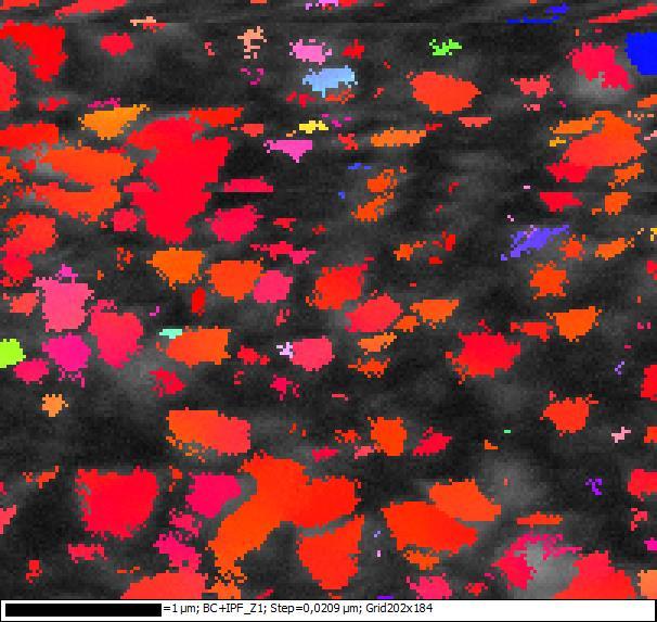
28 Regarding the information of the samples produced with Electrolyte I, texture is not influenced by the change in temperature and current density. All the as-prepared samples show a strong preferred orientation of <100> in the growth direction. A representative inverse pole figure of the samples is shown in figure 17. Figure 17: Inverse pole figure of sample being representative for all samples produced with Electrolyte I. The samples produced with Electrolyte II at 2 A/dm 2 with different Nickel Sulfamate concentrations show a random texture (figure 18). In contrast, as-deposited Nickel films produced at 20 A/dm 2 with different Nickel Sulfamate concentrations show a weak <110>-texture parallel to the growth direction (figure 19). a) b) 21
29 c) Figure 18: Inverse pole figures of the samples produced with Electrolyte II at 2 A/dm 2 with Nickel Sulfamate concentration of a) 2.15M b) 2.44M and c) 2.89M. Figure 19: Inverse pole figure of the sample produced with Electrolyte II at 20 A/dm 2 with Nickel Sulfamate concentration of 2.89 M SEM Images SEM images were obtained by Forward Scattered Diffraction (FSD) detector. The images illustrate the impression of topography of the microstructures. All samples were observed in top view, i.e. in the growth direction of the grains. All samples were investigated at the same magnification at 10k to compare the characteristic of the microstructure at different plating conditions. The samples produced with Electrolyte I at 20 A/dm 2 in bath temperature of 35 C and 45 C reveal the microstructures consisted of big grains with asymmetric shape distributed randomly in a matrix of small grains (figure 20a and 20b). While the samples produced in high bath temperature with different current densities display fine grains well distributed all over the area of investigation. A representative SEM image of fine grain samples is shown in figure

 45 C.")

30 a b Figure 20: SEM images of samples produced with Electrolyte I at 20 A/dm 2 and a bath temperature of a) 35 C and b) 45 C. Figure 21: SEM image of sample produced with Electrolyte I at 20 A/dm 2 and a bath temperature of 55 C. 23
 10 A/dm 2 and 2.")

31 The samples produced with Electrolyte II in all plating conditions reveal very fine grains dispersed evenly in the microstructure. The representative microstructures of the samples are shown in figure 22. a b Figure 22: SEM images of samples produced with Electrolyte II at a) 10 A/dm 2 and 2.15M of Nickel Sulfamate concentration and b) 2 A/dm 2 and 2.44M of Nickel Sulfamate concentration EBSD Orientation Maps The crystallographic orientation of the grains was obtained by the orientation map. The crystallographic direction of grains was colored with respect to the color key of inverse pole figure (figure 23). Noise reduction was applied in the measurement. So-called wild spikes were extrapolated to remove the single spots that are considered as the noise in the results. The extrapolation of zero solutions was performed with 6 neighboring pixels at a critical angle of 10. During measurement of orientation maps, drift occurred which affected the precision of grain morphology analysis. 24


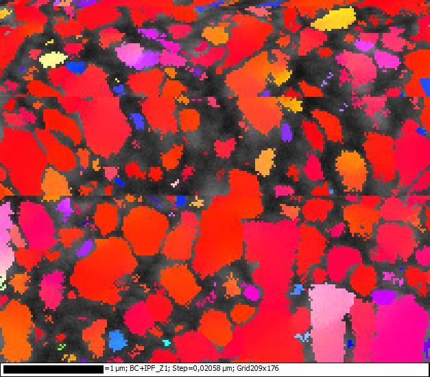
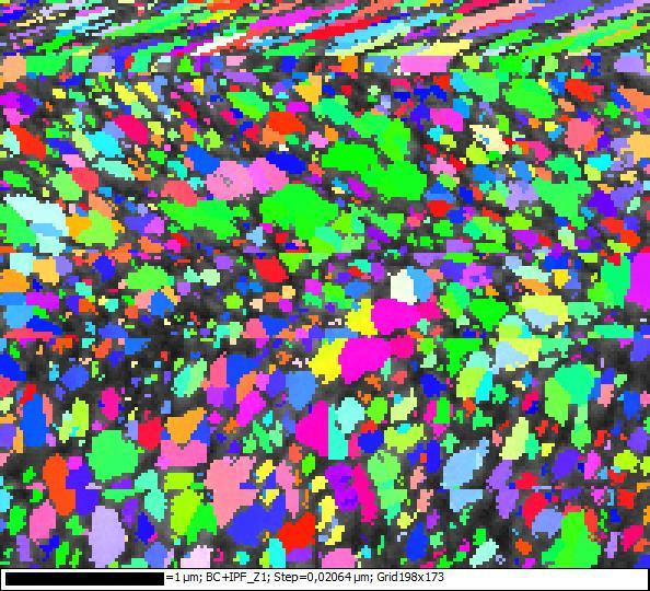
32 Only the orientation maps of the normal direction (Z-axis parallel to the growth direction) are shown. All samples produced with Electrolyte I show a very strong texture in <100> but a different grain morphology. The samples produced at 20 A/dm 2 with bath temperature of 35 C and 45 C, respectively, reveal coarse grain structure (figure 24). The microstructures of samples produced with Electrolyte I at high temperature with all current densities show a combination of fine and coarse grains distributed evenly in the investigated area (figure 25). However, a high fraction of zero solution (which most likely is due to the small grain size) can be observed in these samples (see Appendix). Figure 23: Color key for crystallographic orientations in inverse pole figure. Figure 24: Orientation map of as-deposited Nickel film produced with Electrolyte I at 20 A/dm 2 and 45 C. 25
33 a b 26
 10 A/dm 2 and 65 C and c) 20 A/dm 2 and 55 C.")

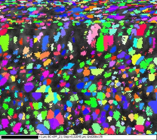
34 c Figure 25: Orientation maps of as-deposited Nickel films produced with Electrolyte I at a) 2 A/dm 2 and 35 C, b) 10 A/dm 2 and 65 C and c) 20 A/dm 2 and 55 C. The samples produced with Electrolyte II show very fine and well distributed grains with the variation in the grain colors. The representative maps of as-deposited Nickel films produced at different conditions are presented in figure 26. a 27
35 b c 28

36 d Figure 26: Orientation maps of as-deposited Nickel films produced with Electrolyte II at a) 2.15M and 2 A/dm 2, b) 2.44M and 2 A/dm 2, c) 2.89M and 2 A/dm 2, and d) 2.89M and 20 A/dm Grain Size Determination Log-normal distribution histograms of the samples were plotted from the detected grains found in the orientation maps. The critical misorientation angle was set to 10. In the present work, the consideration of grain boundary region and zero solution area were excluded. Also the drifting area which affect to the precision of the grain size calculation was excluded. The analysis of the grain size of the samples produced with Electrolyte I at different bath temperatures and current densities is summarized as a bar chart in figure 27 (see Appendix for all data). The average grain sizes of the Nickel electrodeposits produced at 20 A/dm 2 at a bath temperature of 35 C and 45 C are 200±281 nm and 193±219 nm, respectively. The average grain size of 39±66 nm was the lowest average grain size found in the sample produced at 75 C. When prepared at temperature of 55 C and 65 C, Nickel electrodeposits reveal a slightly larger average grain size than the samples produced at 75 C. In contrast to the sample produced at 20 A/dm 2, the samples produced at 2 A/dm 2 and 10 A/dm 2 show an average grain size lower than 100 nm at all plating temperatures. As can be seen from the experimental data, bath temperatures in the range of 55 C to 75 C are providing Nickel electrodeposits to which the grain size is less influenced by 29
37 Grain size (nm) the current density. In contrast, at bath temperatures of 35 C and 45 C, the grain size of as-deposited Nickel films vary considerably with the current density A/dm2 10 A/dm2 2 A/dm Temperature ( C ) Figure 27: Diagram showing the average grain size for samples produced at different bath temperatures and current densities. Nanostructure of Nickel electrodeposits can be observed in all samples produced with Electrolyte II. The average grain size of all investigated samples is displayed in table 10 and 11. From the tables, it can be seen that the current density and the amount of Nickel Sulfamate do not play an important role with respect to the grain size. However, with the increase the current density, an increase in grain size can be observed as shown in table 11, while the tendency of Nickel Sulfamate concentration effect on the average grain size has not been identified (table10). Table 10: Grain size determination of samples produced with Electrotye II at 20 A/dm 2 with different Nickel Sulfamate concentrations. Nickel Sulfamate Concentration Minimum Grain Size (nm) Maximum Grain Size (nm) Number of Investigated Grains Standard Deviation (nm) Average Grain Size (nm) 2.15 M M M
38 Table 11: Grain size determination of samples produced with Electrolyte II at 2.44 M of Nickel Sulfamate concentration with different current densities. Current Density Minimum Grain Size (nm) Maximum Grain Size (nm) Number of Investigated Grains Standard Deviation (nm) Average Grain Size (nm) 2 A/dm A/dm A/dm Pulse-Electroplating on Sandwich Material Due to their outstanding mechanical properties with low weight, sandwich materials are starting to replace the conventional single-structure materials. To further improve their mechanical properties, pulse-electroplating was chosen to strengthen the sandwich material consisting of stainless steel plates to which Polyamide 6.6 fibers were attached. Since the Polyamide fibers are not conductive, Gold sputtering was used to provide a conductive coating on the fibers. As seen when using optical microscopy, the Gold particles were deposited homogeneously on the fiber surface and covered the entire length of the fibers down to the adhesive layer (figure 28a). After two-hour pulse-electroplating, a Nickel electrodeposit could clearly be seen on the fibers situated on the sample edges and in the area around the Copper wires which were attached to improve the conductivity between the fibers and the substrate. Fibers in the middle of the sample and further away from the Copper wires were not covered to the same extent (figure 28b and 28c) even though a Gold layer was present on the fiber surface. 31
 Cross section image showing fibers")
")

39 a 1000µm b c Figure 28: Electrodeposition of Nickel on polymer fibers a) Cross section image showing fibers after Gold sputtering, b) Cross section image showing the electrodeposited Nickel coating on fibers, and c) Image showing the electrodeposited Nickel coating on fibers at the sample edge and close to the attached copper wires. 32
40 4 Discussion 4.1 Effect of Current Density and Temperature The results obtained in the present work show that grain size is influenced by the current density and plating temperature. The grain size increases with the increase in current density. At each plating temperature from 35 C to 65 C, the grain refinement can be observed when the current density decreases. This behavior is consistent with Cziráki et al. [27] where they suggest that the grain size increasing with the increase in current density. This is due to the depletion of Nickel ions on the interface between the deposit layer and electrolyte. The low concentration of the Nickel ions on the cathode surface leads to the low nucleation rate and results in a coarse-grain structure [14]. While, the deposition rate of as-deposited Nickel films on the substrate is still increased with the increase in current density [18]. However, there are some studies [21][28] that reported the effect of current density on a grain refinement differently in the way that the grain size decreases with the increase in current density. This is attributed to the increase of nucleation rate in electrodeposit when the current density increases and as a result, a finegrain structure is obtained. The temperature of the plating bath has two opposite effects on the electrodeposition process. Firstly, the thermodynamic driving force decreases with increasing the bath temperature and results in the increase of critical size of the nuclei. This leads to a low nucleation rate. Secondly, a higher bath temperature enhances the kinetic driving force of the process and results in a higher nucleation rate. In electroplating, the deposition of material is controlled only by the kinetic mechanism since the thermodynamic mechanism can be neglected. The nucleation rate then increases and a fine-grain microstructure can be obtained when the bath temperature is increased [21]. This behavior can be observed in the results of the present work where the grain size of as-deposited Nickel reduces reasonably from 200 nm to 50 nm with increasing the temperature from 35 C to 75 C when using a current density of 20A/dm 2 as plating parameter. The as-deposited Nickel in the present work shows a strong preferred <100>- orientation in the growth direction. This is also reported by Rasmussen et al. [29] where the texture of <100> can be found in a wide range of current densities. Furthermore, when comparing the results of the present work with the texture diagram proposed by Amblard et al. [10], <100> is the dominant texture at a current density above 2 A/dm 2 and at a ph value of 4 which is the same ph value used for the electrolyte in this project. 4.2 Effect of Nickel Sulfamate Concentration and Current Density The grain refinement can be observed with lowering the current density in Nickel electrodeposition. According to literature [27], the high deposition rate causes the depletion of Nickel ions at the deposits-electrolyte interface at high current density which leads to a coarse-grain structure. As can be seen in this experiment, the average grain size of as-deposited Nickel films decreases form 59±69 nm to 48±40 nm when the current density decreases from 20 A/dm 2 to 2 A/dm 2. The samples produced with Electrolyte II show a weak <110>-texture. This indicates that the samples are formed in the growth mode inhibited by Hads [10][11][12]. This is in 33
Characterization of multiple twinned structural units in pulse-electrodeposited nickel
 Characterization of multiple twinned structural units in pulse-electrodeposited nickel U Klement, A Kahrimanidis and Y Yao Materials and Manufacturing Technology, Chalmers University of Technology, Gothenburg,
Observation in the GB (Gentle Beam) Capabilities
 Capabilities") A field-emission cathode in the electron gun of a scanning electron microscope provides narrower probing beams at low as well as high electron energy, resulting in both improved spatial resolution and
A field-emission cathode in the electron gun of a scanning electron microscope provides narrower probing beams at low as well as high electron energy, resulting in both improved spatial resolution and
Development of New Generation Of Coatings with Strength-Ductility Relationship, Wear, Corrosion and Hydrogen Embrittlement Resistance Beyond the
 Development of New Generation Of Coatings with Strength-Ductility Relationship, Wear, Corrosion and Hydrogen Embrittlement Resistance Beyond the Current Materials Accomplishments till date As the structural
Effect of annealing on microstructural development and grain orientation in electrodeposited nickel
 Effect of annealing on microstructural development and grain orientation in electrodeposited nickel by Christos Oikonomou Diploma work No. 51/2011 at Department of Materials and Manufacturing Technology
Carnegie Mellon MRSEC
 Carnegie Mellon MRSEC Texture, Microstructure & Anisotropy, Fall 2009 A.D. Rollett, P. Kalu 1 ELECTRONS SEM-based TEM-based Koseel ECP EBSD SADP Kikuchi Different types of microtexture techniques for obtaining
NEMI Sn Whisker Modeling Group Part 2:Future Work
 NEMI Sn Whisker Modeling Group Part 2:Future Work IPC/NEMI Meeting Maureen Williams, NIST Irina Boguslavsky, NEMI Consultant November 7, 2002 New Orleans, LA Capabilities of NEMI Modeling Group NEMI Fundamental
Growth Of TiO 2 Films By RF Magnetron Sputtering Studies On The Structural And Optical Properties
 Journal of Multidisciplinary Engineering Science and Technology (JMEST) Growth Of TiO 2 Films By RF Magnetron Sputtering Studies On The Structural And Optical Properties Ahmed K. Abbas 1, Mohammed K. Khalaf
Synthesis and Characterization of Cadmium Sulfide Nanoparticles
 Synthesis and Characterization of Cadmium Sulfide Nanoparticles R.Hepzi Pramila Devamani 1*, R.Kiruthika, P.Mahadevi and S.Sagithapriya 2 1 1. Assistant Professor, Department of Physics, V.V.Vanniaperumal
Microstructural Characterization of Materials
 Microstructural Characterization of Materials 2nd Edition DAVID BRANDON AND WAYNE D. KAPLAN Technion, Israel Institute of Technology, Israel John Wiley & Sons, Ltd Contents Preface to the Second Edition
A STUDY ON STRUCTURAL ANALYSIS OF ELECTROPLATED NANO CRYSTALLINE NICKEL BASED THIN FILMS
 ISSN: 0974-1496 e-issn: 0976-0083 CODEN: RJCABP http://www.rasayanjournal.com http://www.rasayanjournal.co.in A STUDY ON STRUCTURAL ANALYSIS OF ELECTROPLATED NANO CRYSTALLINE NICKEL BASED THIN FILMS R.
Fundamentals of X-ray diffraction and scattering
 Fundamentals of X-ray diffraction and scattering Don Savage dsavage@wisc.edu 1231 Engineering Research Building (608) 263-0831 X-ray diffraction and X-ray scattering Involves the elastic scattering of
EBSD Basics EBSD. Marco Cantoni 021/ Centre Interdisciplinaire de Microscopie Electronique CIME. Phosphor Screen. Pole piece.
 EBSD Marco Cantoni 021/693.48.16 Centre Interdisciplinaire de Microscopie Electronique CIME EBSD Basics Quantitative, general microstructural characterization in the SEM Orientation measurements, phase
Investigation on the effect of Electro-co-deposition process parameter bath temperature on Nano Structured Ni-WC Composite coating properties
 International Journal of Materials Science ISSN 0973-4589 Volume 11, Number 1 (2016), pp. 9-15 Research India Publications http://www.ripublication.com Investigation on the effect of Electro-co-deposition
Supplementary Information
 Supplementary Information Disperse fine equiaxed alpha alumina nanoparticles with narrow size distribution synthesised by selective corrosion and coagulation separation Sanxu Pu, Lu Li, Ji Ma, Fuliang
Structural change during cold rolling of electrodeposited copper
 Materials Science Forum Vols. 539-543 (2007) pp. 5013-5018 online at http://www.scientific.net (2007) Trans Tech Publications, Switzerland Structural change during cold rolling of electrodeposited copper
9/28/2013 9:26 PM. Chapter 3. The structure of crystalline solids. Dr. Mohammad Abuhaiba, PE
 Chapter 3 The structure of crystalline solids 1 2 Why study the structure of crystalline solids? Properties of some materials are directly related to their crystal structure. Significant property differences
Supplementary Materials for
 www.sciencemag.org/cgi/content/full/336/6084/1007/dc1 Supplementary Materials for Unidirectional Growth of Microbumps on (111)-Oriented and Nanotwinned Copper Hsiang-Yao Hsiao, Chien-Min Liu, Han-wen Lin,
X-ray diffraction
 2.2.3.- X-ray diffraction 2.2.3.1.- Origins and fundamentals of the technique The first experimental evidence concerning x-ray diffraction was given by Max von Laue who in 1912 demonstrated that x-rays
AP 5301/8301 LABORATORY MANUAL
 AP 5301/8301 LABORATORY MANUAL Department of Physics & Materials Science City University of Hong Kong Contents Table of Contents. 1 Project 1: Scanning Electron Microscopy (SEM). 2 Project 2: Microscopic
TEM and Electron Diffraction Keith Leonard, PhD (1999) U. Cincinnati
 U. Cincinnati") TEM and Electron Diffraction Keith Leonard, PhD (1999) U. Cincinnati Electron Microscopes: Electron microscopes, such as the scanning electron microscope (SEM) and transmission electron microscope (TEM)
TEM and Electron Diffraction Keith Leonard, PhD (1999) U. Cincinnati Electron Microscopes: Electron microscopes, such as the scanning electron microscope (SEM) and transmission electron microscope (TEM)
Imperfections in the Atomic and Ionic Arrangements
 Objectives Introduce the three basic types of imperfections: point defects, line defects (or dislocations), and surface defects. Explore the nature and effects of different types of defects. Outline Point
9/29/2014 8:52 PM. Chapter 3. The structure of crystalline solids. Dr. Mohammad Abuhaiba, PE
 1 Chapter 3 The structure of crystalline solids 2 Home Work Assignments HW 1 2, 7, 12, 17, 22, 29, 34, 39, 44, 48, 53, 58, 63 Due Sunday 12/10/2014 Quiz # 1 will be held on Monday 13/10/2014 at 11:00 am
Synthesis and characterization of pulsed electrodeposited Cu-Y 2 O 3 coating
 Synthesis and characterization of pulsed electrodeposited Cu-Y 2 O 3 coating H. S. Maharana, A. Basu* Department of Metallurgical and Materials Engineering, National Institute of Technology, Rourkela 769008,
9/16/ :30 PM. Chapter 3. The structure of crystalline solids. Mohammad Suliman Abuhaiba, Ph.D., PE
 Chapter 3 The structure of crystalline solids 1 Mohammad Suliman Abuhaiba, Ph.D., PE 2 Home Work Assignments HW 1 2, 7, 12, 17, 22, 29, 34, 39, 44, 48, 53, 58, 63 Due Sunday 17/9/2015 3 Why study the structure
CHAPTER 3. Experimental Results of Magnesium oxide (MgO) Thin Films
 Thin Films") CHAPTER 3 Experimental Results of Magnesium oxide (MgO) Thin Films Chapter: III ---------------------------------------------------------------- Experimental Results of Magnesium oxide (MgO) Thin Films
CHAPTER 3 Experimental Results of Magnesium oxide (MgO) Thin Films Chapter: III ---------------------------------------------------------------- Experimental Results of Magnesium oxide (MgO) Thin Films
EFFECTS OF CURRENT DENSITY ON SIZE AND SURFACE MORPHOLOGY OF HIGH SPEED DIRECT NANO-CRYSTALLINE NICKEL PLATING ON TITANIUM SURFACE
 EFFECTS OF CURRENT DENSITY ON SIZE AND SURFACE MORPHOLOGY OF HIGH SPEED DIRECT NANO-CRYSTALLINE NICKEL PLATING ON TITANIUM SURFACE Noor Zaimah 1, Azieyanti Nurain 1 and Sakhawat Hussain 2 1 Department
INFLUENCE OF PHOSPHOROUS AND UREA ON THE MAGNETIC AND MECHANICAL PROPERTIES OF NANOSTRUCTURED FEPTP FILMS
 , pp. 276-281 INFLUENCE OF PHOSPHOROUS AND UREA ON THE MAGNETIC AND MECHANICAL PROPERTIES OF NANOSTRUCTURED FEPTP FILMS T. M. Selvakumari a*, P. Muthukumar b, S. Ganesan c, and R. N. Emerson d a,b Department
Crystallographic Textures Measurement
 Crystallographic Textures Measurement D. V. Subramanya Sarma Department of Metallurgical and Materials Engineering Indian Institute of Technology Madras E-mail: vsarma@iitm.ac.in Macrotexture through pole
GROWTH AND CHARACTERIZATION OF NANOSTRUCTURED CdS THIN FILMS BY CHEMICAL BATH DEPOSITION TECHNIQUE
 Chalcogenide Letters Vol. 6, No. 8, September 29, p. 415 419 GROWTH AND CHARACTERIZATION OF NANOSTRUCTURED CdS THIN FILMS BY CHEMICAL BATH DEPOSITION TECHNIQUE V. B. SANAP *, B. H. PAWAR, * MSS s College
EFFECT OF DIFFERENT FERROUS CONCENTRATION ON STRUCTURAL AND MECHANICAL PROPERTIES OF ELECTRODEPOSITED FeNiCo THIN FILMS
 EFFECT OF DIFFERENT FERROUS CONCENTRATION ON STRUCTURAL AND MECHANICAL PROPERTIES OF ELECTRODEPOSITED FeNiCo THIN FILMS K. Mohan Rangam Kadiresan 1,V. Senthil Kumar 2 1 Research Scholar, 2 Associate Professor,
In Situ Observation of Dislocation Nucleation and Escape in a Submicron Al Single Crystal
 Supplementary Information for In Situ Observation of Dislocation Nucleation and Escape in a Submicron Al Single Crystal Sang Ho Oh*, Marc Legros, Daniel Kiener and Gerhard Dehm *To whom correspondence
Microstructure Evolution of Polycrystalline Pure Nickel during Static Recrystallization 1
 Materials Transactions, Vol. 43, No. 9 (2002) pp. 2243 to 2248 c 2002 The Japan Institute of Metals Microstructure Evolution of Polycrystalline Pure Nickel during Static Recrystallization 1 Makoto Hasegawa
Studying Effect of Mg Doping on the Structural Properties of Tin Oxide Thin Films Deposited by the Spray Pyrolysis Technique
 Studying Effect of Mg Doping on the Structural Properties of Tin Oxide Thin Films Deposited by the Spray Pyrolysis Technique Abdul Rahman Sakhta 1* Ahmad Khdro Ali Darwisho 3 1.MSc Student, Department
Microstructural characterisation of as-deposited and reheated weld metal High Strength Steel Weld Metals
 Microstructural characterisation of as-deposited and reheated weld metal High Strength Steel Weld Metals Enda Keehan, Leif Karlsson, Mattias Thuvander, Eva-Lena Bergquist Abstract ESAB AB, Gothenburg,
THE INFLUENCE OF NITROGEN CONTENT ON THE MECHANICAL PROPERTIES OF TiN x THIN FILMS PREPARED BY REACTIVE MAGNETRON SPUTTERING
 Bulletin of the Transilvania University of Braşov Series I: Engineering Sciences Vol. 5 (54) No. 2-2012 THE INFLUENCE OF NITROGEN CONTENT ON THE MECHANICAL PROPERTIES OF TiN x THIN FILMS PREPARED BY REACTIVE
ELECTRIDEPOSITION AND WEAR BEHAVIOR OF NANO-STRUCTURED Cr-WC COMPOSITE COATINGS FROM A TRIVALENT CHROMIUM BATH
 2nd International Conference on Ultrafine Grained & Nanostructured Materials (UFGNSM) International Journal of Modern Physics: Conference Series Vol. 5 (2012) 737 743 World Scientific Publishing Company
Strain. Two types of stresses: Usually:
 Stress and Texture Strain Two types of stresses: microstresses vary from one grain to another on a microscopic scale. macrostresses stress is uniform over large distances. Usually: macrostrain is uniform
Strength of Carbon Fiber Reinforced Cu-25 at%al Alloy Junction Device*
 Materials Transactions, Vol. 47, No. 7 (2006) pp. 1821 to 1825 #2006 The Japan Institute of Metals Strength of Carbon Fiber Reinforced Cu-25 at%al Alloy Junction Device* Yoshitake Nishi and Kazunori Tanaka
This lecture is part of the Basic XRD Course.
 This lecture is part of the Basic XRD Course. Basic XRD Course 1 A perfect polycrystalline sample should contain a large number of crystallites. Ideally, we should always be able to find a set of crystallites
Research Article Nanocrystalline Ni-Co Alloy Synthesis by High Speed Electrodeposition
 Nanomaterials Volume 2013, Article ID 841260, 8 pages http://dx.doi.org/10.1155/2013/841260 Research Article Nanocrystalline Ni-Co Alloy Synthesis by High Speed Electrodeposition Jamaliah Idris, Chukwuekezie
Changes in Microstructure of Al/AlN Interface during Thermal Cycling
 Materials Transactions, Vol. 49, No. 12 (2008) pp. 2808 to 2814 #2008 The Japan Institute of Metals Changes in Microstructure of / Interface during Thermal Cycling Yoshiyuki Nagatomo 1, Takeshi Kitahara
Characterization of Oxide Film Formed on Ck45 Steel by Plasma Electrolytic Oxidation Method
 Journal of Mechanical Research and Application ISSN: 2251-7383, eissn: 2251-7391 Vol. 4, No. 2, 2012, 57-61 Characterization of Oxide Film Formed on Ck45 Steel by Plasma Electrolytic Oxidation Method JMRA
Learning Objectives. Chapter Outline. Solidification of Metals. Solidification of Metals
 Learning Objectives Study the principles of solidification as they apply to pure metals. Examine the mechanisms by which solidification occurs. - Chapter Outline Importance of Solidification Nucleation
A Quantitative Evaluation of Microstructure by Electron Back-Scattered Diffraction Pattern Quality Variations
 Microsc. Microanal. 19, S5, 83 88, 2013 doi:10.1017/s1431927613012397 A Quantitative Evaluation of Microstructure by Electron Back-Scattered Diffraction Pattern Quality Variations SukHoonKang, 1 Hyung-Ha
Epitaxy and Roughness Study of Glancing Angle Deposited Nanoarrays. Hamid Alouach and G. J. Mankey
 Epitaxy and Roughness Study of Glancing Angle Deposited Nanoarrays Hamid Alouach and G. J. Mankey Introduction Objective: Approach: Characterization: Fabrication of nanoscale magnetic wires for spin transport
CHAPTER 4. SYNTHESIS OF ALUMINIUM SELENIDE (Al 2 Se 3 ) NANO PARTICLES, DEPOSITION AND CHARACTERIZATION
 NANO PARTICLES, DEPOSITION AND CHARACTERIZATION") 40 CHAPTER 4 SYNTHESIS OF ALUMINIUM SELENIDE (Al 2 Se 3 ) NANO PARTICLES, DEPOSITION AND CHARACTERIZATION 4.1 INTRODUCTION Aluminium selenide is the chemical compound Al 2 Se 3 and has been used as a precursor
40 CHAPTER 4 SYNTHESIS OF ALUMINIUM SELENIDE (Al 2 Se 3 ) NANO PARTICLES, DEPOSITION AND CHARACTERIZATION 4.1 INTRODUCTION Aluminium selenide is the chemical compound Al 2 Se 3 and has been used as a precursor
More Thin Film X-ray Scattering and X-ray Reflectivity
 Stanford Synchrotron Radiation Laboratory More Thin Film X-ray Scattering and X-ray Reflectivity Mike Toney, SSRL 1. Introduction (real space reciprocal space) 2. Polycrystalline film (no texture) RuPt
STRENGTHENING MECHANISM IN METALS
 Background Knowledge Yield Strength STRENGTHENING MECHANISM IN METALS Metals yield when dislocations start to move (slip). Yield means permanently change shape. Slip Systems Slip plane: the plane on which
Characterization of Materials Using X-Ray Diffraction Powder Diffraction
 Praktikum III, Fall Term 09 Experiment P1/P2; 23.10.2009 Characterization of Materials Using X-Ray Diffraction Powder Diffraction Authors: Michael Schwarzenberger (michschw@student.ethz.ch) Philippe Knüsel
SUPPLEMENTARY INFORMATION
 High Electrochemical Activity of the Oxide Phase in Model Ceria- and Ceria-Ni Composite Anodes William C. Chueh 1,, Yong Hao, WooChul Jung, Sossina M. Haile Materials Science, California Institute of Technology,
Influence of Crystal Orientations on the Bendability of an Al-Mg-Si Alloy
 Materials Transactions, Vol. 51, No. 4 (2010) pp. 614 to 619 Special Issue on Crystallographic Orientation Distribution and Related Properties in Advanced Materials II #2010 The Japan Institute of Light
COMPARISON OF TEXTURE IN COPPER AND ALUMINUM THIN FILMS DETERMINED BY XRD AND EBSD *
 COMPARISON OF TEXTURE IN COPPER AND ALUMINUM THIN FILMS DETERMINED BY XRD AND EBSD * 201 J. Müller 1, D. Balzar 1,2, R.H. Geiss 1, D.T. Read 1, and R.R. Keller 1 1 Materials Reliability Division, National
LECTURE 7. Dr. Teresa D. Golden University of North Texas Department of Chemistry
 LECTURE 7 Dr. Teresa D. Golden University of North Texas Department of Chemistry Diffraction Methods Powder Method For powders, the crystal is reduced to a very fine powder or microscopic grains. The sample,
Investigation on the Corrosion Performance of Nickel Electrodeposited Tempered Steel Substrate
 Journal of Science and Technology Volume 1 No. 8, August, 212 Investigation on the Corrosion Performance of Nickel Electrodeposited Tempered Steel Substrate *Momoh I.M., *Olateju O.O., **Oloruntoba D.T.
Introduction to Electron Backscattered Diffraction. TEQIP Workshop HREXRD Feb 1 st to Feb 5 th 2016
 Introduction to Electron Backscattered Diffraction 1 TEQIP Workshop HREXRD Feb 1 st to Feb 5 th 2016 SE vs BSE 2 Ranges and interaction volumes 3 (1-2 m) http://www4.nau.edu/microanalysis/microprobe/interact-effects.html
Towards the Epitaxial Growth of Silver on Germanium by Galvanic Displacement
 Electronic Supplementary Material (ESI) for CrystEngComm. This journal is The Royal Society of Chemistry 2014 Towards the Epitaxial Growth of Silver on Germanium by Galvanic Displacement Sayed Youssef
What if your diffractometer aligned itself?
 Ultima IV Perhaps the greatest challenge facing X-ray diffractometer users today is how to minimize time and effort spent on reconfiguring of the system for different applications. Wade Adams, Ph.D., Director,
In-situ Observation of Microstructure Change in Steel by EBSD
 NIPPON STEEL & SUMITOMO METAL TECHNICAL REPORT No. 114 MARCH 2017 Technical Report UDC 621. 785. 36 In-situ Observation of Microstructure Change in Steel by EBSD Masayuki WAKITA* Seiichi SUZUKI Abstract
Synthesis of nanoscale CN x /TiAlN multilayered coatings by ion-beam-assisted deposition
 Synthesis of nanoscale / multilayered coatings by ion-beam-assisted deposition M. Cao, D. J. Li, a and X. Y. Deng College of Physics and Electronic Information Science, Tianjin Normal University, Tianjin
LECTURE 8. Dr. Teresa D. Golden University of North Texas Department of Chemistry
 LECTURE 8 Dr. Teresa D. Golden University of North Texas Department of Chemistry Practical applications for lattice parameter measurements: -determine composition (stoichiometry) of the sample -determine
Effects of Wavy Roll-Forming on Textures in AZ31B Magnesium Alloy
 Materials Transactions, Vol. 49, No. 5 (8) pp. 995 to 999 Special Issue on Platform Science and Technology for Advanced Magnesium Alloys, IV #8 The Japan Institute of Metals Effects of Wavy Roll-Forming
Corrosion. Lab. of Energy Conversion & Storage Materials. Produced by K. B. Kim
 Corrosion 대기환경에의한금속소재 (organic film coated steel) 의퇴화현상평가연구 Lab. of Energy Conversion & Storage Materials Produced by K. B. Kim Introduction AC Impedance Spectroscopy Application of AC Impedance to Corrosion
Fabrication of Bulk Nanocrystalline and Ultrafine Grain Materials by Friction Stir Processing
 Fabrication of Bulk Nanocrystalline and Ultrafine Grain Materials by Friction Stir Processing Jian-Qing Su, Tracy W. Nelson and Colin J. Sterling Brigham Young University Provo, UT 84602 jqs@et.byu.edu
Effects of Lead on Tin Whisker Elimination
 Effects of Lead on Tin Whisker Elimination Wan Zhang and Felix Schwager Rohm and Haas Electronic Materials Lucerne, Switzerland inemi Tin Whisker Workshop at ECTC 0 May 30, 2006, in San Diego, CA Efforts
Thin Film Characterizations Using XRD The Cases of VO2 and NbTiN
 Thin Film Characterizations Using XRD The Cases of VO2 and NbTiN A thesis submitted in partial fulfillment of the requirement for the degree of Bachelor of Arts / Science in Physics from The College of
Practical 2P8 Transmission Electron Microscopy
 Practical 2P8 Transmission Electron Microscopy Originators: Dr. M. L. Jenkins and Prof. J. M. Titchmarsh What you should learn from this practical Science This practical ties-in with the lecture course
SECTION A. NATURAL SCIENCES TRIPOS Part IA. Friday 4 June to 4.30 MATERIALS AND MINERAL SCIENCES
 NATURAL SCIENCES TRIPOS Part IA Friday 4 June 1999 1.30 to 4.30 MATERIALS AND MINERAL SCIENCES Answer five questions; two from each of sections A and B and one from section C. Begin each answer at the
Previous Lecture. Vacuum & Plasma systems for. Dry etching
 Previous Lecture Vacuum & Plasma systems for Dry etching Lecture 9: Evaporation & sputtering Objectives From this evaporation lecture you will learn: Evaporator system layout & parts Vapor pressure Crucible
Applications of EBSD
 Applications of EBSD Dr. V. Subramanya Sarma Department of Metallurgical and Materials Engineering Indian Institute of Technology Madras E-mail: vsarma@iitm.ac.in Applications of EBSD Grain size distribution
Lesson 1 Good Diffraction Data
 Lesson 1 Good Diffraction Data Nicola Döbelin RMS Foundation, Bettlach, Switzerland Digital Diffractometers Transmission Geometry Debye-Scherrer Geometry Reflective Geometry Bragg-Brentano Geometry Glass
Copyright 2012 Irene Cheryl Wang
 Copyright 2012 Irene Cheryl Wang Material Characterization of Electrodeposited Copper-Nickel Nanolaminated Alloy by SEM, EDS, and XRD Irene Cheryl Wang A thesis submitted in partial fulfillment of the
Enhancement of connectivity and flux pinning in MgB2 superconducting bulks and wires
 University of Wollongong Research Online University of Wollongong Thesis Collection 1954-2016 University of Wollongong Thesis Collections 2009 Enhancement of connectivity and flux pinning in MgB2 superconducting
Formation of Cupric Oxide Films on Quartz Substrates by Annealing the Copper Films
 Journal of Applied Chemical Research, 9, 2, 73-79 (2015) Journal of Applied Chemical Research www.jacr.kiau.ac.ir Formation of Cupric Oxide Films on Quartz Substrates by Annealing the Copper Films Abstract
Practical 2P8 Transmission Electron Microscopy
 Practical 2P8 Transmission Electron Microscopy Originators: Dr. N.P. Young and Prof. J. M. Titchmarsh What you should learn from this practical Science This practical ties-in with the lecture course on
Transmission Electron Microscopy (TEM) Prof.Dr.Figen KAYA
 Prof.Dr.Figen KAYA") Transmission Electron Microscopy (TEM) Prof.Dr.Figen KAYA Transmission Electron Microscope A transmission electron microscope, similar to a transmission light microscope, has the following components along
Transmission Electron Microscopy (TEM) Prof.Dr.Figen KAYA Transmission Electron Microscope A transmission electron microscope, similar to a transmission light microscope, has the following components along
Chapter 3: Powders Production and Characterization
 Chapter 3: Powders Production and Characterization Course Objective... To introduce selective powder production processes and characterization methods. This course will help you : To understand properties
Effect of titanium additions to low carbon, low manganese steels on sulphide precipitation
 University of Wollongong Thesis Collections University of Wollongong Thesis Collection University of Wollongong Year 2008 Effect of titanium additions to low carbon, low manganese steels on sulphide precipitation
Rapid electroplating of Cu coatings by mechanical attrition method
 Rapid electroplating of Cu coatings by mechanical attrition method NING Zhao-hui( 宁朝晖 ), HE Ye-dong( 何业东 ) Beijing Key Laboratory for Corrosion, Erosion and Surface Technology, University of Science and
Electronic Supplementary Information (ESI) available for:
 available for:") Electronic Supplementary Information (ESI) available for: Supersaturated spontaneous nucleation to TiO 2 microspheres: Synthesis and giant dielectric performance Wanbiao Hu, Liping Li, Wenming Tong, Guangshe
Electronic Supplementary Information (ESI) available for: Supersaturated spontaneous nucleation to TiO 2 microspheres: Synthesis and giant dielectric performance Wanbiao Hu, Liping Li, Wenming Tong, Guangshe
The object of this experiment is to test the de Broglie relationship for matter waves,
 Experiment #58 Electron Diffraction References Most first year texts discuss optical diffraction from gratings, Bragg s law for x-rays and electrons and the de Broglie relation. There are many appropriate
General Introduction to Microstructure Technology p. 1 What is Microstructure Technology? p. 1 From Microstructure Technology to Microsystems
 General Introduction to Microstructure Technology p. 1 What is Microstructure Technology? p. 1 From Microstructure Technology to Microsystems Technology p. 9 The Parallels to Microelectronics p. 15 The
QUANTITATIVE MICROSTRUCTURE ANALYSIS OF DISPERSION STRENGTHENED Al-Al 4 C 3 MATERIAL BY EBSD TECHNIQUE
 Acta Metallurgica Slovaca, Vol. 16, 2010, No.2, p. 97-101 97 QUANTITATIVE MICROSTRUCTURE ANALYSIS OF DISPERSION STRENGTHENED Al-Al 4 C 3 MATERIAL BY EBSD TECHNIQUE M. Varchola, M. Besterci, K. Sülleiová
Analyses on Compression Twins in Magnesium
 aterials Transactions, Vol. 49, No. 4 (2008) pp. 710 to 714 #2008 The Japan Institute of etals Analyses on Compression Twins in agnesium L. eng 1, P. Yang 1; *, Q. Xie 1 and W. ao 1;2 1 School of aterials
AUSTENITE-MARTENSITE TRANSFORMATION IN NANOSTRUCTURED AISI316L STAINLESS STEEL POWDER INDUCED DURING MECHANICAL MILLING
 Journal of Materials Science and Engineering with Advanced Technology Volume 4, Number 2, 2011, Pages 93-105 AUSTENITE-MARTENSITE TRANSFORMATION IN NANOSTRUCTURED AISI316L STAINLESS STEEL POWDER INDUCED
Microstructural Controls on Trace Element Variability in Ore Minerals
 2 Microstructural Controls on Trace Element Variability in Ore Minerals Question: Does EBSD provide new insight into ore mineral microstructure and the chemical enrichment of elements in hydrothermal ore
1.1. Macro-etching 1.2. Etching of a sample having multi-phases structure
 1. ETCHING Etching is used to highlight, and sometimes identify, microstructural features or phases present. Microscopic examination of a properly polished, unetched specimen will reveal only a few structural
Silver Diffusion Bonding and Layer Transfer of Lithium Niobate to Silicon
 Chapter 5 Silver Diffusion Bonding and Layer Transfer of Lithium Niobate to Silicon 5.1 Introduction In this chapter, we discuss a method of metallic bonding between two deposited silver layers. A diffusion
Texture Analysis in MSE
 Texture Analysis in MSE 집합조직제어연구실 서울대학교재료공학부 Texture (Preferred Orientation) Similarity of Texture E.T?! 한쪽을쳐다보고있는사람들여러방향을쳐다보는 Randomly Preferred Oriented What a Wonderful & Beautiful Life! Scientific
Effect of bath types on sonoelectrodeposited Cu/Ni Multilayer at low temperature
 Archived in http://dspace.nitrkl.ac.in/dspace Silver Jubilee International Conference 10 th Conference of International Academy of Physical Sciences CONIAPS-X January 12-14 2008 Guru Ghasidas University,
Development of bimodal grain structures in microalloyed steels:
 Development of bimodal grain structures in microalloyed steels: Niobium and titanium are added to high strength low alloy (HSLA) steels to provide grain boundary pinning precipitates to help produce the
METAL FINISHING. (As per revised VTU syllabus: )
") METAL FINISHING (As per revised VTU syllabus: 2015-16) Definition: It is a process in which a specimen metal (article) is coated with another metal or a polymer in order to modify the surface properties
METAL FINISHING (As per revised VTU syllabus: 2015-16) Definition: It is a process in which a specimen metal (article) is coated with another metal or a polymer in order to modify the surface properties
Synthesis of Y 2 O 3 Nanoparticles by Modified Transient Morphology Method
 2011 International Conference on Chemistry and Chemical Process IPCBEE vol.10 (2011) (2011) IACSIT Press, Singapore Synthesis of Y 2 O 3 Nanoparticles by Modified Transient Morphology Method Zobadeh Momeni
CORROSION BEHAVIOUR OF TOMBAC USED IN CULT OBJECTS MANUFACTURING
 CORROSION BEHAVIOUR OF TOMBAC USED IN CULT OBJECTS MANUFACTURING P. HAGIOGLU 1, C. GHEORGHIES 3, A.M. CANTARAGIU 1, R. BOICIUC, N. TIGAU 3 1 Faculty of Mechanics, Dunarea de Jos University of Galati Arcelor
X-RAY DIFFRACTION IN SEMICONDUCTOR INDUSTRY AND RESEARCH
 X-RAY DIFFRACTION IN SEMICONDUCTOR INDUSTRY AND RESEARCH M. Leszczyński High Pressure Research Center UNIPRESS, Sokolowska 29/37, 01 142 Warsaw, Poland, e-mail: mike@unipress.waw.pl ABSTRACT The paper
Accumulation (%) Amount (%) Particle Size 0.1
 Amount (%) Particle Size 0.1") 100 10 Amount (%) 5 50 Accumulation (%) 0 0.1 1 Particle Size (µm) 10 0 Supplementary Figure 1. The particle size distribution of W-15 at% Cr after 20 hours milling. Supplementary Figure 2. a,b, X-ray
100 10 Amount (%) 5 50 Accumulation (%) 0 0.1 1 Particle Size (µm) 10 0 Supplementary Figure 1. The particle size distribution of W-15 at% Cr after 20 hours milling. Supplementary Figure 2. a,b, X-ray
Deformation Microstructure and Texture in a Cold-Rolled Austenitic Steel with Low Stacking-Fault Energy
 Materials Transactions, Vol. 51, No. 4 (2010) pp. 620 to 624 Special Issue on Crystallographic Orientation Distribution and Related Properties in Advanced Materials II #2010 The Japan Institute of Metals
Atomic Densities. Linear Density Number of atoms per length whose centers lie on the direction vector for a specific crystallographic direction.
 Atomic Densities Linear Density Number of atoms per length whose centers lie on the direction vector for a specific crystallographic direction. Planar Density Number of atoms per unit area that are centered
Optimization of DPC Process Applied by Electroless Copper Plating
 RESEARCH ARTICLE Optimization of DPC Process Applied by Electroless Copper Plating Xinnang Lang Huazhong University of Science and Technology Abstract: With the continuous improvement of chip power, the
EVALUATION OF ADHESION, HARDNESS AND MICROSTRUCTURE OF CrN e CrAlN COATINGS DEPOSITED BY HIGH POWER IMPULSE MAGNETRON SPUTTERING
 EVALUATION OF ADHESION, HARDNESS AND MICROSTRUCTURE OF e CrAlN COATINGS DEPOSITED BY HIGH POWER IMPULSE MAGNETRON SPUTTERING Bruno César Noronha Marques de Castilho, Mechanical Engineering - Materials,
EBSD Electron BackScatter Diffraction Principle and Applications
 EBSD Electron BackScatter Diffraction Principle and Applications Dr. Emmanuelle Boehm-Courjault EPFL STI IMX Laboratoire de Simulation des Matériaux LSMX emmanuelle.boehm@epfl.ch 1 Outline! Introduction!