Atomic Layer Deposition of Ruthenium Thin Films From an Amidinate Precursor
|
|
|
- Amelia Harvey
- 6 years ago
- Views:
Transcription
1 Atomic Layer Deposition of Ruthenium Thin Films From an Amidinate Precursor The Harvard community has made this article openly available. Please share how this access benefits you. Your story matters. Citation Published Version Accessed Citable Link Terms of Use Wang, Hongtao, Roy G. Gordon, Roger Alvis, and Robert M. Ulfig. Forthcoming. Atomic layer deposition of ruthenium thin films from an amidinate precursor. Chemical Vapor Deposition. December 26, :49:26 AM EST This article was downloaded from Harvard University's DASH repository, and is made available under the terms and conditions applicable to Open Access Policy Articles, as set forth at (Article begins on next page)
2 Atomic Layer Deposition of Ruthenium Thin Films from an Amidinate Precursor Hongtao Wang School of Engineering and Applied Science, Harvard University, Cambridge, MA Roy G. Gordon 1 Department of Chemistry and Chemical Biology, Harvard University, Cambridge, MA Roger Alvis FEI Company, 5350 NE Dawson Creek Drive, Hillsboro, Oregon Robert M. Ulfig Imago Scientific Instruments, 5500 Nobel Drive, Madison, WI Key words: Atomic layer deposition, Ruthenium thin films, O 2 exposure 1 Author to whom correspondence should be addressed; gordon@chemistry.harvard.edu 1
3 Abstract Ruthenium thin films were deposited by atomic layer deposition from bis(n,n - di-tert-butylacetamidinato)ruthenium(ii) dicarbonyl and O 2. Highly conductive, dense and pure thin films can be deposited when oxygen exposure E O approaches a certain threshold ( E max ). When O Emax E, the film peels off due to the recombinative desorption of O 2 at the film/substrate interface. Analysis by an atomic probe microscope shows that the crystallites are nearly free of carbon impurity (<0.1 at.%), while a low level of carbon (<0.5at.%) is segregated near the grain boundaries. The atom probe microscope also shows that a small amount of O impurity (0.3 at.%) is distributed uniformly between the crystallites and the grain boundaries. 2
4 Introduction Smooth ruthenium thin films with low resistivity and high purity are candidates for various applications in microelectronics such as electrodes for both dynamic random access memories and metal-oxide-semiconductor field effect transistors, [1] and seed layers for copper interconnections. [2] Ru has a conductive oxide, RuO 2, which makes it an ideal substrate for oxide dielectrics deposited with ozone, such as rutile phase TiO 2. [3] Ru thin films have been deposited by both physical vapor deposition and chemical vapor deposition. However, atomic layer deposition (ALD) is still preferred for conformal deposition for structures with very high aspect ratios. Several ALD ruthenium precursors have been studied. The cyclopentadienyl (Cp) [2, 4, 5] compounds, such as RuCp 2 and Ru(EtCp) 2, and the tris- -diketonates (thd) compounds, such as Ru(thd) 3, [6] have been studied with O 2 as co-reactant. The ruthenium amidinate precursor, bis(n,n -di-tert-butylacetamidinato)ruthenium(ii) dicarbonyl, has been synthesized in our group and used to deposit ruthenium thin films with or without [7, 8] NH 3 as co-reactant. Highly pure and conductive films have been conformally deposited in holes with aspect ratio 40:1. [8] In this research, we report an ALD process for ruthenium thin films using this amidinate precursor and O 2. We found that the growth mechanism is quite different from the process using NH 3 as a co-reactant. Results and Discussion The oxygen exposure has a significant effect on the growth behavior, structure and properties of ALD Ru films. The O 2 exposure (E O ) can be estimated from the number 3
5 of O 2 molecules dosed per ALD cycle (n O ), the pumping speed (S) and the deposition temperature (T h ): E O n RT P V T T O h O O h, [1] S S O where R is the ideal gas constant, P O, V O and T O the pressure, volume (5 ml) and temperature (413 K) of the O 2 trap. The pumping speed S is about 2.7 l s -1 for an Edwards vacuum pump RV8 used in this ALD reactor. A first observation is that the growth rate is increased from ~0.3 Å/cycle to 1 Å/cycle after introducing O 2 for Ru films deposited at 325 o C (figure 1), which may be due to the enhanced surface reactivity of the dissociatively adsorbed oxygen on the surface and the region just below the surface. The growth rate is relatively constant for the O 2 exposure from Torr s to Torr s. Similar behaviors were also observed in ALD Ru film depositions from Ru(thd) 3, [6] RuCp [4, 5] [9] 2 and Ru(EtCp) 2. Figure 2a shows the electron diffraction (ED) pattern with Si (200) diffraction spots as an internal scale. The calculated lattice spacing and the relative intensity closely match the hexagonal Ru phase (table 1) from powder X-ray diffraction (XRD) (PCPDF File No ). No rings from the RuO 2 phase have been observed by ED. Figure 2b shows the cross-sectional transmission electrom microscope (TEM) image of a typical Ru film deposited with O 2 at 325 o C. The Moiré fringes extend through the thickness indicating that the grain size is comparable to the film thickness. No stacking structure of RuO 2 / Ru was observed. 4
6 X-ray photoelectron spectra (XPS) in figure 3a show that the Ru film has a high oxygen concentration in the topmost layer. After 30 s Ar + (3 kev) sputtering cleaning, the oxygen level decreases below the detection limit (~1%) of the XPS, which is consistent with the low solubility of oxygen in bulk Ru and further proves there is no buried RuO 2 phase. [10] The XPS spectra did not change after subsequent Ar + sputtering for longer times. The high resolution XPS of O1s (figure 3b) confirms the oxygen peak is comparable to the background noise. No N impurities have been detected. Due to the overlap between C1s and Ru3d 3/2 peaks, XPS cannot measure the carbon content straightforwardly. However, the low resistivity (~10 cm) and high density (~12.3 g/cm 3 ) of a 30 nm ALD Ru film imply that the carbon concentration is also low. More sensitive detection of impurities was done with atom probe microscopy (APM), which uses the time-of-flight mass spectrometry and the point-projection [11, 12] microscopy to identify where atoms were originally located in the specimen in 3D. A film stack, Co 4 N (5 nm, capping layer) / Ru (10 nm, region of interest) / WN (3 nm, adhesion layer) (figure 4a), was deposited on a coupon with pre-sharpened Si micro-tips (tip radius ~10 nm, covered with a thin layer of thermal SiO 2 ) (figure 4b), which can be directly used as an APM sample without being contaminated by the standard sample preparation. A 10 nm Ru film was conformally deposited around the micro-tip, as is shown in the 3D Ru atom mapping (figure 5), in which each dot represents a Ru atom. Figure 6 shows the elemental depth profiles across the Co 4 N / Ru interface. The overlap region of Co and Ru is ~1.5 nm, which is same as the surface roughness. C is concentrated at the interface due to transferring the sample after Ru deposition to another reactor for Co 4 N capping. The C tail decreases in the same fashion as Co, which suggests 5
7 that the near-interface impurities come from the surface contamination. The N profile is ~1 nm deeper into the Ru film than Co, which is due to the N diffusion during Co 4 N deposition with NH 3. A sample without Co 4 N capping does not show any N content, which is consistent with XPS observations. The grain structure of the Ru film can be recognized by the greater atomic density in the grain interior comparing to the grain boundary (GB) (figure 7a). The dashed lines in the Ru 2D map indicate the GB locations. Comparing the 2D map of C atoms (figure 7b) to the Ru map shows that the C atoms mostly segregate along GBs. The local impurity concentration can be calculated by counting the different atom numbers inside a given region. In the GB region (box A), C and O concentrations are 0.48 at% and 0.27 at%, while inside the grain (box B), they are 0.08 at% and 0.27 at% respectively. The C concentration decreases by a factor of 6 from the GB to the grain interior, while O concentration remains the same. The line profile across the grain boundary (figure 7c) clearly shows that the C atoms mostly distribute in a 5 nm wide region near the GB. Ru crystals have a hexagonal close packed lattice with c / a 8 / 3, which contains interstices of octahedral and tetrahedral types. The octahedral interstice has room for a spherical atom of 0.56 Å radius and the tetrahedral interstice for one of only 0.29 Å. The octahedral interstice size is much smaller than the C atom radius (0.77 Å), but close to the O atom radius (0.60 Å). The atom size determines that C atoms are most likely to be accommodated in the GB regions, which have more open structure, while O atoms can distribute inside the crystallites without causing significant distortion of the lattice. Regions with high C impurity content thus have poor crystallinity and low density as observed along the GBs in our experiments. The average impurity concentration for C 6
8 and O are 0.30±0.05 at.% and 0.27±0.03 at.% respectively for an interior slab of Ru film not including atoms located in the surface or interface regions. The grains are ~20 nm in size on the micro-tip and comparable to films deposited on planar substrates (figure 4a). The Ru films change abruptly from a specular silver look to a milky look with flakes observable to eye when the O 2 exposure is above 0.04 Torr s at 325 o C. Scanning electron microscope (SEM) images in figure 8 show that those flakes were not from gas phase reactions but result from the film peeling off the substrate. Since Ru atoms are mobile under high O 2 exposure, the film stress will be reduced at higher O 2 exposure. Also the film has a thickness only of nm. So the film stress has negligible effect on the film peeling. Therefore, the round bumps indicate that some gas species evolved near the film / substrate interface, causing the film to be detached. This is in contrast to the annealing behavior of Ru thin films in an O 2 gas ambient. No morphology change was observed for Ru films annealed at 325 o C and 40 torr in O 2 (5%) and N 2 mixture for 30 min (SEM images not shown). For annealing in O 2 at more elevated temperatures, the Ru film was seriously roughened by oxidation, instead of peeling. [9] The film peeling during deposition presents a paradox: large amounts of oxygen can be accommodated in Ru surface or subsurface region (e.g. equivalent to 20 to 30 monolayers for Ru (0001)) [13] while the solubility of oxygen in bulk Ru is exceedingly low. [10] Denoting C O, C R and C B as the concentrations of oxygen in subsurface layer after O 2 pulse and after Ru precursor vapor pulse, and the bulk solubility respectively, we expect C C ~ C for a good deposition. Incomplete consumption of subsurface O R B oxygen will lead to C O C C and formation of a super-saturated layer after many R B 7
9 ALD cycles. The interstitial oxygen atom has a radius somewhat larger than the octahedral interstice and needs to deform the close-packed Ru atoms for accommodation. As the film grows thicker, the percent of the GB atoms is reduced and the chemical potential for interstitials is increased. The energy can be decreased by lowering the oxygen concentration in three possible ways: (1) diffusion of oxygen to the subsurface layer; (2) recombinative desorption of oxygen after diffusion to the film / substrate interface; [14] and (3) formation of buried RuO 2 and escape by further oxidizing some of RuO 2 to RuO x (x = 3 or 4). [15, 16] The round bumps imply that the desorption of O 2 or RuO x are most likely the mechanisms. To distinguish the mechanism (2) from (3), it is critical to see whether the fractured Ru film is strongly oxidized. The formation of crystalline RuO 2 was not observed for films deposited at various temperatures and oxygen exposures by X-ray and electron diffractions. The reason may be that the lattice structures are quite different between RuO 2 (tetragonal) and Ru (hexagonal). Energy is needed to form GBs between two phases, which increases the activation energy barrier for RuO 2 nucleation. The amorphous phase of RuO 2 can also be excluded because of the good crystallinity (30 50 nm grain size in figure 8b). [17] Grazing angle XRD (figure 8c) shows that all the three main peaks come from the hexagonal Ru phase and only a very weak peak can possibly be assigned to rutile RuO 2 (200), which may be due to post-deposition oxidation of the surface by air exposure. The grain size (L) can also be estimated from the Stokes and Wilson method: [18] L, [2] cos 8
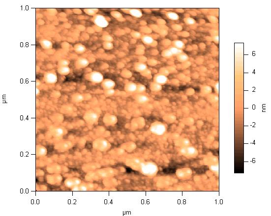
10 where = 1.54 Å is the wavelength of the Cu K source, the width of the peak at half maximum, and the peak position. Gaussian fitting of the Ru (002) peak o gave and the grain size was calculated to be 25 nm after correcting for the X- ray instrument broadening. These diffraction studies show the film is not strongly oxidized during deposition, which excludes mechanism (3) and suggests that the recombinative desorption of oxygen is the dominant mechanism. Atomic force microscope (AFM) images (figure 9a-c) of Ru films (~30nm) deposited at 325 o C show the grain size increases with O 2 exposure. Without O 2 as coreactant, the grains are uniformly small, which produces relatively smooth films with root mean square (RMS) roughness ~1.5 nm for a ~30 nm film. After introducing O 2, some grains grow bigger and the size distribution becomes non-uniform. When E O is approaching E max, the grain size has a narrower distribution and the crystallinity is improved. The RMS value versus E O is summarized in figure 9d. The roughness increases from nm to nm due to the improved crystallinity achieved under higher O 2 exposure. Figure 10a shows that both the resistivity and density of ~30 nm Ru films depend on the O 2 exposure. At low exposure (e.g. E 0.02 Torr s at 325 o C), the film density is O around 7 8 g/cm 3. The density quickly increases with E O and reaches a plateau around the bulk density (12.3 g/cm 3 ) at E O ~ 0.33 Torr s. The film resistivity is more sensitive to O 2 exposure and sharply decreases from 320 cm to 14 cm with E O from zero to Torr s. Further increasing E O to Torr s decreases the resistivity to 9.4 9
11 cm, which is 32% higher than the bulk resistivity (7.1 cm). The thin film resistivity is affected by scattering from GBs, impurities, interfaces and surfaces. [19] Because the grain size is approximately equal to the film thickness, the scatteringinduced-resistivity model can be simplified as: [19] t 0 0 1, [3] t where is the thin film resistivity, 0 the bulk resistivity including the effect of impurity scattering, t 0 the characteristic length related to the electron mean free path and scattering effects of GBs, interfaces and surfaces, and t the film thickness. By linear fitting to 1/t (figure 10b), we got cm and t 0 6 nm. Thus the resistivity for thick films is extrapolated to be 8.6 cm, which is 21% higher than the bulk value. Assuming that both C and O have same scattering effect, the rate of the resistivity increase for these impurities can be estimated to be ~2 cm/at.%, which is close to the value for bulk Cu (1 cm/at.%). [19, 20] The deposition temperature has a less pronounced effect than O 2 exposure. The maximum O 2 exposure for adherent films ( E max ) increases with the deposition temperature, shown in figure 11a. The growth rate increases from 0.5 Å/cycle at 300 o C to 1.7 Å/cycle at 400 o C (figure 11b). The increase of E max with temperature is clearly related to the high growth rate at high temperature, i.e. more Ru precursor molecules can consume more adsorbed oxygen and lower the oxygen concentration in Ru films. Saturation of the growth rate with increasing temperature was also observed for the 10
12 Ru(thd) 3 and RuCp 2 systems, which suggests these ALD processes follow a reaction mechanism similar to the one discussed by T. Aaltonen et al.: Ru films are deposited by oxidizing the precursor ligands with dissociatively adsorbed oxygen from the subsurface region. [4, 6] The resistivity is near 10 cm for deposition temperatures from 320 o C to 400 o C (figure 11b). Figure 12 shows the AFM image of a 35 nm Ru film deposited at 400 o C. Both the roughness (1.9 nm) and crystallinity are similar to the film deposited at 325 o C (figure 8c). Conclusions High quality ruthenium thin films were deposited by ALD with bis(n,n -di-tertbutylacetamidinato)ruthenium(ii) dicarbonyl and O 2. The film crystallinity, density, and resistivity strongly depend on the O 2 exposure, while the roughness is relatively insensitive to E O. As E E, the films have the lowest resistivity, highest density and O max best crystallinity ( ~10 cm, ~12.3 g/cm 3 and grain size comparable to film thickness). High deposition temperature leads to higher growth rate, but has less effect on the film structures and properties. For deposition temperature range of 320 o C 400 o C, the resistivity is ~10 cm and roughness is ~2 nm for 30 nm films. When E E, films O max peel off from the substrate due to the recombinative desorption of O 2. The impurities are mainly O (0.27±0.03 at.%) and C (0.30±0.05 at.%). The C is mostly segregated along grain boundaries, which are less dense than the grain interiors. The O is more uniformly dissolved in the Ru film. The rate of resistivity increase with impurities is estimated to be ~2 cm/at.%, which is comparable to the value of copper (1 cm/at.%). Experimental 11
13 Ru thin films were deposited in a home-built flow-type tube reactor operated at the base pressure 300 mtorr with bis(n,n -di-tert-butylacetamidinato)ruthenium(ii) dicarbonyl and O 2. The substrate temperature was measured by a thermal couple inside the sample holder. The Ru precursor was kept in a glass bubbler at 140 o C and delivered to the reactor by N 2 carrier gas added to the head space of the bubbler to a pressure of about 10 Torr. This added N2 carrier gas, along with the entrained Ru precursor vapor, was released to the reactor in each ALD cycle. High purity O 2 (99.99%) was used as coreactant and delivered from a 5 ml trap volume with its pressure controlled by an inline regulator. One ALD cycle consisted of one Ru precursor dose and one O 2 dose with 10 s purging in between. The deposition temperatures varied from 300 o C to 400 o C. All films were deposited on thermal SiO 2 (300nm) /Si wafers (1 inch by 1.5 inch) with 5 min UV/Ozone pre-treatment to remove surface organic contamination. The film resistivity was calculated from the thickness measured by X-ray reflectivity (XRR) (Scintag XDS2000) multiplying the sheet resistance measured by a four-point probe. The morphology was studied by scanning electron microscope (Zeiss FESEM Ultra55) and atomic force microscopy (Asylum MFP-3D). The crystal structure and phase were determined by X-ray diffraction (Scintag XDS2000) and electron diffraction (JEOL 2100). The roughness and crystallinity were characterized using AFM and transmission electron microscopy (JEOL 2100). The impurity concentrations and their distribution in the crystallites were measured by an atomic probe microscope (LEAP 3000X HR). Impurity analysis was also attempted by X-ray photoelectron spectroscopy (XPS ESCA SSX-100). The ALD Ru film density was obtained from the area density by Rutherford back scattering divided by the film thickness from XRR. 12
14 Figure Captions Figure 1. The dependence of Ru thin film growth rate on the O 2 exposure at the deposition temperature of 325 o C. Figure 2. (a) ED and (b) Cross-sectional TEM image of Ru film / Si deposited at 325 o C with O 2 as co-reactant. Figure 3. (a) XPS spectra (Al K radiation, hv ev ) of a 30nm Ru thin film with low energy (3 kev) Ar + sputtering for 0 s, 30 s and 100 s. (b) High resolution XPS spectrum of O1s after 30 s Ar + sputtering. Figure 4. (a) Cross-sectional TEM image of the film stack on a planar SiO 2 /Si substrate; (b) SEM image of the pre-sharpened micro-tip. Figure 5. The 3D mapping of Ru atoms. Figure 6. (a) The elemental depth profiles across the Co4N / Ru interface. (b) the details of impurity distribution across the interface. Figure 7. The 2D atom mappings of (a) Ru and (b) C. In (b), box A and B indicate the area for local impurity concentration calculation. The line in (b) indicates the profiling location. (c) The C and O line profile across the GB. Figure 8. (a) low and (b) high magnification SEM images and (c) grazing angle XRD spectrum of Ru thin film deposited at 325 o C and E 0.04 Torr s. O 13
15 Figure 9. AFM images of ~30nm Ru thin films deposited at 325 o C with different O 2 exposures: (a) 0 Torr s; (b) Torr s; and (c) Torr s. (d) Summary of the RMS roughness versus O 2 exposure. Figure 10. (a) Resistivity and density variation with O 2 exposure for ALD films deposited at 325 o C; (b) the thickness dependence of resistivity. Figure 11. (a) The maximum O 2 exposure at different deposition temperatures; (b) the growth rate and resistivity of ~30nm Ru films deposited at temperatures. E max and different deposition Figure 12. AFM image of a 35nm Ru thin film deposited at 400 o C and roughness is 1.9 nm. E max. The RMS Table Table 1. Comparison of the lattice spacings of rutile RuO 2 (PCPDF File No ), hexagonal Ru (PCPDF File No ) and measurements from ED. Rutile RuO 2 Hexagonal Ru ED plane d-spacing (Å) plane d-spacing (Å) d-spacing (Å) (110) (100) (101) (002) (200) (101) (111) (102) (210) (110) (211) (103)
16 References [1] V. Misra, G. Lucovsky and G. Parsons, MRS Bull. 2002, 27, 212. [2] O. K. Kwon, J. H. Kim, H. S. Park and S. W. Kang, J. Electrochem. Soc. 2004, 151, G109. [3] S. K. Kim, G. J. Choi, S. Y. Lee, M. Seo, S. W. Lee, J. H. Han, H. S. Ahn, S. Han and C. S. Hwang, Adv. Mater. 2008, 20, [4] T. Aaltonen, A. Rahtu, M. Ritala and M. Leskela, Electrochem. Solid State Lett. 2003, 6, C130. [5] T. Aaltonen, P. Alen, M. Ritala and M. Leskela, Chem. Vapor Depos. 2003, 9, 45. [6] T. Aaltonen, M. Ritala, K. Arstila, J. Keinonen and M. Leskela, Chem. Vapor Depos. 2004, 10, 215. [7] H. Z. Li, T. Aaltonen, Z. W. Li, B. S. Lim and R. G. Gordon, The Open Inorganic Chemistry Journal 2008, 2, 11. [8] H. Li, D. B. Farmer, R. G. Gordon, Y. Lin and J. Vlassak, J. Electrochem. Soc. 2007, 154, D642. [9] S. H. Kwon, O. K. Kwon, J. H. Kim, S. J. Jeong, S. W. Kim and S. W. Kang, J. Electrochem. Soc. 2007, 154, H773. [10] H. Over and A. P. Seitsonen, Science 2002, 297,
17 [11] B. Gault, F. de Geuser, L. T. Stephenson, M. P. Moody, B. C. Muddle and S. P. Ringer, Microsc. Microanal. 2008, 14, 296. [12] D. N. Seidman, Ann. Rev. Mater. Res. 2007, 37, 127. [13] Y. D. Kim, H. Over, G. Krabbes and G. Ertl, Top. Catal. 2001, 14, 95. [14] A. Bottcher and H. Niehus, J. Chem. Phys. 1999, 110, [15] R. Blume, H. Niehus, H. Conrad, A. Bottcher, L. Aballe, L. Gregoratti, A. Barinov and M. Kiskinova, J. Phys. Chem. B 2005, 109, [16] A. Bottcher, H. Conrad and H. Niehus, J. Chem. Phys. 2000, 112, [17] S. J. Park, W. H. Kim, W. J. Maeng, Y. S. Yang, C. G. Park, H. Kim, K. N. Lee, S. W. Jung and W. K. Seong, Thin Solid Films 2008, 516, [18] B. E. Warren, X-Ray Diffraction, Dover Publications, INC., New York [19] S. M. Rossnagel and T. S. Kuan, J. Vac. Sci. Technol. B 2004, 22, 240. [20] J. M. E. Harper, E. G. Colgan, C. K. Hu, J. P. Hummel, L. P. Buchwalter and C. E. Uzoh, MRS Bull. 1994, 19,
18 Figures Growth Rate (Å/cycle) O 2 Exposure (Torr s) Figure 1. The dependence of Ru thin film growth rate on the O 2 exposure at the deposition temperature of 325 o C. 17
 (002)")
 (103)")
 ED and")


19 Si (200) Ru (100) (002) (101) (102) (110) (103) (a) (b) Figure 2. (a) ED and (b) Cross-sectional TEM image of Ru film / Si deposited at 325 o C with O 2 as co-reactant. 18
20 O1s Ru3d 1 Ru3p 0.8 O1s Ru3s s Ru4p Ru4s Ru4d s 0 100s Binding Energy (ev) (a) 1.5 O1s Binding Energy (ev) (b) Figure 3. (a) XPS spectra (Al K radiation, hv ev ) of a 30nm Ru thin film with low energy (3 kev) Ar + sputtering for 0 s, 30 s and 100 s. (b) High resolution XPS spectrum of O1s after 30 s Ar + sputtering. 19
 Cross-sectional TEM image of the film")

21 Co 4 N Ru WN SiO 2 5 nm (a) (b) Figure 4. (a) Cross-sectional TEM image of the film stack on a planar SiO 2 /Si substrate; (b) SEM image of the pre-sharpened micro-tip. 20


22 Figure 5. The 3D mapping of Ru atoms. 21
23 100 Atom% Co N O C Ru Distance (nm) (a) 2 Co N O C Ru Atom% Distance (nm) (b) Figure 6. (a) The elemental depth profiles across the Co 4 N / Ru interface. (b) the details of impurity distribution across the interface. 22
24 (a) (b) 23
25 C O (c) Figure 7. The 2D atom mappings of (a) Ru and (b) C. In (b), boxes A and B indicate the areas for local impurity concentration measurements. The line in (b) indicates the profiling location. (c) The C and O line profile across the GB. 24


26 (a) (b) 25
27 (002) Hexgonal Ru Rutile RuO 2 Intensity I (a.u.) (100) (200) (101) ( o ) (c) Figure 8. (a) low and (b) high magnification SEM images and (c) grazing angle XRD spectrum of Ru thin film deposited at 325 o C and E E 0.04 Torr s. O max 26

28 (a) (b) 27
 (d) 28")
29 (c) Roughness (nm) O 2 Exposure (Torr s) (d) 28
30 Figure 9. AFM images of ~30nm Ru thin films deposited at 325 o C with different O 2 exposures: (a) 0 Torr s; (b) Torr s; and (c) Torr s. (d) Summary of the RMS roughness versus O 2 exposure. 29
31 Bulk density 12.3g/cm Resistivity ( cm) cm 2 Bulk resistivity 7.1 cm O 2 Exposure (Torr s) Density (g/cm 3 ) (a) Resistivity ( cm) = 8.6 ( / t ) cm 21% higher than the bulk ( 0 = 7.1 cm) /t (nm -1 ) (b) Figure 10. (a) Resistivity and density variation with O 2 exposure for ALD films with thickness ~35nm deposited at 325 o C; (b) the thickness dependence of resistivity. 30
32 Max O 2 Exposure (Torr s) Temperature ( o C) (a) Growth Rate (Å/cycle) Resistivity ( cm) Temperature ( o C) (b) Figure 11. (a) The maximum O 2 exposure at different deposition temperatures; (b) the growth rate and resistivity of ~30nm Ru films deposited at temperatures. E max and different deposition 31

33 Figure 12. AFM image of a 35nm Ru thin film deposited at 400 o C and RMS roughness is 1.9 nm. E max. The 32
Smooth, Low-Resistance, Pinhole-free, Conformal Ruthenium Films by Pulsed Chemical Vapor Deposition
 Smooth, Low-Resistance, Pinhole-free, Conformal Ruthenium Films by Pulsed Chemical Vapor Deposition The Harvard community has made this article openly available. Please share how this access benefits you.
ALD and CVD of Copper-Based Metallization for. Microelectronic Fabrication. Department of Chemistry and Chemical Biology
 ALD and CVD of Copper-Based Metallization for Microelectronic Fabrication Yeung Au, Youbo Lin, Hoon Kim, Zhengwen Li, and Roy G. Gordon Department of Chemistry and Chemical Biology Harvard University Introduction
11:30 AM - C4.4 Chemical Vapor Deposition of Cobalt Nitride and Its Application as an Adhesion-enhancing Layer for Advanced Copper Interconnects
 2012-04-11 SYMPOSIUM C 11:30 AM - C4.4 Chemical Vapor Deposition of Cobalt Nitride and Its Application as an Adhesion-enhancing Layer for Advanced Copper Interconnects Jing Yang 1, Harish B. Bhandari 1,
ALD of Manganese Silicate
 ALD of Manganese Silicate Roy G. Gordon, 1,2 * Lu Sun, 2 Qiang Chen, 3 Jin-Seong Park 4 and Sang Bok Kim 1 1 Department of Chemistry and Chemical Biology 2 School of Engineering and Applied Sciences, Cambridge,
A New Liquid Precursor for Pure Ruthenium Depositions. J. Gatineau, C. Dussarrat
 1.1149/1.2727414, The Electrochemical Society A New Liquid Precursor for Pure Ruthenium Depositions J. Gatineau, C. Dussarrat Air Liquide Laboratories, Wadai 28, Tsukuba city, Ibaraki Prefecture, 3-4247,
Eindhoven University of Technology MASTER. Atomic layer deposition of Ruthenium thin films using oxygen. Verkuijlen, R.O.F.
 Eindhoven University of Technology MASTER Atomic layer deposition of Ruthenium thin films using oxygen Verkuijlen, R.O.F. Award date: 2009 Link to publication Disclaimer This document contains a student
DEPOSITION AND CHARACTERISTICS OF TANTALUM NITRIDE FILMS BY PLASMA ASSISTED ATOMIC LAYER DEPOSITION AS CU DIFFUSION BARRIER
 Mat. Res. Soc. Symp. Proc. Vol. 766 2003 Materials Research Society E3.22.1 DEPOSITION AND CHARACTERISTICS OF TANTALUM NITRIDE FILMS BY PLASMA ASSISTED ATOMIC LAYER DEPOSITION AS CU DIFFUSION BARRIER Kyoung-Il
Microstructure, morphology and their annealing behaviors of alumina films synthesized by ion beam assisted deposition
 Nuclear Instruments and Methods in Physics Research B 206 (2003) 357 361 www.elsevier.com/locate/nimb Microstructure, morphology and their annealing behaviors of alumina films synthesized by ion beam assisted
Ruthenium Oxide Films Prepared by Reactive Biased Target Sputtering
 Ruthenium Oxide Films Prepared by Reactive Biased Target Sputtering Hengda Zhang Anthony Githinji 1. Background RuO2 in both crystalline and amorphous forms is of crucial importance for theoretical as
Characterization of Nanoscale Electrolytes for Solid Oxide Fuel Cell Membranes
 Characterization of Nanoscale Electrolytes for Solid Oxide Fuel Cell Membranes Cynthia N. Ginestra 1 Michael Shandalov 1 Ann F. Marshall 1 Changhyun Ko 2 Shriram Ramanathan 2 Paul C. McIntyre 1 1 Department
ALD of Scandium Oxide from Tris(N,N -diisopropylacetamidinato)scandium and Water
scandium and Water") ALD of Scandium Oxide from Tris(N,N -diisopropylacetamidinato)scandium and Water Philippe P. de Rouffignac, Roy G. Gordon Dept. of Chemistry,, Cambridge, MA gordon@chemistry.harvard.edu (617) 495-4017
ALD of Scandium Oxide from Tris(N,N -diisopropylacetamidinato)scandium and Water Philippe P. de Rouffignac, Roy G. Gordon Dept. of Chemistry,, Cambridge, MA gordon@chemistry.harvard.edu (617) 495-4017
Deposited by Sputtering of Sn and SnO 2
 Journal of the Korean Ceramic Society Vol. 49, No. 5, pp. 448~453, 2012. http://dx.doi.org/10.4191/kcers.2012.49.5.448 Comparative Study of Nitrogen Incorporated SnO 2 Deposited by Sputtering of Sn and
Low Temperature Atomic Layer Deposition of Tin Dioxide, SnO\(_2\)
") Low Temperature Atomic Layer Deposition of Tin Dioxide, \(_2\) The arvard community has made this article openly available. Please share how this access benefits you. Your story matters Citation eo, Jaeyeong,
Low Temperature Atomic Layer Deposition of Tin Dioxide, \(_2\) The arvard community has made this article openly available. Please share how this access benefits you. Your story matters Citation eo, Jaeyeong,
Silver Diffusion Bonding and Layer Transfer of Lithium Niobate to Silicon
 Chapter 5 Silver Diffusion Bonding and Layer Transfer of Lithium Niobate to Silicon 5.1 Introduction In this chapter, we discuss a method of metallic bonding between two deposited silver layers. A diffusion
Supporting Information
 Supporting Information Large-Area, Transfer-Free, Oxide-Assisted Synthesis of Hexagonal Boron Nitride Films and Their Heterostructures with MoS2 and WS2 Sanjay Behura, Phong Nguyen, Songwei Che, Rousan
ALD of Copper and Copper Oxide Thin Films for Applications in Metallization Systems of ULSI Devices
 ALD of Copper and Copper Oxide Thin Films for Applications in Metallization Systems of ULSI Devices a, Steffen Oswald b, Nina Roth c, Heinrich Lang c, Stefan E. Schulz a,d, and Thomas Gessner a,d a Center
Metallorganic Chemical Vapor Deposition of Ru Films Using Cyclopentadienyl-Propylcyclopentadienylruthenium II and Oxygen
 0013-4651/2002/149 6 /C317/7/$7.00 The Electrochemical Society, Inc. Metallorganic Chemical Vapor Deposition of Ru Films Using Cyclopentadienyl-Propylcyclopentadienylruthenium II and Oxygen Sang Yeol Kang,
Growth Of TiO 2 Films By RF Magnetron Sputtering Studies On The Structural And Optical Properties
 Journal of Multidisciplinary Engineering Science and Technology (JMEST) Growth Of TiO 2 Films By RF Magnetron Sputtering Studies On The Structural And Optical Properties Ahmed K. Abbas 1, Mohammed K. Khalaf
Supporting Information. Solution-Processed 2D PbS Nanoplates with Residual Cu 2 S. Exhibiting Low Resistivity and High Infrared Responsivity
 Supporting Information Solution-Processed 2D PbS Nanoplates with Residual Cu 2 S Exhibiting Low Resistivity and High Infrared Responsivity Wen-Ya Wu, Sabyasachi Chakrabortty, Asim Guchhait, Gloria Yan
Low Thermal Budget NiSi Films on SiGe Alloys
 Mat. Res. Soc. Symp. Proc. Vol. 745 2003 Materials Research Society N6.6.1 Low Thermal Budget NiSi Films on SiGe Alloys S. K. Ray 1,T.N.Adam,G.S.Kar 1,C.P.SwannandJ.Kolodzey Department of Electrical and
EFFECT OF GROWTH TEMPERATURE ON THE CATALYST-FREE GROWTH OF LONG SILICON NANOWIRES USING RADIO FREQUENCY MAGNETRON SPUTTERING
 International Journal of Nanoscience Vol. 10, Nos. 1 & 2 (2011) 13 17 #.c World Scienti c Publishing Company DOI: 10.1142/S0219581X11007594 EFFECT OF GROWTH TEMPERATURE ON THE CATALYST-FREE GROWTH OF LONG
Fabrication of MoS 2 Thin Film Transistors via Novel Solution Processed Selective Area Deposition
 Electronic Supplementary Material (ESI) for Journal of Materials Chemistry C. This journal is The Royal Society of Chemistry 2015 Supplementary Information Fabrication of MoS 2 Thin Film Transistors via
Supporting Information
 Supporting Information Controlled Vapor Phase Growth of Single Crystalline, Two-Dimensional GaSe Crystals with High Photoresponse Xufan Li, Ming-Wei Lin, Alexander A. Puretzky, Juan C. Idrobo, Cheng Ma,
SUPPLEMENTARY INFORMATION
 doi:10.1038/nature11562 Figure S1 Distinction of graphene and copper grain boundaries. a-b, SEM images of oxidised graphene/cu at different magnifications. The white dotted lines indicate the oxidised
X-ray Photoelectron Spectroscopy
 X-ray Photoelectron Spectroscopy X-ray photoelectron spectroscopy (XPS) is a non-destructive technique used to analyze the elemental compositions, chemical and electronic states of materials. XPS has a
Precursors with Metal-Nitrogen Bonds for ALD of Metals, Nitrides and Oxides
 Precursors with Metal-Nitrogen Bonds for ALD of Metals, Nitrides and Oxides Abstract Roy Gordon Gordon@chemistry.harvard.edu, Cambridge, MA To achieve ALD s unique characteristics, ALD precursors must
Supplementary Information
 Supplementary Information Supplementary Figure 1 Characterization of precursor coated on salt template. (a) SEM image of Mo precursor coated on NaCl. Scale bar, 50 μm. (b) EDS of Mo precursor coated on
Polycrystalline and microcrystalline silicon
 6 Polycrystalline and microcrystalline silicon In this chapter, the material properties of hot-wire deposited microcrystalline silicon are presented. Compared to polycrystalline silicon, microcrystalline
Growth and Doping of SiC-Thin Films on Low-Stress, Amorphous Si 3 N 4 /Si Substrates for Robust Microelectromechanical Systems Applications
 Journal of ELECTRONIC MATERIALS, Vol. 31, No. 5, 2002 Special Issue Paper Growth and Doping of SiC-Thin Films on Low-Stress, Amorphous Si 3 N 4 /Si Substrates for Robust Microelectromechanical Systems
Thin, Continuous, and Conformal Copper Films by Reduction of Atomic Layer Deposited Copper Nitride**
 DOI: 1.12/cvde.266485 Full Paper Thin, Continuous, and Conformal Copper Films by Reduction of Atomic Layer Deposited Copper itride** By Zhengwen Li and Roy G. Gordon* Thin and continuous copper films serve
Synthesis and Characterization of DC Magnetron Sputtered ZnO Thin Films Under High Working Pressures
 Accepted Manuscript Synthesis and Characterization of DC Magnetron Sputtered ZnO Thin Films Under High Working Pressures M. Hezam, N. Tabet, A. Mekki PII: S0040-6090(10)00417-7 DOI: doi: 10.1016/j.tsf.2010.03.091
arxiv:cond-mat/ v2 [cond-mat.mtrl-sci] 29 Nov 2003
![arxiv:cond-mat/ v2 [cond-mat.mtrl-sci] 29 Nov 2003](/thumbs/93/114120274.jpg "arxiv:cond-mat/ v2 [cond-mat.mtrl-sci] 29 Nov 2003") Fabrication and Electrical Properties of Pure Phase Films B. G. Chae, D. H. Youn, H. T. Kim, S. Maeng, and K. Y. Kang Basic Research Laboratory, ETRI, Daejeon 305-350, Republic of Korea arxiv:cond-mat/0311616v2
Fabrication and Electrical Properties of Pure Phase Films B. G. Chae, D. H. Youn, H. T. Kim, S. Maeng, and K. Y. Kang Basic Research Laboratory, ETRI, Daejeon 305-350, Republic of Korea arxiv:cond-mat/0311616v2
Nucleation and growth of nanostructures and films. Seongshik (Sean) Oh
 Oh") Nucleation and growth of nanostructures and films Seongshik (Sean) Oh Outline Introduction and Overview 1. Thermodynamics and Kinetics of thin film growth 2. Defects in films 3. Amorphous, Polycrystalline
Nucleation and growth of nanostructures and films Seongshik (Sean) Oh Outline Introduction and Overview 1. Thermodynamics and Kinetics of thin film growth 2. Defects in films 3. Amorphous, Polycrystalline
Microstructure and Vacuum Leak Characteristics of SiC coating Layer by Three Different Deposition Methods
 Microstructure and Vacuum Leak Characteristics of SiC coating Layer by Three Different Deposition Methods Y. Kim Professor, Department of Materials Science and Engineering, College of Engineering, Kyonggi
In-situ Monitoring of Atomic Layer Deposition Processes
 Faculty of Electrical and Computer Engineering - Institute of Semiconductors and Microsystems NanoZEIT seminar @ SEMICON 2011 Deposition Processes M. Knaut*, M. Junige, M. Geidel, M. Albert, and J. W.
Supporting Information
 Copyright WILEY VCH Verlag GmbH & Co. KGaA, 69469 Weinheim, Germany, 2012. Supporting Information for Small, DOI: 10.1002/smll. 201102654 Large-Area Vapor-Phase Growth and Characterization of MoS 2 Atomic
High-Resolution, Electrohydrodynamic Inkjet Printing of Stretchable, Metal Oxide Semiconductor Transistors with High Performances
 Electronic Supplementary Material (ESI) for Nanoscale. This journal is The Royal Society of Chemistry 2016 ` Electronic Supplementary Information High-Resolution, Electrohydrodynamic Inkjet Printing of
Supplementary Figure S1 Photograph of MoS 2 and WS 2 flakes exfoliated by different metal naphthalenide (metal = Na, K, Li), and dispersed in water.
, and dispersed in water.") Supplementary Figure S1 Photograph of MoS 2 and WS 2 flakes exfoliated by different metal naphthalenide (metal = Na, K, Li), and dispersed in water. Supplementary Figure S2 AFM measurement of typical LTMDs
Supplementary Figure S1 Photograph of MoS 2 and WS 2 flakes exfoliated by different metal naphthalenide (metal = Na, K, Li), and dispersed in water. Supplementary Figure S2 AFM measurement of typical LTMDs
Pre-treatment of low temperature GaN buffer layer deposited on AlN Si substrate by hydride vapor phase epitaxy
 Ž. Surface and Coatings Technology 131 000 465 469 Pre-treatment of low temperature GaN buffer layer deposited on AlN Si substrate by hydride vapor phase epitaxy Ha Jin Kim, Ho-Sun Paek, Ji-Beom Yoo Department
Application of ultra-thin aluminum oxide etch mask made by atomic layer deposition technique
 IOP Publishing Journal of Physics: Conference Series 61 (2007) 369 373 doi:10.1088/1742-6596/61/1/074 International Conference on Nanoscience and Technology (ICN&T 2006) Application of ultra-thin aluminum
Properties of TiN thin films grown on SiO 2 by reactive HiPIMS
 Properties of TiN thin films grown on SiO 2 by reactive HiPIMS Friðrik Magnus 1, Árni S. Ingason 1, Ólafur B. Sveinsson 1, S. Shayestehaminzadeh 1, Sveinn Ólafsson 1 and Jón Tómas Guðmundsson 1,2 1 Science
Electron backscattered diffraction study of poly-si by Ni-mediated crystallization of amorphous silicon using a SiO 2 nanocap
 Electron backscattered diffraction study of poly-si by Ni-mediated crystallization of amorphous silicon using a SiO 2 nanocap Y. J. Chang, a) J. H. Oh, K. H. Kim, and Jin Jang b) Advanced Display Research
Supplementary Figure 1 In situ QCM measurements of Pd ALD on different oxide
 Supplementary Figure 1 In situ QCM measurements of Pd ALD on different oxide surfaces using either HCHO or H 2 as reducing agent at 150 ºC. (a) On Al 2 O 3 ; (b) on ZrO 2 ; (c), on TiO 2. See Supplementary
High Density Plasma Etching of IrRu Thin Films as a New Electrode for FeRAM
 Integrated Ferroelectrics, 84: 169 177, 2006 Copyright Taylor & Francis Group, LLC ISSN 1058-4587 print / 1607-8489 online DOI: 10.1080/10584580601085750 High Density Plasma Etching of IrRu Thin Films
Enhancement of Copper Wetting via Surfactant-Based Post-Treatment of Ultra-Thin Atomic Layer Deposited Tantalum Nitride Liners
 Mat. Res. Soc. Symp. Proc. Vol. 766 2003 Materials Research Society E10.3.1 Enhancement of Copper Wetting via Surfactant-Based Post-Treatment of Ultra-Thin Atomic Layer Deposited Tantalum Nitride Liners
With the increasing of the use of polymers in the microelectronic industry,
 CHAPTER SEVEN INTERFACIAL ADHESION BETWEEN THE PI/TiO 2 NANO HYBRID FILMS AND COPPER SYSTEM Summary With the increasing of the use of polymers in the microelectronic industry, adequate adhesion between
Supplimentary Information. Large-Scale Synthesis and Functionalization of Hexagonal Boron Nitride. Nanosheets
 Electronic Supplementary Material (ESI) for Nanoscale. This journal is The Royal Society of Chemistry 2014 Supplimentary Information Large-Scale Synthesis and Functionalization of Hexagonal Boron Nitride
CHAPTER 4. SYNTHESIS OF ALUMINIUM SELENIDE (Al 2 Se 3 ) NANO PARTICLES, DEPOSITION AND CHARACTERIZATION
 NANO PARTICLES, DEPOSITION AND CHARACTERIZATION") 40 CHAPTER 4 SYNTHESIS OF ALUMINIUM SELENIDE (Al 2 Se 3 ) NANO PARTICLES, DEPOSITION AND CHARACTERIZATION 4.1 INTRODUCTION Aluminium selenide is the chemical compound Al 2 Se 3 and has been used as a precursor
40 CHAPTER 4 SYNTHESIS OF ALUMINIUM SELENIDE (Al 2 Se 3 ) NANO PARTICLES, DEPOSITION AND CHARACTERIZATION 4.1 INTRODUCTION Aluminium selenide is the chemical compound Al 2 Se 3 and has been used as a precursor
Platypus Gold Coated Substrates. Bringing Science to the Surface
 Platypus Gold Coated Substrates Bringing Science to the Surface Overview Gold Coated Substrates - Gold Coating Introduction - Glossary of Terms - Gold Coating Methods - Critical Features Platypus Gold
Deposition and characterization of sputtered ZnO films
 Superlattices and Microstructures 42 (2007) 89 93 www.elsevier.com/locate/superlattices Deposition and characterization of sputtered ZnO films W.L. Dang, Y.Q. Fu, J.K. Luo, A.J. Flewitt, W.I. Milne Electrical
Characteristics of Cobalt Films Deposited by Using a Remote Plasma ALD Method with a CpCo(CO) 2 Precursor
 2 Precursor") Journal of the Korean Physical Society, Vol. 50, No. 4, April 2007, pp. 1141 1146 Characteristics of Cobalt Films Deposited by Using a Remote Plasma ALD Method with a CpCo(CO) 2 Precursor Keunwoo Lee,
Journal of the Korean Physical Society, Vol. 50, No. 4, April 2007, pp. 1141 1146 Characteristics of Cobalt Films Deposited by Using a Remote Plasma ALD Method with a CpCo(CO) 2 Precursor Keunwoo Lee,
Supplementary Figure 1. (a-d). SEM images of h-bn film on iron foil with corresponding Raman spectra. Iron foil was reused for re-growth of h-bn
. SEM images of h-bn film on iron foil with corresponding Raman spectra. Iron foil was reused for re-growth of h-bn") Supplementary Figure 1. (a-d). SEM images of h-bn film on iron foil with corresponding Raman spectra. Iron foil was reused for re-growth of h-bn after bubbling transfer. Scale bars (ad) 20 μm. Supplementary
Supplementary Figure 1. (a-d). SEM images of h-bn film on iron foil with corresponding Raman spectra. Iron foil was reused for re-growth of h-bn after bubbling transfer. Scale bars (ad) 20 μm. Supplementary
ITO. Crystal structure: Cubic, space group Ia3 No. 206, ci80, a = nm, Z = 16
 ITO Indium tin oxide (ITO) is a ternary composition of indium, tin and oxygen in varying proportions. Depending on the oxygen content, it can either be described as a ceramic or alloy. Indium tin oxide
ALD TiO 2 coated Silicon Nanowires for Lithium Ion Battery Anodes with enhanced Cycling Stability and Coulombic Efficiency
 ALD TiO 2 coated Silicon Nanowires for Lithium Ion Battery Anodes with enhanced Cycling Stability and Coulombic Efficiency Elmira Memarzadeh Lotfabad a, Peter Kalisvaart a,*, Kai Cui b, Alireza Kohandehghan
Chapter 3 Silicon Device Fabrication Technology
 Chapter 3 Silicon Device Fabrication Technology Over 10 15 transistors (or 100,000 for every person in the world) are manufactured every year. VLSI (Very Large Scale Integration) ULSI (Ultra Large Scale
Mechanical Properti es of ZnO:Mo Transparent Conducting Oxide Thin Film Prepared by Sputtering
 CHINESE JOURNAL OF PHYSICS VOL. 51, NO. 3 June 2013 Mechanical Properti es of ZnO:Mo Transparent Conducting Oxide Thin Film Prepared by Sputtering Y. C. Lin, C. C. Chen, and W. Y. Lai Department of Mechatronics
CHAPTER 3. Experimental Results of Magnesium oxide (MgO) Thin Films
 Thin Films") CHAPTER 3 Experimental Results of Magnesium oxide (MgO) Thin Films Chapter: III ---------------------------------------------------------------- Experimental Results of Magnesium oxide (MgO) Thin Films
CHAPTER 3 Experimental Results of Magnesium oxide (MgO) Thin Films Chapter: III ---------------------------------------------------------------- Experimental Results of Magnesium oxide (MgO) Thin Films
Fundamentals of X-ray diffraction and scattering
 Fundamentals of X-ray diffraction and scattering Don Savage dsavage@wisc.edu 1231 Engineering Research Building (608) 263-0831 X-ray diffraction and X-ray scattering Involves the elastic scattering of
CEMS study on diluted magneto titanium oxide films prepared by pulsed laser deposition
 Hyperfine Interact (2006) 168:1065 1071 DOI 10.1007/s10751-006-9406-2 CEMS study on diluted magneto titanium oxide films prepared by pulsed laser deposition K. Nomura & K. Inaba & S. Iio & T. Hitosugi
Supporting Information
 Supporting Information Vapor-Phase Atomic-Controllable Growth of Amorphous Li 2 S for High-Performance Lithium-Sulfur Batteries Xiangbo Meng, David J. Comstock, Timothy T. Fister, and Jeffrey W. Elam *
ATOMIC LAYER DEPOSITION OF 2D TRANSITION METAL DICHALOGENIDES
 ATOMIC LAYER DEPOSITION OF 2D TRANSITION METAL DICHALOGENIDES Annelies Delabie, M. Caymax, B. Groven, M. Heyne, K. Haesevoets, J. Meersschaut, T. Nuytten, H. Bender, T. Conard, P. Verdonck, S. Van Elshocht,
Pulsed Nucleation Layer of Tungsten Nitride Barrier Film and its Application in DRAM and Logic Manufacturing
 Pulsed Nucleation Layer of Tungsten Nitride arrier Film and its Application in DRAM and Logic Manufacturing Kaihan Ashtiani, Josh Collins, Juwen Gao, Xinye Liu, Karl Levy Novellus Systems, Inc. 4 N. First
Selective atomic layer deposition of zirconium oxide on copper patterned silicon substrate
 Selective atomic layer deposition of zirconium oxide on copper patterned silicon substrate Jaya Parulekar, Department of Chemical and Biological Engineering, Illinois Institute of Technology, Chicago,
Optical, microstructural and electrical studies on sol gel derived TiO 2 thin films
 Indian Journal of Pure & Applied Physics Vol. 55, January 2017, pp. 81-85 Optical, microstructural and electrical studies on sol gel derived TiO 2 thin films M Bilal Tahir*, S Hajra, M Rizwan & M Rafique
Development of different copper seed layers with respect to the copper electroplating process
 Microelectronic Engineering 50 (2000) 433 440 www.elsevier.nl/ locate/ mee Development of different copper seed layers with respect to the copper electroplating process a, a a b b b K. Weiss *, S. Riedel,
SUPPLEMENTARY INFORMATION
 High Electrochemical Activity of the Oxide Phase in Model Ceria- and Ceria-Ni Composite Anodes William C. Chueh 1,, Yong Hao, WooChul Jung, Sossina M. Haile Materials Science, California Institute of Technology,
Evaluation of silicon nitride and silicon carbide as efficient polysilicon grain-growth inhibitors
 JOURNAL OF MATERIALS SCIENCE LETTERS 18 (1999)1427 1431 Evaluation of silicon nitride and silicon carbide as efficient polysilicon grain-growth inhibitors C. L. CHA, E. F. CHOR Center For Optoelectronics,
ENCAPSULATION OF ORGANIC LIGHT EMITTING DIODES
 ENCAPSULATION OF ORGANIC LIGHT EMITTING DIODES Bhadri Visweswaran Sigurd Wagner, James Sturm, Electrical Engineering, Princeton University, NJ Siddharth Harikrishna Mohan, Prashant Mandlik, Jeff Silvernail,
Selective Vapor Deposition
 Selective Vapor Deposition The Harvard community has made this article openly available. Please share how this access benefits you. Your story matters. Citation Accessed Citable Link Terms of Use Gordon,
D DAVID PUBLISHING. Dielectric Properties of ZrTiO 4 Thin Films Prepared by Reactive DC Magnetron Co-sputtering. 1. Introduction
 Journal of Physical Science and Application 7 (6) (2017) 24-29 doi: 10.17265/2159-5348/2017.06.004 D DAVID PUBLISHING Dielectric Properties of ZrTiO 4 Thin Films Prepared by Reactive DC Magnetron Co-sputtering
RightCopyright 2006 American Vacuum Soci
 Title Gallium nitride thin films deposite magnetron sputtering Author(s) Maruyama, T; Miyake, H Citation JOURNAL OF VACUUM SCIENCE & (2006), 24(4): 1096-1099 TECHNOL Issue Date 2006 URL http://hdl.handle.net/2433/43541
Supplementary Material. for Low-Power Electronics
 Supplementary Material Chemical Vapor Deposition of Monolayer MoS2 Directly on Ultrathin Al2O3 for Low-Power Electronics Hadallia Bergeron 1, Vinod K. Sangwan 1, Julian J. McMorrow 1, Gavin P. Campbell
Ruthenium and Ruthenium-Dioxide Surface Chemistry. Herbert Over
 Founded 1607 Ruthenium and Ruthenium-Dioxide Surface Chemistry IEUVI Optics TWG Meeting November 10, 2005 Herbert Over Physical Chemistry Department Justus Liebig Universität Gießen TransMIT Centrum for
Large-scale Spinning of Silver Nanofibers as Flexible and. Reliable Conductors
 Supporting Information For Large-scale Spinning of Silver Nanofibers as Flexible and Reliable Conductors Ya Huang 1, Xiaopeng Bai 1, Ming Zhou 2, Suiyang Liao 1, Zongfu Yu 2, Yaping Wang 3 and Hui Wu 1,*
Examples of the use of XPS in Catalysis Research from the Vohs Group
 Examples of the use of XPS in Catalysis Research from the Vohs Group Supported monolayer vanadia catalysts Ceria/zirconia automotive emissions control catalysts Reaction of oxygenates on Zn Pd/Zn methanol
The Effect of Interfacial Roughness on the Electrical Properties of Organic Thin Film Transistors with Anisotropic Dielectric Layer
 Mol. Cryst. Liq. Cryst., Vol. 476, pp. 157=[403] 163=[409], 2007 Copyright # Taylor & Francis Group, LLC ISSN: 1542-1406 print=1563-5287 online DOI: 10.1080/15421400701735673 The Effect of Interfacial
Growth of SiC thin films on graphite for oxidation-protective coating
 Growth of SiC thin films on graphite for oxidation-protective coating J.-H. Boo, a) M. C. Kim, and S.-B. Lee Department of Chemistry, Sungkyunkwan University, Suwon 440-746, Korea S.-J. Park and J.-G.
Characterization of interfacial reactions between ionized metal plasma deposited Al 0.5 wt.% Cu and Ti on SiO 2
 Materials Science and Engineering B56 (2000) 101 105 www.elsevier.com/locate/mseb Characterization of interfacial reactions between ionized metal plasma deposited Al 0.5 wt.% Cu and Ti on SiO 2 Y.K. Lee
Anomaly of Film Porosity Dependence on Deposition Rate
 Anomaly of Film Porosity Dependence on Deposition Rate Stephen P. Stagon and Hanchen Huang* Department of Mechanical Engineering, University of Connecticut, Storrs, CT 06269 J. Kevin Baldwin and Amit Misra
University, Piscataway, New Jersey 08854, USA. Massachusetts 02138, USA
 10.1149/1.2779073 The Electrochemical Society In-situ FTIR Study of Atomic Layer Deposition (ALD) of Copper Metal Films Min Dai a, Jinhee Kwon a, Erik Langereis a, Leszek Wielunski a, Yves J. Chabal a
Hei Wong.
 Defects and Disorders in Hafnium Oxide and at Hafnium Oxide/Silicon Interface Hei Wong City University of Hong Kong Email: heiwong@ieee.org Tokyo MQ2012 1 Outline 1. Introduction, disorders and defects
Area-selective atomic layer deposition for self-aligned fabrication
 Area-selective atomic layer deposition for self-aligned fabrication Adrie Mackus Eindhoven University a.j.m.mackus@tue.nl Area-selective ALD for bottom-up processing Top-down Bottom-up Building technology
UNCORRECTED PROOF ARTICLE IN PRESS. 2 Grain boundary structures of atomic layer deposited TiN. 3 S. Li a, *, C.Q. Sun b, H.S.
 + model 1 Thin Solid Films xx (2005) xxx xxx www.elsevier.com/locate/tsf 2 Grain boundary structures of atomic layer deposited TiN 3 S. Li a, *, C.Q. Sun b, H.S. Park c 4 5 6 7 8 bstract a School of Materials
Characterization of Cu/Cu Bonding Interface Prepared by Surface Activated Bonding at Room Temperature
 Characterization of Cu/Cu Bonding Interface Prepared by Surface Activated Bonding at Room Temperature Jun Utsumi 1, Yuko Ichiyanagi *2 1 Advanced Technology Research Centre, Mitsubishi Heavy Industries,
Supplementary Figure 1. Schematic for the growth of high-quality uniform
 Supplementary Figure 1. Schematic for the growth of high-quality uniform monolayer WS 2 by ambient-pressure CVD. Supplementary Figure 2. Schematic structures of the initial state (IS) and the final state
Surface Pretreatments for Remove of Native Cu Oxide Layer
 Paper Surface Pretreatments for Remove of Native Cu Oxide Layer Hyunjin Ju 1, Yong-Hyuk Lee 2, Youn-Seoung Lee 2, and Sa-Kyun Rha 1 * 1 Department of Materials Engineering, Hanbat National University,
Optically Assisted Metal-Induced Crystallization of Thin Si Films for Low-Cost Solar Cells
 Optically Assisted Metal-Induced Crystallization of Thin Si Films for Low-Cost Solar Cells Wei Chen, Bhushan Sopori, Kim Jones, and Robert Reedy, National Renewable Energy Laboratory, Golden, CO; N. M.
O2 Plasma Damage and Dielectric Recoveries to Patterned CDO Low-k Dielectrics
 O2 Plasma Damage and Dielectric Recoveries to Patterned CDO Low-k Dielectrics H. Huang 1, J. Bao 1, H. Shi 1, P. S. Ho 1, M L McSwiney 2, M D Goodner 2, M Moinpour 2, and G M Kloster 2 1 Laboratory for
CHAPTER 7 MICRO STRUCTURAL PROPERTIES OF CONCRETE WITH MANUFACTURED SAND
 99 CHAPTER 7 MICRO STRUCTURAL PROPERTIES OF CONCRETE WITH MANUFACTURED SAND 7.1 GENERAL Characterizing the mineralogy of the samples can be done in several ways. The SEM identifies the morphology of the
Microscopic origin of bipolar resistive switching of nanoscale titanium oxide thin films
 Microscopic origin of bipolar resistive switching of nanoscale titanium oxide thin films Hu Young Jeong and Jeong Yong Lee a) Department of Materials Science and Engineering, KAIST, Daejeon 305-701, Korea
Preparation and characterization of Co BaTiO 3 nano-composite films by the pulsed laser deposition
 Journal of Crystal Growth 289 (26) 48 413 www.elsevier.com/locate/jcrysgro Preparation and characterization of Co BaTiO 3 nano-composite films by the pulsed laser deposition Wu Weidong a,b,, He Yingjie
Effect of Pt on agglomeration and Ge outdiffusion in Ni(Pt) germanosilicide
 germanosilicide") Effect of Pt on agglomeration and Ge outdiffusion in Ni(Pt) germanosilicide L. J. Jin, 1 K. L. Pey, 1, 2 W. K. Choi, 1, 3 E. A. Fitzgerald, 1, 4 D. A. Antoniadis, 1, 4 and D. Z. Chi 5 1 Singapore-MIT Alliance,
Effect of Pt on agglomeration and Ge outdiffusion in Ni(Pt) germanosilicide L. J. Jin, 1 K. L. Pey, 1, 2 W. K. Choi, 1, 3 E. A. Fitzgerald, 1, 4 D. A. Antoniadis, 1, 4 and D. Z. Chi 5 1 Singapore-MIT Alliance,
More Thin Film X-ray Scattering and X-ray Reflectivity
 Stanford Synchrotron Radiation Laboratory More Thin Film X-ray Scattering and X-ray Reflectivity Mike Toney, SSRL 1. Introduction (real space reciprocal space) 2. Polycrystalline film (no texture) RuPt
Electronic Supplementary Information (ESI) available for:
 available for:") Electronic Supplementary Information (ESI) available for: Supersaturated spontaneous nucleation to TiO 2 microspheres: Synthesis and giant dielectric performance Wanbiao Hu, Liping Li, Wenming Tong, Guangshe
Electronic Supplementary Information (ESI) available for: Supersaturated spontaneous nucleation to TiO 2 microspheres: Synthesis and giant dielectric performance Wanbiao Hu, Liping Li, Wenming Tong, Guangshe
Formation of Cupric Oxide Films on Quartz Substrates by Annealing the Copper Films
 Journal of Applied Chemical Research, 9, 2, 73-79 (2015) Journal of Applied Chemical Research www.jacr.kiau.ac.ir Formation of Cupric Oxide Films on Quartz Substrates by Annealing the Copper Films Abstract
Growth of monocrystalline In 2 O 3 nanowires by seed orientation dependent vapour-solid-solid mechanism
 Electronic Supplementary Material (ESI) for Journal of Materials Chemistry C. This journal is The Royal Society of Chemistry 2014 Electronic Supplementary Information (ESI) Growth of monocrystalline In
Growth of RuO 2 Thin Films by Pulsed-Chemical Vapor Deposition Using RuO 4 Precursor and 5% H 2 Reduction Gas
 5700 Chem. Mater. 2010, 22, 5700 5706 DOI:10.1021/cm101694g Growth of RuO 2 Thin Films by Pulsed-Chemical Vapor Deposition Using RuO 4 Precursor and 5% H 2 Reduction Gas Jeong Hwan Han, Sang Woon Lee,
Polycrystalline Silicon Produced by Joule-Heating Induced Crystallization
 Polycrystalline Silicon Produced by Joule-Heating Induced Crystallization So-Ra Park 1,2, Jae-Sang Ro 1 1 Department of Materials Science and Engineering, Hongik University, Seoul, 121-791, Korea 2 EnSilTech
The Effect of Annealing Heat Treatment on Structural and Optical Properties of Ce-doped ZnO Thin Films
 4th International Conference on Computer, Mechatronics, Control and Electronic Engineering (ICCMCEE 2015) The Effect of Annealing Heat Treatment on Structural and Optical Properties of Ce-doped Thin Films
Damage buildup in GaN under ion bombardment
 PHYSICAL REVIEW B VOLUME 62, NUMBER 11 15 SEPTEMBER 2000-I Damage buildup in GaN under ion bombardment S. O. Kucheyev,* J. S. Williams, and C. Jagadish Department of Electronic Materials Engineering, Research