An Overview of IPC Plating Specification Completions, Revisions and Future Plans
|
|
|
- Griselda Hopkins
- 6 years ago
- Views:
Transcription

1 An Overview of IPC Plating Specification Completions, Revisions and Future Plans George Milad Uyemura International Corporation IMAPS New England Section 42nd Annual Symposium Technical Sessions May 5, 2015
2 IPC Specifications Plating Subcommittee 4 14 Specifications are reference documents to be called out by designers and original equipment manufacturers (OEMs). Designers may take exception with one or more items in the specification to ensure that the product meets the requirements of its intended use. The term AAUBUS, (As Agreed Upon Between User and Supplier); is part of any specification.
3 IPC Specifications Plating Subcommittee 4 14 Specifications are consensus documents They are agreed upon by a panel of interested industry participants composed of 1. Suppliers, 2. Manufacturers, 3. Assembly houses 4. End users (OEM). The IPC Plating Sub committee 4 14, is no exception.
4 IPC Specifications Plating Subcommittee 4 14 If there is consensus then the committee documents it in a specification. In cases where no consensus is readily arrived at, the committee undergoes its own testing in what is commonly referred to as a Round Robin (RR) study.
5 Round Robin Investigation In a RR investigation, an agreed upon test vehicle (TV) is designed and manufactured. TVs are then sent around to the different suppliers who deposit the agreed upon thicknesses to be investigated. The TVs are collected and the deposit thicknesses are verified and documented. The TVs are then coded.

6 The Test Vehicle
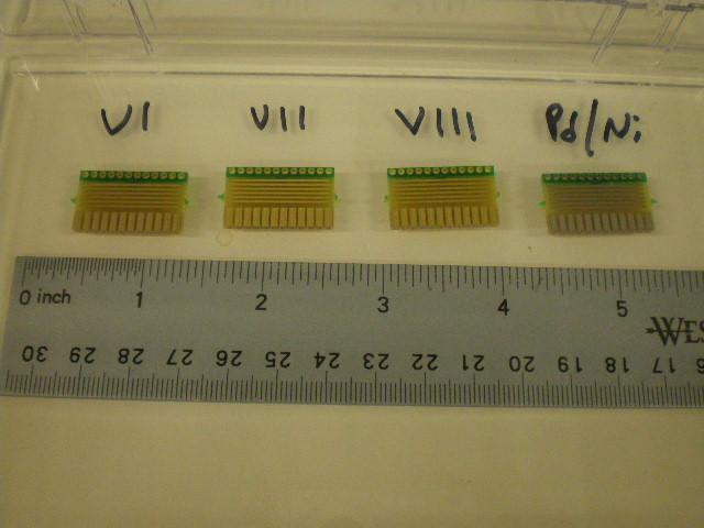
7
8 Round Robin Investigation The TVs are sent around again to the different testing sites that test for the desired attribute like soldering, contacting and wire bonding capabilities of the different finish thicknesses. The data is then collected sorted out and documented. At this point a new attempt at consensus is made and upon arrival the thickness specification is set.
9 The Document Draft After consensus is complete a draft is prepared. Peer Review 1. The draft is then posted for peer review. 2. Any IPC member can review the document and suggest technical or editorial changes 3. All comments are then reviewed and all issues are resolved before the final draft is issued. Publication At this time the IPC takes on the task of publishing the document in its final format.
10 The Committee Active since 2001 Co chaired by George Milad and Gerard O Brien IPC liaison is Tom Newton An Extensive Member List. OEMs Assembly Manufacturers Board manufacturers Suppliers Labs and Consultants
11 Member Companies 1 of 2 OEM and CM Lockheed Martin. Raytheon, Oracle, Adtran, Rockwell Collins, Heweltt Packard, Alcatel Lucent, Dell, St Jude Medical, Delphi, Schneider Electric, Continental Corporation, Panasonic, IBM, Northrop Grumman, BAE Systems, Honeywell, Boeing, Tyco Electronics, Peregrine Semiconductor, Space Systems /Loral, Amonix, Celestica, Winstron
12 Member Companies 2 of 2 Board Manufacturing Viasystems, TTM, I3, Molex, Superior Processing, Alternate Final Finishing, Suppliers Macdermid, OMG, Uyemura, Atotech, Cookson Electronics, MEC, ECI Technology, Kulick & Sofa, Metalor, Fischer Technology, Hesse Mechatronics, H Z O Labs and Consultants ST and S Group, Sandia labratories, DFR Solutions, TAS Consulting
13 Member Companies Operation o The committee operates thru one hour bi weekly conference calls. o All decisions are made in the concalls by those in attendance. o The call minutes are documented and circulated. Acknowledgement To date all committee activities have been voluntary and acknowledgement is in order for the members and equally important to their management that allow for the voluntary time invested by their employees.
14 IPC Specifications Plating Subcommittee 4 14 Since its inception the IPC Plating Sub committee 4 14 has issued the following: IPC 4552 ENIG Specification 2002 IPC 4552 ENIG Specification Amended 2012 IPC 4553 Immersion Silver specification 2005 IPC 4554 Immersion Tin Specification 2007 IPC 4553A Revised Immersion Silver 2009 IPC 4554 Amended Tin Specification 2011 IPC 4552 Amended ENIG Specification 2012 IPC 4556 ENEPIG Specification 2013
15 IPC 4552 ENIG Specification (2002) The ENIG IPC 4552 Specification was issued in 2002, No lead free (LF) solder in use. For thickness IPC 4552 stated : othe EN thickness shall be 3 to 6 µm [118.1 to µin] othe minimum IG thickness shall be 0.05 [1.97 µin] at four sigma (standard deviation) below the mean. The typical range is to µm [2.955 to µin].
16 IPC 4552 ENIG Specification (2002) To arrive at these numbers o The committee had conducted a series of test in a round robin (RR) study o The study included suppliers, PCB manufacturers, EMS providers and OEMs. o The data collected is summarized in the Appendix of the specification.
17 IPC 4552 ENIG Specification (2002) To arrive at these numbers o The committee had conducted a series of test in a round robin (RR) study o The study included suppliers, PCB manufacturers, EMS providers and OEMs. o The data collected is summarized in the Appendix of the specification.
18 IPC 4552 ENIG Specification (2002) To arrive at these numbers o The committee had conducted a series of test in a round robin (RR) study o The study included suppliers, PCB manufacturers, EMS providers and OEMs. o The data collected is summarized in the Appendix of the specification.
19 IPC 4552 ENIG Amended Spec (2012) The lower limit for Gold thickness was reduced from 0.05 µm to 0.04 µm (1.6 µin) With Restrictions: o Limited time from manufacturing to assembly o Demonstrate the consistency of the plating process. o Ability to measure low Gold thickness
20 IPC 4552 Rev A ENIG Specification The IPC 4552 A, ENIG Specification Revision is in progress. Expected completion 2015 The Purpose o To reduce the lower limit of Gold thickness and to set an upper limit. Under consideration 1.6 to 4.0 uins o Determine if the restrictions could be lifted. o This entails an extensive RR study o Testing to include LF solder and LF stressing conditions
21 IPC 4552 Rev A ENIG Specification The revision of IPC 4552 A would include the following Additional Documents: o Test Method (TM) for stripping Immersion gold during failure analysis o Test Method (TM) for determining the phos content of electroless nickel o Acceptability criteria for nickel corrosion (Black Pad). Include a CORROSION CHART

22 EXAMPLES OF CORROSION CHART Target condition no hyper corrosion defects or enhanced grain boundary definition Acceptable condition < 10 observations in the field of view


23 EXAMPLES OF CORROSION CHART Acceptable condition < 10 observations in the field of view Rejectable more than ten observations in the field of view

24 EXAMPLES OF CORROSION CHART Rejectable penetration to the copper surface Rejectable Evidence of contiguous corrosion with depth penetration > 10%
25 IPC 4553 Immersion Silver (2005) o In 2005 there were 2 distinct types of commercialized immersion silver with different thickness recommendations, referred to as Thin and Thick. o Each required its own thickness specification. o The initial 4553 specification stated the following for thickness of deposit
26 IPC 4553 Immersion Silver (2005) Two Thickness Specification: Thin Silver : 0.05µm(2µ ) minimum at 2σ from process mean as measured on a pad of area 2.25²µm (3600² mils). Typical value 0.07µm (3µ ) to 0.12µm (5µ ) Thick Silver: 0.12µm (5µ ) minimum at 4σ from process mean as measured on a pad of area 2.25²µm (3600² mils). Typical value of 0.2µm (8µ ) to 0.3µm (12µ ).
27 IPC 4553 A Immersion Silver (2009) A single Thickness Specified o 0.12 µm [5 µin] minimum to 0.4 µm [16 μin] maximum at ±4σ from process mean o As measured on a pad of area 2.25 mm² or 1.5 mm X 1.5 mm [approximately in² or in X in. o Typical value between 0.2 µm [8 µin] to 0.3 µm [12 µin]. oan Upper Limit was set.
28 IPC 4554 Immersion Tin (2007) For immersion tin the committee specified a lower limit for thickness. The relatively thick value of 1 micron was chosen to ensure that enough virgin tin would be available at the surface for soldering after storage. It is well understood that tin forms an intermetallic (IMC) layer with the underlying copper, and that this layer continues to grow in thickness over time.
29 IPC 4554 Immersion Tin (2007) The immersion tin thickness will be: 1.0 µm (40µ ) minimum at 4σ from process mean as measured on a pad of area 2.25²µm (3600² mils). Typical value of 1.15µm ( (46µ ) to 1.3µm (52µ ). The immersion tin Specification IPC 4554 was amended in The amendment addressed solderability testing and specified the allowed stress testing conditions for the deposit and the type of fluxes to be used for both tin/lead and LF testing.
30 IPC 4555 OSP Specification (No Date) After more than one year of struggling with specification IPC 4555; organic solderability preservative (OSP). Nothing was specified. There was no consensus arrived at. Mostly this was due to the wide assortment of organic products that were used for solderability preservation for the various application; each with its own thickness recommended values.
31 IPC 4556 ENEPIG Specification (2013) This is the last specification issued by the committee. The document produced is very comprehensive and includes a wealth of information from the RR studies that were conducted. The Appendix contains a documentation of these studies; each authored by the principle who conducted the testing. It also includes a section on the proper methods of equipment setup for a reliable measurement of very thin layers of metal deposits.
32 IPC 4556 ENEPIG Specification (2013) Appendices 1 thru9 1. Chemical Definitions and Process Sequence; Martin Bayes Dow Chemical Company 2. Round Robin Test Summary; George Milad Uyemura International Corporation 3. ENEPIG PWB Surface Finish XRF Round Robin Testing; Gerard O Brien S T and S Group. 4. Factors Affecting Measurement Accuracy of ENEPIG Coatings by XRF; Frank Ferrandino, Calmetrics Inc. 5. ENEPIG PWB Surface Finish Wetting Balance Testing; Gerard O Brien President S T and S Group. 6. Solder Spread Testing; Brian Madsen, Continental 7. ENEPIG PWB Surface Finish Shear Test Project; Dave Hillman,et al.rockwell Collins Inc. 8. Gold Wire Bonding; Stephen Meeks St Jude Medical 9. XRF Thickness Measurements of thin Au and Pd (ENEPIG): Recommendations for Instrumentation (Detectors) and their Limitations; Michael Haller Fischer Technology
33 IPC 4556 ENEPIG Specification (2013) The thickness specification for ENEPIG states Nickel: 3 to 6 µm [118.1 to µin] at ±4 sigma (standard deviations) from the mean. Palladium: 0.05 to 0.30 µm [2 to 12 µin] at ±4 sigma (standard deviations) from the mean. No upper limit. Gold: minimum µm [1.2 µin] at 4 sigma (standard deviations) below the mean. All measurements to be taken on a nominal pad size of 1.5 mm x 1.5 mm [0.060 in x in] or equivalent area.
34 IPC 4556 ENEPIG Specification Amended 2015 The thickness specification for ENEPIG states Nickel: 3 to 6 µm [118.1 to µin] at ±4 sigma (standard deviations) from the mean. Palladium: 0.05 to 0.30 µm [2 to 12 µin] at ±4 sigma (standard deviations) from the mean. No upper limit. Gold: minimum µm [1.2 µin] at 4 sigma (standard deviations) below the mean, maximum 0.07 µm [2.8 µin]. All measurements to be taken on a nominal pad size of 1.5 mm x 1.5 mm [0.060 in x in] or equivalent area.
35 IPC Specifications Plating Subcommittee 4 14 Committee conference calls are held every other Wednesday at 11:00 am EST. Call in Number is Pass Code is # Everyone is welcome to participate. A notification e mail is sent out before each conference call
36 IPC Plating Committee 4 14 Thank You George Milad gmilad@uyemura.com IMAPS New England Section 42nd Annual Symposium Technical Sessions May 5, 2015
STUDY OF IMMERSION GOLD PROCESSES THAT MAY BE USED FOR BOTH ENIG AND ENEPIG
 As originally published in the SMTA Proceedings STUDY OF IMMERSION GOLD PROCESSES THAT MAY BE USED FOR BOTH ENIG AND ENEPIG Don Gudeczauskas, Albin Gruenwald and George Milad UIC Technical Center Southington,
Optimizing Immersion Silver Chemistries For Copper
 Optimizing Immersion Silver Chemistries For Copper Ms Dagmara Charyk, Mr. Tom Tyson, Mr. Eric Stafstrom, Dr. Ron Morrissey, Technic Inc Cranston RI Abstract: Immersion silver chemistry has been promoted
Optimizing Immersion Silver Chemistries For Copper
 Optimizing Immersion Silver Chemistries For Copper Ms Dagmara Charyk, Mr. Tom Tyson, Mr. Eric Stafstrom, Dr. Ron Morrissey, Technic Inc Cranston RI Abstract: Immersion silver chemistry has been promoted
A STUDY OF THE ENEPIG IMC FOR EUTECTIC AND LF SOLDERS
 A STUDY OF THE ENEPIG IMC FOR EUTECTIC AND LF SOLDERS G.Milad, D.Gudeczauskas, G.Obrien, A.Gruenwald Uyemura International Corporation Southington, CT ABSTRACT: The solder joint formed on an ENEPIG surface
Effect of Process Variations on Solder Joint Reliability for Nickel-based Surface Finishes
 Effect of Process Variations on Solder Joint Reliability for Nickel-based Surface Finishes Hugh Roberts Atotech USA Inc., Rock Hill, SC, USA Sven Lamprecht, Gustavo Ramos and Christian Sebald Atotech Deutschland
EXTREME LONG TERM PRINTED CIRCUIT BOARD SURFACE FINISH SOLDERABILITY ASSESSMENT
 EXTREME LONG TERM PRINTED CIRCUIT BOARD SURFACE FINISH SOLDERABILITY ASSESSMENT Gerard O Brien, Solderability Testing and Solutions Inc., Richmond, KY Dave Hillman, Rockwell Collins, Cedar Rapids, IA INTRODUCTION
IMC Layers Formed with Various Combinations of Solders and Surface Finishes and Their Effect on Solder Joint Reliability
 IMC Layers Formed with Various Combinations of Solders and Surface Finishes and Their Effect on Solder Joint Reliability Per-Erik Tegehall, Swerea IVF 4 th Electronic Materials and Assembly Processes for
Technology HF-Printed Circuits Rev For latest information please visit
 Options and Characteristics Online calculation On explicit enquiry Quantity 1 piece up to 0,4m² total area from 1 piece to mass production Layer quantity 1 to 2 layers Up to 8 layers Material thickness
Press Fit Rework Project. Project Update HDPUG Meeting Düren, Germany 06/05/14
 Press Fit Rework Project Project Update HDPUG Meeting Düren, Germany 06/05/14 Background Since late 60 s or early 70 s First press fit was a square peg into a round hole using a fixed geometry solid pin
Practical guidelines for PWB Moisture Sensitivity, Packaging and Handling. Mumtaz Y. Bora Peregrine Semiconductor San Diego, CA, USA
 Practical guidelines for PWB Moisture Sensitivity, Packaging and Handling Mumtaz Y. Bora Peregrine Semiconductor San Diego, CA, USA Agenda and Overview Industry Standards for Moisture Sensitivity Packages
Welcome to the Real World of Lead Free Soldering
 Welcome to the Real World of Lead Free Soldering Metallic Resources, Inc. Howard Stevens Nimal Liyanage,, Ph.D Objective: to Provide Education Regarding the Effects of Various Lead Free Soldering Alloys
Palladium as diffusion barrier - a way to a multifunctional printed circuit board finish
 Palladium as diffusion barrier - a way to a multifunctional printed circuit board finish Dr. Norbert Sitte, Schwaebisch Gmuend, Umicore Galvanotechnik GmbH 1. Introduction Due to the continuing miniaturization
Control of Electroless Nickel Baths. Eugene Shalyt, Semyon Aleynik, Michael Pavlov, Peter Bratin, Chenting Lin ECI Technology, Totowa, New Jersey, USA
 Abstract Control of Electroless Nickel Baths Eugene Shalyt, Semyon Aleynik, Michael Pavlov, Peter Bratin, Chenting Lin ECI Technology, Totowa, New Jersey, USA This paper reports the authors work on developing
Evaluation of Pb-free BGA Solder Joint Reliability on Ni-based Surface Finishes using Alternative Shear and Pull Metrologies
 Evaluation of Pb-free BGA Solder Joint Reliability on Ni-based Surface Finishes using Alternative Shear and Pull Metrologies Kuldip Johal and Hugh Roberts Atotech USA Inc., Rock Hill, SC Sven Lamprecht,
Future Electronic Devices Technology in Cosmic Space and Lead-free Solder Joint Reliability
 The 22nd Microelectronics Work Future Electronic Devices Technology in Cosmic Space and Lead-free Solder Joint Reliability Key Points (1) High Speed Solder Ball Shear Test (2) Relationship between Surface
ELIMINATING FALSE POSITIVE ICT RESPONSE THROUGH THE USE OF ORGANIC-METAL FINAL FINISH
 ELIMINATING FALSE POSITIVE ICT RESPONSE THROUGH THE USE OF ORGANIC-METAL FINAL FINISH Rita Mohanty, John Fudala, Sathiya Narayana MacDermid Enthone, West Haven, CT ABSTRACT In-Circuit testing (ICT) is
PCB Production Process HOW TO PRODUCE A PRINTED CIRCUIT BOARD
 NCAB Group Seminars PCB Production Process HOW TO PRODUCE A PRINTED CIRCUIT BOARD NCAB GROUP PCB Production Process Introduction to Multilayer PCBs 2 Introduction to multilayer PCB s What is a multilayer
ATS Document Cover Page
 221-008 Item Rev Status: RELEASED printed 9/20/2017 2:27:42 PM by Les Deenin ATS: OPERATIN PROCEDURE ATS Document Cover Page Responsible Department: Supply Chain This copy is uncontrolled unless otherwise
Component Palladium Lead Finish - Specification Approved by Executive Board 1997-xx-xx August 22 Version
 Component Palladium Lead Finish - Specification Approved by Executive Board 1997-xx-xx August 22 Version Appendices 1. User Commitment Form 2. Supplier Compliance Form Table of contents 1. Background 2.
A NEW SURFACE FINISH FOR THE ELECTRONICS INDUSTRY Ernest Long PhD and Lenora Toscano MacDermid Waterbury, CT, USA
 A NEW SURFACE FINISH FOR THE ELECTRONICS INDUSTRY Ernest Long PhD and Lenora Toscano MacDermid Waterbury, CT, USA ABSTRACT The performance expectations for printed circuit board surface finishes are greater
The Elimination of Whiskers from Electroplated Tin
 The Elimination of Whiskers from Electroplated Tin by Masanobu Tsujimoto, Shigeo Hashimoto, Masayuki Kiso, Raihei Ikumoto,Toshikazu Kano and Genki Kanamori C. Uyemura & Co., Ltd. - Hirakata Japan & Don
THE EFFECTS OF PLATING MATERIALS, BOND PAD SIZE AND BOND PAD GEOMETRY ON SOLDER BALL SHEAR STRENGTH
 THE EFFECTS OF PLATING MATERIALS, BOND PAD SIZE AND BOND PAD GEOMETRY ON SOLDER BALL SHEAR STRENGTH Keith Rogers and Craig Hillman CALCE Electronic Products and Systems Center University of Maryland College
OMIKRON IMMERSION WHITE TIN. Florida CirTech, Inc. Greeley, Colorado USA. Revised 2/19/98
 OMIKRON TM IMMERSION WHITE TIN Revised 2/19/98 Florida CirTech, Inc. C T Florida CirTech, Inc. 1309 North 17th Avenue Greeley, CO 80631 Telephone: 1-800-686-6504 Fax: (970) 346-8331 Table of Contents Pages
Impacts of the bulk Phosphorous content of electroless Nickel layers to Solder Joint Integrity
 Impacts of the bulk Phosphorous content of electroless Nickel layers to Solder Joint Integrity Sven Lamprecht, Kuldip Johal, Dr. H.-J. Schreier, Hugh Roberts Atotech Deutschland GmbH Atotech USA, Berlin
INTRODUCTION OF A NEW PCB SURFACE FINISH FOR THE ELECTRONICS INDUSTRY
 INTRODUCTION OF A NEW PCB SURFACE FINISH FOR THE ELECTRONICS INDUSTRY Frank Ferdinandi Semblant Technologies Melbourne, United Kingdom ABSTRACT A new PCB surface finish has been developed that offers outstanding
SN100C Technical Guide
 SN100C Technical Guide INTRODUCTION SN100C is a lead-free tin/copper//germanium alloy. It has been in use since about the year 2000. Since then SN100C has become a world leading alloy in wave and selective
Electroless Nickel / Electroless Palladium / Immersion Gold Process For Multi-Purpose Assembly Technology
 ckel / Palladium / Gold Process For Multi-Purpose Assembly Technology Kuldip Johal and Hugh Roberts, Atotech USA Inc. Sven Lamprecht, Atotech Deutschland GmbH ABSTRACT As the second part to a paper presented
Metallization of MID Dec 2 010
 Metallization of MID Dec 2010 Agenda Introduction to Dow Electronic Materials MID Applications & Advantages Dow MID Metallization Processes Plating Equipment Summary Dow Business Structure Where Dow Electronic
Images of Failures in Microelectronics Packaging and Assembly
 Images of Failures in Microelectronics Packaging and Assembly Ed Hare, Ph.D./SEM Lab, Inc. IMAPS NW - Feb. 11th 2004 Redmond, WA http://www.semlab.com 1 What is this? http://www.semlab.com 2 Inner Layer
The hand soldering process can therefore be defined by the following steps ;
 Hand Soldering with Lead Free Alloys Introduction As companies start to implement lead free soldering processes, hand soldering and associated techniques have been identified as key functions in the manufacturing
Whisker free tin Jan Feb 2012-stripped:Metal Tech Speaking Template USE THIS.qxd 2/24/ :07 AM Page 1
 Whisker free tin Jan Feb 2012-stripped:Metal Tech Speaking Template USE THIS.qxd 2/24/2012 11:07 AM Page 1 BY GEORGE MILAD, NATIONAL ACCOUNTS MANAGER FOR TECHNOLOGY, UYEMURA USA, SOUTHINGTON, CONN. The
Thermal Fatigue Result for Low and No-Ag Alloys - Pb-Free Alloy Characterization Speaker: William Chao, Cisco Chair: Elizabeth Benedetto, HP
 Thermal Fatigue Result for Low and No-Ag Alloys - Pb-Free Alloy Characterization Speaker: William Chao, Cisco Chair: Elizabeth Benedetto, HP October 26, 2012 inemi Session, IMPACT Project Team Members
Investigation of the recommended immersion Tin thickness for Pbfree
 Investigation of the recommended immersion Tin thickness for Pbfree soldering Sven Lamprecht Atotech Deutschland GmbH Berlin Abstract First choices for Pb-free soldering are SnAgCu alloys, which are in
Bright Lights, Big Finish
 Reprinted From: Products Finishing Magazine Bright Lights, Big Finish for Electronics Plater Wisconsin maker of PCB for the LED industry adds new finishing line. BY TIM PENNINGTON EDITOR Business of late
Future Electronic Devices Technology in Cosmic Space and Electroless Ni/Pd/Au Plating for High Density Semiconductor Package Substrate
 JAXA 25 rd Microelectronics Workshop Future Electronic Devices Technology in Cosmic Space and Electroless Ni/Pd/Au Plating for High Density Semiconductor Package Substrate November 2, 2012 Yoshinori Ejiri
PCB Fabrication Specification
 Original Author: Steve Babiuch Process Owner: Steve Babiuch Page 2 of 8 1.0 Purpose This specification establishes the NEO Tech fabrication requirements for printed circuit boards. The order of precedence
White Paper Understanding the Risk of Gold Flash. By Randy Schueller and Craig Hillman
 White Paper Understanding the Risk of Gold Flash By Randy Schueller and Craig Hillman Introduction As the risk of depression fades and the electronics industry struggles to find its footing again, there
Manufacturing Capacity
 Capability List Manufacturing Capacity QTA & Prototype Layer : 1L ~32 L Impedance Board Ball Grid Array ( BGA ) Blind/ Buried Via Micro Via ( Laser Drilling) Flex /Rigid Flexible PCB Series Orders Layer
ViaSat, Inc. Quality PR Third Party Inspection Services, PWB Verification and DPA Samples Quality 1 of 12 Purpose and Scope
 ViaSat, Inc. Process Area: Document Number: Revision: Quality PR001362 001 Name of Document: Process Category: Page: Quality 1 of 12 1 Purpose and Scope The purpose of this procedure is to define the process
Overpad Metallizations and Probe Challenges
 Terence Q. Collier CVInc Overpad Metallizations and Probe Challenges June 6 to 9, 2010 San Diego, CA USA Why Packaging stuff at Probe Conference More and more wafers with ENIG finish Reliability data applicable
Technology Aluminium-IMS-PCBs Rev For latest information please visit
 Options and Characteristics Online calculation On explicit enquiry Quantity 1 piece up to 1,0² total area from 1 piece to mass production Layer quantity 1- and 2-layers up to 6 layers Material thickness
Axiom Electronics LLC
 1 of 8 1.0 PURPOSE and SCOPE This document defines Axiom s requirements for printed circuit board (PCB) fabrication, handling, and storage. Industry standards are referenced where appropriate. This document
Mitigation of Pure Tin Risk by Tin-Lead SMT Reflow
 Mitigation of Pure Tin Risk by Tin-Lead SMT Reflow Results of an Industry Round-Robin David Pinsky - Raytheon Integrated Defense Systems Tom Hester - Raytheon Space and Airborne Systems Dr. Anduin Touw
Reflow Profiling: Time a bove Liquidus
 Reflow Profiling: Time a bove Liquidus AIM/David Suraski Despite much research and discussion on the subject of reflow profiling, many questions and a good deal of confusion still exist. What is clear
A Marmon Engineered Wire & Cable Company
 A Marmon Engineered Wire & Cable Company MARMON Aerospace & Defense Tin Coated Copper Discussion MARMON Aerospace & Defense is committed to supplying the very best wire and cable for the aerospace industry.
Sample Preparation for Mitigating Tin Whiskers in alternative Lead-Free Alloys
 As originally published in the IPC APEX EXPO Conference Proceedings. Sample Preparation for Mitigating Tin Whiskers in alternative Lead-Free Alloys Mehran Maalekian Karl Seelig, V.P. Technology Timothy
POWERFUL PRINTED CIRCUIT BOARD MANUFACTURING SOLUTIONS
 POWERFUL PRINTED CIRCUIT BOARD MANUFACTURING SOLUTIONS Leading the PCB Industry in Quality & Innovation for over 25 Years Advanced Circuits, Inc. www.4pcb.com ABOUT ADVANCED CIRCUITS Founded in 1989 Third
Abstract. Key words. I. Introduction
 Increased High-Temperature Reliability and Package Hardening of Commercial Integrated Circuits (Through Die Extraction, Electroless Nickel/Gold Pad Reconditioning, and Ceramic Re-Assembly) Erick M. Spory
contaminated, or if the location of the assembly house is well above sea level.
 VAPOR PHASE REFLOW S EFFECT ON SOLDER PASTE RESIDUE SURFACE INSULATION RESISTANCE Karen Tellefsen. Mitch Holtzer, Corne Hoppenbrouwers Alpha Assembly Solutions South Plainfield, NJ, USA Roald Gontrum SmartTech
Mitigation of Pure Tin Risk by Tin-Lead SMT Reflow- Results of an Industry Round-Robin
 Mitigation of Pure Tin Risk by Tin-Lead SMT Reflow- Results of an Industry Round-Robin David Pinsky- Raytheon Integrated Defense Systems Tom Hester- Raytheon Space and Airborne Systems Dr. Anduin Touw-
IPC January Specification for Electroless Nickel/Electroless Palladium/ Immersion Gold (ENEPIG) Plating for Printed Circuit Boards
 Plating for Printed Circuit Boards") IPC-4556 2013 - January Specification for Electroless Nickel/Electroless Palladium/ Immersion Gold (ENEPIG) Plating for Printed Circuit Boards A standard developed by IPC Association Connecting Electronics
IPC-4556 2013 - January Specification for Electroless Nickel/Electroless Palladium/ Immersion Gold (ENEPIG) Plating for Printed Circuit Boards A standard developed by IPC Association Connecting Electronics
EFFECTIVENESS OF CONFORMAL COATINGS IN PREVENTING RESISTOR SILVER SULFIDE CORROSION
 As originally published in the SMTA Proceedings EFFECTIVENESS OF CONFORMAL COATINGS IN PREVENTING RESISTOR SILVER SULFIDE CORROSION Marie Cole, Jacob Porter, Jason Wertz, Marc Coq IBM Corporation Poughkeepsie,
Contamination on. Semiconductor Assembly: A Failure Analysis Perspective BY JONATHAN HARRIS, CMC LABORATORIES, INC.
 The Impact of Plated Layer Contamination on Semiconductor Assembly: A Failure Analysis Perspective BY JONATHAN HARRIS, CMC LABORATORIES, INC. In the world of both package and board level assembly, the
Effects of SAC Alloy Copper Dissolution Rates on PTH Processes: Cost and performance justify use of certain alternatives to SAC305/405
 Effects of SAC Alloy Copper Dissolution Rates on PTH Processes: Cost and performance justify use of certain alternatives to SAC305/405 1 Craig Hamilton, Polina Snugovsky (Celestica) & Matthew Kelly (IBM)
Lead-Free Connectors - An Overview
 Lead-Free Connectors - An Overview Pete Elmgren Molex Inc. 15 August 2003 Introduction For more than 50 years, lead-bearing solders have been used almost exclusively throughout the electronics industry
Soldering Immersion Tin
 Soldering Immersion Tin Rick Nichols and Sandra Heinemann Atotech Deutschland GmbH Berlin, Germany Abstract The stimulating impact of the automotive industry has sharpened focus on immersion tin (i-sn)
Quantification of Phosphorus Content in Electroless Nickel Immersion Gold Deposits
 Quantification of Phosphorus Content in Electroless Nickel Immersion Gold Deposits Joe CHONG*, Geoffrey TONG, Kenneth CHAN, Dennis CHAN & Dennis YEE Dow Electronic Materials Copper is well known as the
for High Reliable Gold Wire Bonding with Electronic Devices for Space Applications
 JAXA 23 rd Microelectronics Workshop Electroless ess Ni/Pd/ Plating for High Reliable Gold Wire Bonding with Electronic Devices for Space Applications (1) Plating Combinations and Reliability (2) Grain
NEWS FROM IPC. Conflict Minerals Legislation Moving Forward in the EU
 May 2015 NEWS FROM IPC Conflict Minerals Legislation Moving Forward in the EU by Fern Abrams Last week, I attended the ICGLR OECD UN Group of Experts Forum on Responsible Mineral Supply Chains. The meeting,
Bungard Surfaces Page 1 / 8
 Bungard Surfaces Page 1 / 8 This flyer is supposed to inform you about the different kinds of surfaces for your pcb. We hope to provide interesting information. If you encounter any questions or you need
Innovative MID Plating Solutions
 Innovative MID Plating Solutions High Reliability Wire Bond Technique for MIDs Jordan Kologe MacDermid Electronics Solutions jkologe@macdermid.com 1 MacDermid: Specialty Chemical Solutions Over 2000 Worldwide
Technical Note. Micron Wire-Bonding Techniques. Overview. Wire Bonding Basics. TN-29-24: Micron Wire-Bonding Techniques Overview
 Overview Technical Note Micron Wire-Bonding Techniques Overview For more than 30 years, the semiconductor industry has used aluminum (Al) bond pads with gold (Au) wire to connect internal die to external
NASA DOD PHASE 2: SAC305 AND SN100 COPPER DISSOLUTION TESTING
 NASA DOD PHASE 2: SAC305 AND SN100 COPPER DISSOLUTION TESTING ABSTRACT: Copper dissolution is a concern for products making the conversion to lead-free solder alloys. In these alloys, the more rapid reaction
Ultra Fine Pitch Bumping Using e-ni/au and Sn Lift-Off Processes
 Ultra Fine Pitch Bumping Using e-ni/au and Sn Lift-Off Processes Andrew Strandjord, Thorsten Teutsch, and Jing Li Pac Tech USA Packaging Technologies, Inc. Santa Clara, CA USA 95050 Thomas Oppert, and
IPC-6013A Amendment 2
 ASSOCIATION CONNECTING ELECTRONICS INDUSTRIES IPC-6013A Amendment 2 Qualification and Performance Specification for Flexible Printed Boards IPC-6013A Amendment 2 March 2006 A standard developed by IPC
THIN IMMERSION TIN USING ORGANIC METALS
 THIN IMMERSION TIN USING ORGANIC METALS Jim Kenny, Nils Arendt, Bernhard Wessling, and Karl Wengenroth Enthone Inc., A Business of Cookson Electronics West Haven, CT, USA ABSTRACT With the international
HBLED packaging is becoming one of the new, high
 Ag plating in HBLED packaging improves reflectivity and lowers costs JONATHAN HARRIS, President, CMC Laboratories, Inc., Tempe, AZ Various types of Ag plating technology along with the advantages and limitations
Cu Wire Bonding Survey Results. inemi Cu Wire Bonding Reliability Project Team Jan 30, 2011
 Cu Wire Bonding Survey Results inemi Cu Wire Bonding Reliability Project Team Jan 30, 2011 Outline About inemi Project Overview Survey Mechanism Survey Respondents Survey Results Technology Adoption Status
PBA Qualification Guideline
 EDM-Q-001 Rigid Printed Circuit Board Qualification Version 1.0 July 2017 Contact Geert Willems Phone: +32 16 288962 Mobile: +32 498 91 94 64 Geert.Willems@imec.be IMEC Kapeldreef 75 B3001 Heverlee Verantwoordelijke
Using Argon Plasma to Remove Fluorine, Organic and Metal Oxide Contamination for Improved Wire Bonding Performance
 Using Argon Plasma to Remove Fluorine, Organic and Metal Oxide Contamination for Improved Wire Bonding Performance Scott D. Szymanski March Plasma Systems Concord, California, U.S.A. sszymanski@marchplasma.com
Sample Preparation for Mitigating Tin Whiskers in alternative Lead-Free Alloys
 Sample Preparation for Mitigating Tin Whiskers in alternative Lead-Free Alloys Mehran Maalekian Karl Seelig, V.P. Technology Timothy O Neill, Technical Marketing Manager AIM Solder Cranston, RI Abstract
THIN MULTILAYER COATINGS FOR ADVANCED PROCESSING OF ELECTRONIC PACKAGES. I. V. Kadija J. A. Abys
 THIN MULTILAYER COATINGS FOR ADVANCED PROCESSING OF ELECTRONIC PACKAGES I. V. Kadija J. A. Abys AT&T Bell Laboratories 600 Mountain Avenue Murray Hill, NJ 07974 Abstract Current trends in electronic packaging
Reliability Assessment of No-clean and Water-soluble Solder Pastes Part II
 As originally published in the IPC APEX EXPO Conference Proceedings. Reliability Assessment of No-clean and Water-soluble Solder Pastes Part II Emmanuelle Guéné, Steven Teh INVENTEC Performance Chemicals
NEMI RoHS Transition Task Group Forum APEX 2004 February 26, Dave McCarron, Dell
 NEMI RoHS Transition Task Group Forum APEX 2004 February 26, 2004 Dave McCarron, Dell Agenda Introductions, Dave McCarron, Dell NEMI Overview, David Godlewski, NEMI Assembly Process Specifications, Frank
Hard Gold Plating vs Soft Gold Plating Which is Right for My Application? By: Matt Lindstedt, Advanced Plating Technologies
 Hard Gold Plating vs Soft Gold Plating Which is Right for My Application? By: Matt Lindstedt, Advanced Plating Technologies When specifying gold plating for an application, the question of hard gold plating
Characterization of 0.6mils Ag Alloy Wire in BGA Package
 Characterization of 0.6mils Ag Alloy Wire in BGA Package Toh Lee Chew, Alan Lumapar Visarra, *Fabien Quercia, *Eric Perriaud STMicroelectronics Muar, Tanjung Agas Industrial, P.O.Box 28, 84007, Muar, Johor
Question: Are RO4000 materials compatible with lead-free processes? Answer:
 Question: Are RO4 materials compatible with lead-free processes? Answer: RO4 cores and prepregs are among the most temperature stable products available. They easily meet or exceed all expectations for
T/C stress resistant high reliability solder alloy SB6NX / SB6N. Patented by Panasonic
 T/C stress resistant high reliability solder alloy X / Patented by Panasonic Sn 3.5Ag 0.5Bi 6.0In 0.8Cu Sn 3.5Ag 0.5Bi 6.0In X & solder alloy X alloy is Panasonic patented Conventional (Sn3.5Ag0.5Bi6In)
CANDOR Industries Inc. High Quality PCB Manufacturing Solutions
 CANDOR Industries Inc High Quality PCB Manufacturing Solutions 1 Our Mission Founded in 1999, Candor is an industry leader in High Technology Printed Circuit Board Fabrication Services. Quick turn services
New Pb-Free Solder Alloy for Demanding Applications. Presented by Karl Seelig, VP Technology, AIM
 New Pb-Free Solder Alloy for Demanding Applications Presented by Karl Seelig, VP Technology, AIM Why REL? The evolution and expansion of electronics into more harsh operating environments performing more
ISO 9001:2015 incorporating the Requirements of AS9100D Certificate 14035ASR006
 Coastline Metal Finishing is AS9100D Certified and NADCAP Accredited. ISO 9001:2015 incorporating the Requirements of AS9100D Certificate 14035ASR006 Nadcap Accredited AS7108 for Chemical Processing Thank
Lead Free Probe Series
 Lead Free Probe Series INTERCONNECT DEVICES, INC. Introducing the Probe Series for Lead Free Test Lead Free Simulation Test Against Matte Tin For 100k Cycles Probing boards manufactured with lead-free
Reliability Assessment of Immersion Silver Finished Circuit Board Assemblies Using Clay Tests
 Reliability Assessment of Immersion Silver Finished Circuit Board Assemblies Using Clay Tests Yilin Zhou Research Lab of Electric Contacts, Automation School Beijing University of Posts and Telecommunications
QUALITY MANUAL RED CHECK DENOTES THIS IS A CONTROLLED COPY. APPROVED BY: (President) APPROVED BY: (Production Manager) APPROVED BY: (Quality Manager)
 APPROVED BY: (Production Manager) APPROVED BY: (Quality Manager)") PNC, Inc. QUALITY MANUAL, Rev. 6 Date: 11-10-08 Page 1 of 17 QUALITY MANUAL RED CHECK DENOTES THIS IS A CONTROLLED COPY APPROVED BY: (President) APPROVED BY: (Production Manager) APPROVED BY: (Quality
PNC, Inc. QUALITY MANUAL, Rev. 6 Date: 11-10-08 Page 1 of 17 QUALITY MANUAL RED CHECK DENOTES THIS IS A CONTROLLED COPY APPROVED BY: (President) APPROVED BY: (Production Manager) APPROVED BY: (Quality
ROUND ROBIN TESTING OF CREEP CORROSION DEPENDENCE ON RELATIVE HUMIDITY
 ROUND ROBIN TESTING OF CREEP CORROSION DEPENDENCE ON RELATIVE HUMIDITY Prabjit Singh and Larry Palmer Corporation, Poughkeepsie, New York, USA pjsingh@us.ibm.com Haley Fu International Electronics Manufacturing
ALPHA EF product guide. Enabling Wave Soldering Flux Technology for Lead- Free Processing
 the product: Enabling Wave Soldering Flux Technology for Lead- Free Processing ALPHA EF-8000 product guide Contents TOPIC PAGE Introduction/Features-Benefits 3 Performance Summary 4 Hole Fill Performance
Welcome to SMTA Brazil Chapter Brook Sandy-Smith Dr. Ron Lasky Tim Jensen
 Welcome to SMTA Brazil Chapter 2013 Presented by Authors Ivan Castellanos Edward Briggs Brook Sandy-Smith Dr. Ron Lasky Tim Jensen Advantages / Concerns HP testing Mechanical properties New work Area ratio
LEAD FREE ALLOY DEVELOPMENT
 LEAD FREE ALLOY DEVELOPMENT Karl F. Seelig, VP of Technology AIM Cranston, RI. USA. kseelig@aimsolder.com Abstract. When lead-free solders were first introduced to the electronics industry in the early
Results of Mitigation Effectiveness Survey
 Results of Mitigation Effectiveness Survey &Plans for GEIA-STD-0005-2 Revision Anduin E. Touw Task Team Lead for PERM GEIA-STD-0005-2 Associate Technical Fellow, The Boeing Company anduin.e.touw@boeing.com
Int. CI.*: B 32 B 15/01 B 32 B 15/18, B 32 B 3/00 C 25 D 5/14, H 01 L 21/48 H 01 L 23/02. Morristown, NJ 07960IUS)
") Europaisches Patentamt European Patent Office Office europeen des brevets Publication number: 0 175 901 A1 EUROPEAN PATENT APPLICATION Application number: 85110121.2 Date of filing: 13.08.85 Int. CI.*:
Europaisches Patentamt European Patent Office Office europeen des brevets Publication number: 0 175 901 A1 EUROPEAN PATENT APPLICATION Application number: 85110121.2 Date of filing: 13.08.85 Int. CI.*:
ISO 9001:2015 incorporating the Requirements of AS9100D Certificate 14035ASR006
 Coastline Metal Finishing is AS9100D Certified and NADCAP Accredited. ISO 9001:2015 incorporating the Requirements of AS9100D Certificate 14035ASR006 Nadcap Accredited AS7108 for Chemical Processing Thank
MATERIAL NEEDS AND RELIABILITY CHALLENGES IN AUTOMOTIVE PACKAGING UNDER HARSH CONDITIONS
 MATERIAL NEEDS AND RELIABILITY CHALLENGES IN AUTOMOTIVE PACKAGING UNDER HARSH CONDITIONS Varughese Mathew NXP Semiconductors 6501 William Cannon Drive, Austin TX, USA Automotive Innovation Driven by Electronics
VERIFYING MICROVOID ELIMINATION AND PREVENTION VIA AN OPTIMIZED IMMERSION SILVER PROCESS
 VERIFYING MICROVOID ELIMINATION AND PREVENTION VIA AN OPTIMIZED IMMERSION SILVER PROCESS John Swanson and Donald Cullen MacDermid, Inc. Waterbury, CT USA Abstract The Pb-free transition in the electronics
Effects of Solder Reflow Conditions on the Assembly of Electronics Packaging and Printed Circuit Boards
 Effects of Solder Reflow Conditions on the Assembly of Electronics Packaging and Printed Circuit Boards Gregory K. Arslanian, Minfa Lin, Amy Wressell, Tom Mebrahtu, Victor Wang Air Products and Chemicals
Advances in Printing nano Cu and Using Existing Cu Based Manufacturing Processes. Michael J. Carmody Chief Scientist, Intrinsiq Materials
 Advances in Printing nano Cu and Using Existing Cu Based Manufacturing Processes Michael J. Carmody Chief Scientist, Intrinsiq Materials Why Use Copper? Lower Cost than Silver. Print on Numerous Substrates.
Biggest Pb-Free Challenges
 Biggest Pb-Free Challenges Randy Schueller, Ph.D. rschueller@dfrsolutions.com November 7, 2012 1 What are the primary Pb-Free Concerns and how are they being addressed? o Tin Whisker Mitigation o PCB Surface
Active Projects and Research Review
 Active Projects and Research Review Denis Barbini, Ph.D., Vitronics Soltec Productronica Munich, Germany November 17, 2005 1 Overview 2 Pb-Free BGAs in SnPb Process Study Chair: Robert Kinyanjui, Sanmina-SCI
Creep corrosion of electronic assemblies in harsh environments
 Creep corrosion of electronic assemblies in harsh environments Petri Savolainen* and Randy Schueller DfR Solutions 5110 Roanoke Place, Suite 101, College Park, MD 20740 * Business Center Länsikeskus, Pihatörmä