for High Reliable Gold Wire Bonding with Electronic Devices for Space Applications
|
|
|
- Lillian Phelps
- 5 years ago
- Views:
Transcription
1 JAXA 23 rd Microelectronics Workshop Electroless ess Ni/Pd/ Plating for High Reliable Gold Wire Bonding with Electronic Devices for Space Applications (1) Plating Combinations and Reliability (2) Grain Size and Crystal Growth (3) Diffusion of Underplated Metal onto surface (4) Wire Bonding Reliability Ranking of Plating Yukihisa Hiroyama Hitachi Chemical Co., Ltd.
2 1 Structure of BGA Assembly Gold Wire Semiconductor Chip Die Bonding Material Wire Bonding Solder Joint Package Substrate t Printed Circuit Board Molding Material Solder Ball


3 2 Wire Bonding Copper Line Aluminum Electrode LSI Gold Wire Resist Die Bonding Material Package Substrate Gold Plated Terminal


4 3 Solder Ball Joint Copper Pad Package Substrate Resist Solder Ball Solder Ball Gold Plated Terminal
5 4 Characterization of Gold Plating Item E lytic Ni/ (5/0.5µm) 5µm) E less Ni/ (ENIGEG) (5/0.5µm) 5µm) E less Ni/Pd/ (ENEPIGEG) (5/0.5/0.5µm) 5µm) Wire Bondability OK OK OK Wire Bondability after Aging* Wire Bondability after Aging* and Plasma** OK NG OK OK OK OK Solder Joint Reliability OK NG OK * Aging : 150ºC, 50 hours ** Plasma : O 2 plasma
6 5 Gold Plating Combination i with E less and E lytic Processes Gold Plating Process ENEPIGEG (Ni/Pd/) ENEPIG (Ni/Pd/IG) ENIGEG (Ni/) Ni(SBWatt)/E lytic Ni(BWatt)/E lytic Ni(BSulf)/E lytic Ni(SBWatt)/IGEG EN/E lytic Cu/E lytic Thickness (µm) 5/0.5/0.5 5/0.5/0.05 5/0.5 5/0.5 5/0.5 5/0.5 5/0.55 5/
7 6 Wire Bonding Reliability of Gold Plating Combinations As Gold Plating HeatTreatment 8 (150 o C, 3h) Pulll Strength (gf) 0 ENEPIGEG (Ni/Pd/) ENEPIG (Ni/ Pd/IG) ENIGEG (N Ni/) Ni(SBWatt) /E lytic Ni(BWatt) /E lytic Ni(BSulf.) /E lytic Ni(SBWatt) /IGEGG EN/E'lytic Cu/E'lytic
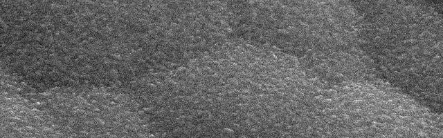


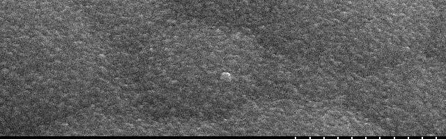

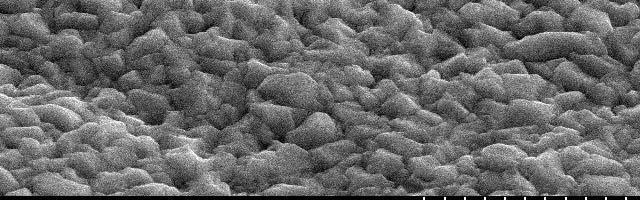
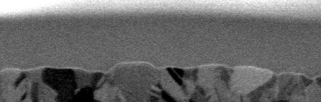
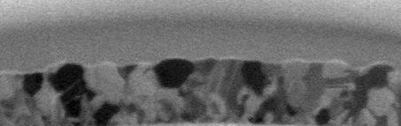

8 7 Surface Morphology and FIB/SIM Cross Section ENEPIGEG (Ni/Pd/) ENEPIG (Ni/Pd/IG) ENIGEG (Ni/) FIB/SIM Cro oss Sect tion Sur rface Morph hology Pd Ni 1 µm Pd Ni 1 µm Ni 1 µm
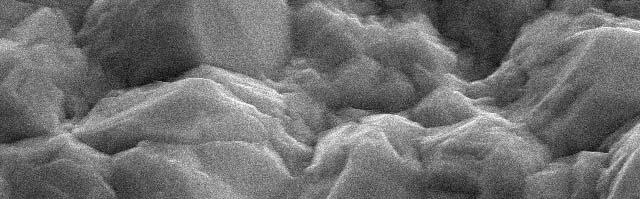
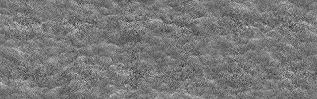
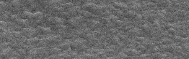
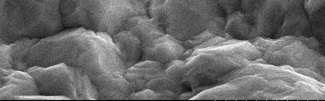
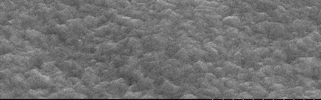


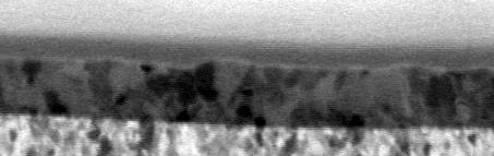


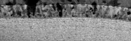
9 8 Surface Morphology and FIB/SIM Cross Section Ni(SBWatt)/ Ni(BWatt)/ Ni(BSulf.)/ Sur rface Morph hology FIB/SIM Cro oss Sect tion Ni 1 µm Ni 1 µm Ni 1 µ m
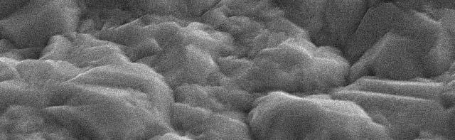

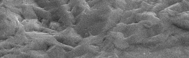
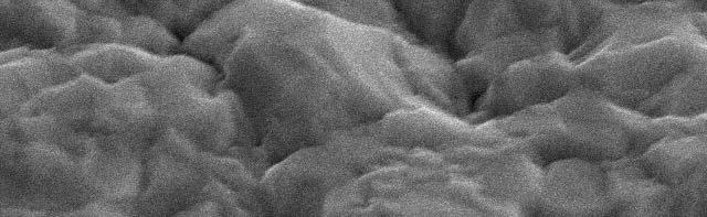
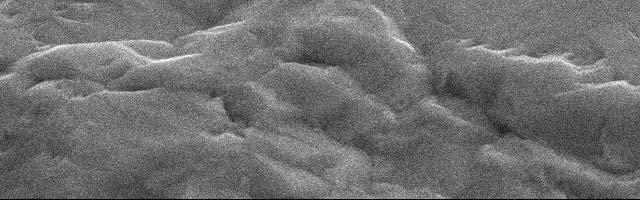


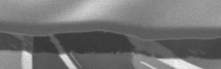
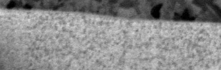


10 9 Surface Morphology and FIB/SIM Cross Section Ni(SBWatt)/IGEG EN/E lytic Cu/E lytic Sur rface Morph hology FIB/SIM Cro oss Sect tion Ni 1 µm Ni 1 µm Cu 1 µm

/E lytic")


/IGEG EN/E")


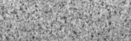
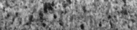
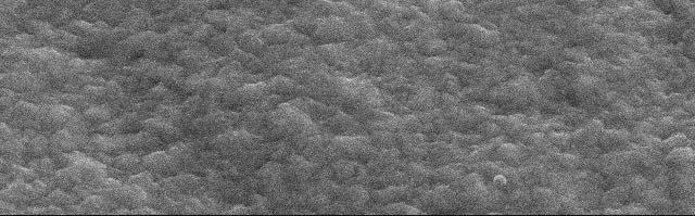
11 10 EBSP Mapping of Gold ENEPIGEG (Ni/Pd/) ENIGEG (Ni/) Ni(SBWatt)/E lytic Ni(BWatt)/E lytic 0.18 m m mm m m2 Ni(BSulf.)/E lytic Ni(SBWatt)/IGEG EN/E lytic Cu/E lytic m m m 0.03 m m : Average crosssectional area of gold grain EBSP: Electron Back Scattering Pattern


12 11 EBSP Mapping Ni(SBWatt)/IGEG Ni Ni Ni Cu Cu Cu 1 m All Ni Cu EDX E lytic Ni(SBWatt)/IGEG Energy Dispersion EBSP: Electron Back Scattering Profile Xray Spectrometry
 Electroless")


13 12 EBSP Mapping ENEPIGEG (Ni/Pd/) Electroless Ni/Electroless Pd/ Immersion /Electroless Pd Pd Pd 0.5 m All Pd EDX ENEPIGEG EBSP: Electron Back Scattering Profile Energy Dispersion Xray Spectrometry


14 13 EBSP Mapping Cu/E lytic Copper/Electrolytic Cu Cu All Cu Cu/E lytic EBSP: Electron Back Scattering Profile Cu 0.5 m EDX Energy Dispersion Xray Spectrometry
15 14 Thermal Diffusion Behavior of Underplated Metal By XPS Analysis (Xray Photoelectron Spectrometry) Gold Plating 3 hours 25 hours 50 hours Process Ni Cu Pd Ni Cu Pd Ni Cu Pd ENEPIGEG (Ni/Pd/) ENEPIG (Ni/Pd/IG) ENIGEG (Ni/) Ni(SBWatt)/ Ni(BWatt)/ Ni(BSulf)/ Ni(SBWatt)/IGEG EN/E lytic Cu/E lytic Atomic% Heat Treatment: 150ºC
16 15 Nickel Distribution over Gold Plating Surface By AES Analysis (ger Electron Spectrometry) ENIGEG (Electroless Ni/) : 5µm/0.5µm Heat Treatment: 150ºC, 50h Ni A u
17 16 Grain Boundary Diffusion i and Bulk Diffusion (Interdiffusion) Contamination on Gold Surface Grain Boundary Bulk Diffusion (Interdiffusion) Gold Under Plated Metal Gold Grain Grain Boundary Diffusion Under Plated Metal Grain
 IGEG IGEG EP EP EN FIB/SIM Analytical Result EN Grain Boundary")
18 17 Model of Grain Structure and Diffusion on ENEPIGEG ENEPIGEG (Electroless Ni/Pd/) IGEG IGEG EP EP EN FIB/SIM Analytical Result EN Grain Boundary Diffusion
19 18 Model of Grain Structure and Diffusion on Ni(SBWatt)/ E lytic NiO E lytic or IGEG Ni(SBWatt) IGEG (E less ) Ni(SBWatt) Ni(SBWatt) FIB/SIM Analytical Result Grain Boundary Diffusion
20 19 Model of Grain Structure and Diffusion on BNi/ and EN/ E less Ni/ IGEG EN NiO IGEG or E lytic E lytic EN E lytic Ni(BWatt) FIB/SIM Analytical Result Bright Ni and EN E lytic Bright Ni Plating (1) Bright Watt (2) Bright Sulfamate Grain Boundary Diffusion
21 20 Model of Grain Structure and Diffusion on ENEPIG ENEPIG (Electroless Ni/Pd/IG) Pd Organic Contamination IG IG EP EP EN FIB/SIM Analytical Result EN Grain Boundary Diffusion


")
22 21 Model of Grain Structure and Diffusion on Cu/E lytic CuO (Grain boundary) CuO (Bulk) E lytic E lytic Cu FIB/SIM Analytical Result Cu Interdiffusion (Bulk Diffusion) Grain Boundary Diffusion
23 22 Estimated Ranking of Wire Bonding Reliability Good ENEPIGEG, Ni(SBWatt)/IGEG and Ni(SBWatt)/E lytic Wire Bondin ng Relia ability ENEPIG, Ni(BWatt)/E lytic And Ni(BSulf.)/E lytic lytic ENIGEG, EN/E lytic Poor Cu/E lytic
24 23 Summary (1) The reliability of ENEPIGEG (E less Ni/Pd/) and E lytic Ni (SBWatt)/IGEG was equivalent to thatt of E lytic Ni (SB Watt)/E lytic after the heat treatment. (2) The reliability dependedd d on the diffusioni behavior of the underplated metals and the grain size of the gold deposit. (3) The grain size of plating coordinated with the grain size of the underplated d metals as the epitaxial crystal growth.
Future Electronic Devices Technology in Cosmic Space and Electroless Ni/Pd/Au Plating for High Density Semiconductor Package Substrate
 JAXA 25 rd Microelectronics Workshop Future Electronic Devices Technology in Cosmic Space and Electroless Ni/Pd/Au Plating for High Density Semiconductor Package Substrate November 2, 2012 Yoshinori Ejiri
Future Electronic Devices Technology in Cosmic Space and Lead-free Solder Joint Reliability
 The 22nd Microelectronics Work Future Electronic Devices Technology in Cosmic Space and Lead-free Solder Joint Reliability Key Points (1) High Speed Solder Ball Shear Test (2) Relationship between Surface
EFFECT OF THE MICROSTRUCTURE OF Ni/Au METALLIZATION ON BONDABILITY OF FR-4 SUBSTRATE
 EFFECT OF THE MICROSTRUCTURE OF Ni/Au METALLIZATION ON BONDABILITY OF FR-4 SUBSTRATE Zonghe Lai and Johan Liu The Swedish Institute of Production Engineering Research (IVF) S-431 53 Mölndal, Sweden ABSTRACT
Palladium as diffusion barrier - a way to a multifunctional printed circuit board finish
 Palladium as diffusion barrier - a way to a multifunctional printed circuit board finish Dr. Norbert Sitte, Schwaebisch Gmuend, Umicore Galvanotechnik GmbH 1. Introduction Due to the continuing miniaturization
Effect of Process Variations on Solder Joint Reliability for Nickel-based Surface Finishes
 Effect of Process Variations on Solder Joint Reliability for Nickel-based Surface Finishes Hugh Roberts Atotech USA Inc., Rock Hill, SC, USA Sven Lamprecht, Gustavo Ramos and Christian Sebald Atotech Deutschland
Overpad Metallizations and Probe Challenges
 Terence Q. Collier CVInc Overpad Metallizations and Probe Challenges June 6 to 9, 2010 San Diego, CA USA Why Packaging stuff at Probe Conference More and more wafers with ENIG finish Reliability data applicable
Comparative Study of NiNiP Leadframes from Different Processes
 Comparative Study of NiNiP Leadframes from Different Processes Wu-Hu Li *1, Jeffrey Khai Huat Low 1, Harry Sax 2, Raymond Solis Cabral 1, Esperidion De Castro Salazar 1, Pauline Min Wee Low 1 1 Infineon
IMC Layers Formed with Various Combinations of Solders and Surface Finishes and Their Effect on Solder Joint Reliability
 IMC Layers Formed with Various Combinations of Solders and Surface Finishes and Their Effect on Solder Joint Reliability Per-Erik Tegehall, Swerea IVF 4 th Electronic Materials and Assembly Processes for
A STUDY OF THE ENEPIG IMC FOR EUTECTIC AND LF SOLDERS
 A STUDY OF THE ENEPIG IMC FOR EUTECTIC AND LF SOLDERS G.Milad, D.Gudeczauskas, G.Obrien, A.Gruenwald Uyemura International Corporation Southington, CT ABSTRACT: The solder joint formed on an ENEPIG surface
High-Temperature-Resistant Interconnections Formed by Using Nickel Micro-plating and Ni Nano-particles for Power Devices
 Kato et al.: High-Temperature-Resistant Interconnections (1/6) [Technical Paper] High-Temperature-Resistant Interconnections Formed by Using Nickel Micro-plating and Ni Nano-particles for Power Devices
Advanced Analytical Techniques for Semiconductor Assembly Materials and Processes. Jason Chou and Sze Pei Lim Indium Corporation
 Advanced Analytical Techniques for Semiconductor Assembly Materials and Processes Jason Chou and Sze Pei Lim Indium Corporation Agenda Company introduction Semiconductor assembly roadmap challenges Fine
Technology Drivers for Plasma Prior to Wire Bonding
 Technology Drivers for Plasma Prior to Wire Bonding James D. Getty Nordson MARCH Concord, CA, USA info@nordsonmarch.com Technology Drivers for Plasma Prior to Wire Bonding Page 1 ABSTRACT Advanced packaging
Chapter 4 Fabrication Process of Silicon Carrier and. Gold-Gold Thermocompression Bonding
 Chapter 4 Fabrication Process of Silicon Carrier and Gold-Gold Thermocompression Bonding 4.1 Introduction As mentioned in chapter 2, the MEMs carrier is designed to integrate the micro-machined inductor
Bonding Pad Fabrication for Printed Electronics Using Silver Nanoparticles
 Nakatani et al.: Bonding Pad Fabrication for Printed Electronics (1/5) [Technical Paper] Bonding Pad Fabrication for Printed Electronics Using Silver Nanoparticles Makoto Nakatani, Haruyuki Nakajo, Hiroshi
Metallization of MID Dec 2 010
 Metallization of MID Dec 2010 Agenda Introduction to Dow Electronic Materials MID Applications & Advantages Dow MID Metallization Processes Plating Equipment Summary Dow Business Structure Where Dow Electronic
Three-Dimensional Molded Interconnect Devices (3D-MID)
") Jörg Frank Three-Dimensional Molded Interconnect Devices (3D-MID) Materials, Manufacturing, Assembly and Applica ons for Injec on Molded Circuit Carriers Sample Pages ISBN 978-1-56990-551-7 HANSER Hanser
Jörg Frank Three-Dimensional Molded Interconnect Devices (3D-MID) Materials, Manufacturing, Assembly and Applica ons for Injec on Molded Circuit Carriers Sample Pages ISBN 978-1-56990-551-7 HANSER Hanser
Contamination on. Semiconductor Assembly: A Failure Analysis Perspective BY JONATHAN HARRIS, CMC LABORATORIES, INC.
 The Impact of Plated Layer Contamination on Semiconductor Assembly: A Failure Analysis Perspective BY JONATHAN HARRIS, CMC LABORATORIES, INC. In the world of both package and board level assembly, the
Electroless Nickel / Electroless Palladium / Immersion Gold Process For Multi-Purpose Assembly Technology
 ckel / Palladium / Gold Process For Multi-Purpose Assembly Technology Kuldip Johal and Hugh Roberts, Atotech USA Inc. Sven Lamprecht, Atotech Deutschland GmbH ABSTRACT As the second part to a paper presented
Technical Note. Micron Wire-Bonding Techniques. Overview. Wire Bonding Basics. TN-29-24: Micron Wire-Bonding Techniques Overview
 Overview Technical Note Micron Wire-Bonding Techniques Overview For more than 30 years, the semiconductor industry has used aluminum (Al) bond pads with gold (Au) wire to connect internal die to external
Thermosonic Gold Ball Bonding to Immersion Gold/Electroless Nickel Plating Finishes on Laminate MCM Substrates. Abstract.
 Thermosonic Gold Ball Bonding to Immersion Gold/Electroless Nickel Plating Finishes on Laminate MCM Substrates Chris Dunn, R. Wayne Johnson Mike Bozack Auburn University 200 Broun Hall, EE Dept. Auburn,
STUDY OF IMMERSION GOLD PROCESSES THAT MAY BE USED FOR BOTH ENIG AND ENEPIG
 As originally published in the SMTA Proceedings STUDY OF IMMERSION GOLD PROCESSES THAT MAY BE USED FOR BOTH ENIG AND ENEPIG Don Gudeczauskas, Albin Gruenwald and George Milad UIC Technical Center Southington,
THIN MULTILAYER COATINGS FOR ADVANCED PROCESSING OF ELECTRONIC PACKAGES. I. V. Kadija J. A. Abys
 THIN MULTILAYER COATINGS FOR ADVANCED PROCESSING OF ELECTRONIC PACKAGES I. V. Kadija J. A. Abys AT&T Bell Laboratories 600 Mountain Avenue Murray Hill, NJ 07974 Abstract Current trends in electronic packaging
Using Argon Plasma to Remove Fluorine, Organic and Metal Oxide Contamination for Improved Wire Bonding Performance
 Using Argon Plasma to Remove Fluorine, Organic and Metal Oxide Contamination for Improved Wire Bonding Performance Scott D. Szymanski March Plasma Systems Concord, California, U.S.A. sszymanski@marchplasma.com
Images of Failures in Microelectronics Packaging and Assembly
 Images of Failures in Microelectronics Packaging and Assembly Ed Hare, Ph.D./SEM Lab, Inc. IMAPS NW - Feb. 11th 2004 Redmond, WA http://www.semlab.com 1 What is this? http://www.semlab.com 2 Inner Layer
General Introduction to Microstructure Technology p. 1 What is Microstructure Technology? p. 1 From Microstructure Technology to Microsystems
 General Introduction to Microstructure Technology p. 1 What is Microstructure Technology? p. 1 From Microstructure Technology to Microsystems Technology p. 9 The Parallels to Microelectronics p. 15 The
Innovative MID Plating Solutions
 Innovative MID Plating Solutions High Reliability Wire Bond Technique for MIDs Jordan Kologe MacDermid Electronics Solutions jkologe@macdermid.com 1 MacDermid: Specialty Chemical Solutions Over 2000 Worldwide
Silicon Wafer Processing PAKAGING AND TEST
 Silicon Wafer Processing PAKAGING AND TEST Parametrical test using test structures regularly distributed in the wafer Wafer die test marking defective dies dies separation die fixing (not marked as defective)
Lead-Free Solder Bump Technologies for Flip-Chip Packaging Applications
 Lead-Free Solder Bump Technologies for Flip-Chip Packaging Applications Zaheed S. Karim 1 and Jim Martin 2 1 Advanced Interconnect Technology Ltd. 1901 Sunley Centre, 9 Wing Yin Street, Tsuen Wan, Hong
Project Proposal. Cu Wire Bonding Reliability Phase 3 Planning Webinar. Peng Su June 6, 2014
 Project Proposal Cu Wire Bonding Reliability Phase 3 Planning Webinar Peng Su June 6, 2014 Problem Statement Background Work of the inemi Cu wire reliability project identified that bonding quality and
Ultra Fine Pitch Bumping Using e-ni/au and Sn Lift-Off Processes
 Ultra Fine Pitch Bumping Using e-ni/au and Sn Lift-Off Processes Andrew Strandjord, Thorsten Teutsch, and Jing Li Pac Tech USA Packaging Technologies, Inc. Santa Clara, CA USA 95050 Thomas Oppert, and
HBLED packaging is becoming one of the new, high
 Ag plating in HBLED packaging improves reflectivity and lowers costs JONATHAN HARRIS, President, CMC Laboratories, Inc., Tempe, AZ Various types of Ag plating technology along with the advantages and limitations
Arch. Metall. Mater. 62 (2017), 2B,
, 2B,") Arch. Metall. Mater. 62 (2017), 2B, 1225-1229 DOI: 10.1515/amm-2017-0182 S.S. KIM*, I. SON* #, K.T. KIM** EFFECT OF ELECTROLESS Ni P PLATING ON THE BONDING STRENGTH OF Bi Te-BASED THERMOELECTRIC MODULES
Arch. Metall. Mater. 62 (2017), 2B, 1225-1229 DOI: 10.1515/amm-2017-0182 S.S. KIM*, I. SON* #, K.T. KIM** EFFECT OF ELECTROLESS Ni P PLATING ON THE BONDING STRENGTH OF Bi Te-BASED THERMOELECTRIC MODULES
Bright Lights, Big Finish
 Reprinted From: Products Finishing Magazine Bright Lights, Big Finish for Electronics Plater Wisconsin maker of PCB for the LED industry adds new finishing line. BY TIM PENNINGTON EDITOR Business of late
Microelectronics. Integrated circuits. Introduction to the IC technology M.Rencz 11 September, Expected decrease in line width
 Microelectronics Introduction to the IC technology M.Rencz 11 September, 2002 9/16/02 1/37 Integrated circuits Development is controlled by the roadmaps. Self-fulfilling predictions for the tendencies
Novel Technique for Flip Chip Packaging of High power Si, SiC and GaN Devices. Nahum Rapoport, Remtec, Inc.
 Novel Technique for Flip Chip Packaging of High power Si, SiC and GaN Devices Nahum Rapoport, Remtec, Inc. 1 Background Electronic Products Designers: under pressure to decrease cost and size Semiconductor
Advances in Printing nano Cu and Using Existing Cu Based Manufacturing Processes. Michael J. Carmody Chief Scientist, Intrinsiq Materials
 Advances in Printing nano Cu and Using Existing Cu Based Manufacturing Processes Michael J. Carmody Chief Scientist, Intrinsiq Materials Why Use Copper? Lower Cost than Silver. Print on Numerous Substrates.
Evaluation of Pb-free BGA Solder Joint Reliability on Ni-based Surface Finishes using Alternative Shear and Pull Metrologies
 Evaluation of Pb-free BGA Solder Joint Reliability on Ni-based Surface Finishes using Alternative Shear and Pull Metrologies Kuldip Johal and Hugh Roberts Atotech USA Inc., Rock Hill, SC Sven Lamprecht,
EFFECTS OF THERMAL AGING ON INTERMETALLIC COMPOUNDS AND VOIDS FORMATION IN AuAl WIRE BONDING. A. Jalar, M. F. Rosle and M. A. A.
 EFFECTS OF THERMAL AGING ON INTERMETALLIC COMPOUNDS AND VOIDS FORMATION IN AuAl WIRE BONDING A. Jalar, M. F. Rosle and M. A. A. Hamid School of Applied Physics, Faculty of Science and Technology, Universiti
*EP A2* EP A2 (19) (11) EP A2 (12) EUROPEAN PATENT APPLICATION. (43) Date of publication: Bulletin 2005/08
 (11) EP A2 (12) EUROPEAN PATENT APPLICATION. (43) Date of publication: Bulletin 2005/08") (19) Europäisches Patentamt European Patent Office Office européen des brevets *EP00891A2* (11) EP 1 08 91 A2 (12) EUROPEAN PATENT APPLICATION (43) Date of publication: 23.02.0 Bulletin 0/08 (1) Int Cl.
(19) Europäisches Patentamt European Patent Office Office européen des brevets *EP00891A2* (11) EP 1 08 91 A2 (12) EUROPEAN PATENT APPLICATION (43) Date of publication: 23.02.0 Bulletin 0/08 (1) Int Cl.
Growth Kinetics of Reaction Layers in Flip Chip Joints with Cu-cored Lead-free Solder Balls
 Materials Transactions, Vol. 5, No. 3 () pp. 75 to 75 Special Issue on Lead-Free Soldering in Electronics # The Japan Institute of Metals Growth Kinetics of Reaction Layers in Flip Chip Joints with Cu-cored
1. Aluminum alloys for direct contacts. 1.1 Advantages of aluminum alloys for direct contacts
 Direct contacts between aluminum alloys and thin film transistors (TFTs) contact layers were studied. An Al-Ni alloy was found to be contacted directly with an indium tin oxide (ITO) layer successfully
How Bad's the Damage?
 How Bad's the Damage? Evaluating Probe Damage On Aluminum, Solder, Gold, UBM, and Copper Pads. Ken Smith Vice President of Technology Development Pyramid Probe Division, Cascade Microtech Goal of Presentation
Advances in Printing nano Cu and Using Existing Cu Based Manufacturing Processes. Michael J. Carmody Chief Scientist, Intrinsiq Materials
 Advances in Printing nano Cu and Using Existing Cu Based Manufacturing Processes Michael J. Carmody Chief Scientist, Intrinsiq Materials Why Use Copper? Lower Cost than Silver. Print on Numerous Substrates.
Australian Journal of Basic and Applied Sciences. Pb-Free Solder Ball Robustness Comparison under AC and TC Reliability Test
 AENSI Journals Australian Journal of Basic and Applied Sciences ISSN:1991-8178 Journal home page: www.ajbasweb.com Pb-Free Solder Ball Robustness Comparison under AC and TC Reliability Test 1,2 Tan Cai
Optimizing Immersion Silver Chemistries For Copper
 Optimizing Immersion Silver Chemistries For Copper Ms Dagmara Charyk, Mr. Tom Tyson, Mr. Eric Stafstrom, Dr. Ron Morrissey, Technic Inc Cranston RI Abstract: Immersion silver chemistry has been promoted
Copper Interconnect Technology
 Tapan Gupta Copper Interconnect Technology i Springer Contents 1 Introduction 1 1.1 Trends and Challenges 2 1.2 Physical Limits and Search for New Materials 5 1.3 Challenges 6 1.4 Choice of Materials 7
Chapter 3 Silicon Device Fabrication Technology
 Chapter 3 Silicon Device Fabrication Technology Over 10 15 transistors (or 100,000 for every person in the world) are manufactured every year. VLSI (Very Large Scale Integration) ULSI (Ultra Large Scale
Cu Wire Bonding Survey Results. inemi Cu Wire Bonding Reliability Project Team Jan 30, 2011
 Cu Wire Bonding Survey Results inemi Cu Wire Bonding Reliability Project Team Jan 30, 2011 Outline About inemi Project Overview Survey Mechanism Survey Respondents Survey Results Technology Adoption Status
Optimizing Immersion Silver Chemistries For Copper
 Optimizing Immersion Silver Chemistries For Copper Ms Dagmara Charyk, Mr. Tom Tyson, Mr. Eric Stafstrom, Dr. Ron Morrissey, Technic Inc Cranston RI Abstract: Immersion silver chemistry has been promoted
A study aimed at characterizing the interfacial structure in a tin silver solder on nickel-coated copper plate during aging
 Sādhanā Vol. 33, Part 3, June 2008, pp. 251 259. Printed in India A study aimed at characterizing the interfacial structure in a tin silver solder on nickel-coated copper plate during aging D C LIN 1,
Environmental Management and Materials Information
 Environmental Management and Materials Information Product Content Information for: MAX44285FAWA+ Links Qualifications Package Description Chemical Composition Detailed Package Component Data Other Component
Optimized Thermal Management. with Advanced Ceramic Materials for Power Electronics, CPV and HCPV
 Optimized Thermal Management with Advanced Ceramic Materials for Power Electronics, CPV and HCPV T H E C E R A M I C E X P E R T S Ceramic Base Materials for the Electronics Industry We offer the full
MATERIAL NEEDS AND RELIABILITY CHALLENGES IN AUTOMOTIVE PACKAGING UNDER HARSH CONDITIONS
 MATERIAL NEEDS AND RELIABILITY CHALLENGES IN AUTOMOTIVE PACKAGING UNDER HARSH CONDITIONS Varughese Mathew NXP Semiconductors 6501 William Cannon Drive, Austin TX, USA Automotive Innovation Driven by Electronics
Fraunhofer ENAS Current results and future approaches in Wafer-level-packaging FRANK ROSCHER
 Fraunhofer ENAS - Current results and future approaches in Wafer-level-packaging FRANK ROSCHER Fraunhofer ENAS Chemnitz System Packaging Page 1 System Packaging Outline: Wafer level packaging for MEMS
Fig 1. Typical application for thick film on ceramic substrates (simplified)
") Electroless Nickel / Electroless Palladium / Immersion Gold Plating Process for Goldand Aluminum-Wire Bonding Designed for High-Temperature Applications Kuldip Johal, Sven Lamprecht and Hugh Roberts Atotech
Electroless Nickel / Electroless Palladium / Immersion Gold Plating Process for Goldand Aluminum-Wire Bonding Designed for High-Temperature Applications Kuldip Johal, Sven Lamprecht and Hugh Roberts Atotech
Glass Carrier for Fan Out Panel Level Package
 January 25, 2018 NEWS RELEASE Development of HRDP TM Material for Formation of Ultra-Fine Circuits with Glass Carrier for Fan Out Panel Level Package - Aiming for mass production in collaboration with
Ultrasonically enabled Low Temperature Electroless and Immersion Metallisation. AmirahKassim
 Ultrasonically enabled Low Temperature Electroless and Immersion Metallisation AmirahKassim The Functional Materials Applied Research Group Coventry University Ultrasonically enabled Low Temperature Electroless
Composition/wt% Bal SA2 (SABI) Bal SA3 (SABI + Cu) Bal
 Bal SA3 (SABI + Cu) Bal") Improving Thermal Cycle and Mechanical Drop Impact Resistance of a Lead-free Tin-Silver-Bismuth-Indium Solder Alloy with Minor Doping of Copper Additive Takehiro Wada 1, Seiji Tsuchiya 1, Shantanu Joshi
Improving Thermal Cycle and Mechanical Drop Impact Resistance of a Lead-free Tin-Silver-Bismuth-Indium Solder Alloy with Minor Doping of Copper Additive Takehiro Wada 1, Seiji Tsuchiya 1, Shantanu Joshi
UNIVERSITI MALAYSIA PERLIS. Test 1 Session 2008/2009 Semester I. 6 th August EMT 453 Semiconductor Packaging [ Pembungkusan Semikonduktor ]
![UNIVERSITI MALAYSIA PERLIS. Test 1 Session 2008/2009 Semester I. 6 th August EMT 453 Semiconductor Packaging [ Pembungkusan Semikonduktor ]](/thumbs/80/80989755.jpg "UNIVERSITI MALAYSIA PERLIS. Test 1 Session 2008/2009 Semester I. 6 th August EMT 453 Semiconductor Packaging [ Pembungkusan Semikonduktor ]") UNIVERSITI MALAYSIA PERLIS Test 1 Session 2008/2009 Semester I 6 th August 2007 EMT 453 Semiconductor Packaging [ Pembungkusan Semikonduktor ] Masa : 1 jam Please make sure that this question paper has
UNIVERSITI MALAYSIA PERLIS Test 1 Session 2008/2009 Semester I 6 th August 2007 EMT 453 Semiconductor Packaging [ Pembungkusan Semikonduktor ] Masa : 1 jam Please make sure that this question paper has
Hard Gold Plating vs Soft Gold Plating Which is Right for My Application? By: Matt Lindstedt, Advanced Plating Technologies
 Hard Gold Plating vs Soft Gold Plating Which is Right for My Application? By: Matt Lindstedt, Advanced Plating Technologies When specifying gold plating for an application, the question of hard gold plating
Mostafa Soliman, Ph.D. May 5 th 2014
 Mostafa Soliman, Ph.D. May 5 th 2014 Mostafa Soliman, Ph.D. 1 Basic MEMS Processes Front-End Processes Back-End Processes 2 Mostafa Soliman, Ph.D. Wafers Deposition Lithography Etch Chips 1- Si Substrate
RoHS Compliance Document
 D-Pak RoHS Compliance Document Contents: 1. 2. Solder Reflow 3. Tin Whisker Report D-pak BOM 1 Chip Silicon.713 Si 744-21-3.713 1% 1.9% Encapsulant Epoxy Resin.11419 Lead Frame Copper.244 Die Attach Soft
An Overview of IPC Plating Specification Completions, Revisions and Future Plans
 An Overview of IPC Plating Specification Completions, Revisions and Future Plans George Milad Uyemura International Corporation IMAPS New England Section 42nd Annual Symposium Technical Sessions May 5,
Reliability of Interconnects in LED Lighting Assemblies Utilizing Metal Clad Printed Circuit Boards Stefano Sciolè BDM I.M.S.
 Reliability of Interconnects in LED Lighting Assemblies Utilizing Metal Clad Printed Circuit Boards Stefano Sciolè BDM I.M.S. Henkel Electronic Materials Agenda 1. Introduction 2. Motivation 3. Interconnect
New Assembly Technologies for T jmax =175 C Continuous Operation Guaranty of IGBT Module
 New Assembly Technologies for T jmax =175 C Continuous Operation Guaranty of IGBT Module MOMOSE Fumihiko SAITO Takashi NISHIMURA Yoshitaka ABSTRACT In order to meet the needs for miniaturization and cost
Short Communication Effects of ph on the Immersion Gold Process from a Sulfite- Thiosulfate Solution Based on the Electroless Ni-P Alloy Substrate
 Int. J. Electrochem. Sci., 10 (2015) 7811-7817 International Journal of ELECTROCHEMICAL SCIENCE www.electrochemsci.org Short Communication Effects of ph on the Immersion Gold Process from a Sulfite- Thiosulfate
NEW DEVELOPMENTS OF DIRECT BONDING ON NON-PRECIOUS METAL SURFACES BY PRESSURE SILVER SINTERING
 NEW DEVELOPMENTS OF DIRECT BONDING ON NON-PRECIOUS METAL SURFACES BY PRESSURE SILVER SINTERING IMAPS-UK Die Attach Workshop 22 November 2018 MTC, Coventry Ly May Chew, Wolfgang Schmitt Heraeus Electronics
Metallurgical reaction and mechanical strength of electroless Ni-P solder joints for advanced packaging applications
 JOURNAL OF MATERIALS SCIENCE: MATERIALS IN ELECTRONICS 11 (2000) 587±593 Metallurgical reaction and mechanical strength of electroless Ni-P solder joints for advanced packaging applications K. C. HUNG,
Via Formation Process for Smooth Copper Wiring on Insulation Layer with Adhesion Layer
 Sasaki and Tani: Via Formation Process for Smooth Copper Wiring (1/6) [Technical Paper] Via Formation Process for Smooth Copper Wiring on Insulation Layer with Adhesion Layer Shinya Sasaki and Motoaki
Lead Free Soldering Technology
 Lead Free Soldering Technology Chung-Ang University Young-Eui Shin Trend of Package Small, Light, High performance High speed, Large capacity High integrity, High density Comparison of package size 45mm
Metallization deposition and etching. Material mainly taken from Campbell, UCCS
 Metallization deposition and etching Material mainly taken from Campbell, UCCS Application Metallization is back-end processing Metals used are aluminum and copper Mainly involves deposition and etching,
2015 IEEE. REPRINTED, WITH PERMISSION, FROM Next Generation Metallization Technique for IC Package Application
 2015 IEEE. REPRINTED, WITH PERMISSION, FROM Next Generation Metallization Technique for IC Package pplication Yoshiyuki Hakiri, Katsuhiro Yoshida, Shenghua Li, Makoto Kondoh, Shinjiro Hayashi The Dow Chemical
Supporting Information
 Supporting Information Fast-Response, Sensitivitive and Low-Powered Chemosensors by Fusing Nanostructured Porous Thin Film and IDEs-Microheater Chip Zhengfei Dai,, Lei Xu,#,, Guotao Duan *,, Tie Li *,,
Technology HF-Printed Circuits Rev For latest information please visit
 Options and Characteristics Online calculation On explicit enquiry Quantity 1 piece up to 0,4m² total area from 1 piece to mass production Layer quantity 1 to 2 layers Up to 8 layers Material thickness
EFFECT OF THERMAL AGING ON THE IMC LAYER BETWEEN SnAgSb SOLDER AND Cu SUBSTRATE. Universiti Kebangsaan Malaysia, 43600, Bangi, Selangor, Malaysia
 EFFECT OF THERMAL AGING ON THE IMC LAYER BETWEEN SnAgSb SOLDER AND Cu SUBSTRATE W. Shualdi 1, I. Ahmad 1, G. Omar 2 and A. Isnin 3 1 Department of Electrical, Electronic and System, Faculty of Engineering,
T/C stress resistant high reliability solder alloy SB6NX / SB6N. Patented by Panasonic
 T/C stress resistant high reliability solder alloy X / Patented by Panasonic Sn 3.5Ag 0.5Bi 6.0In 0.8Cu Sn 3.5Ag 0.5Bi 6.0In X & solder alloy X alloy is Panasonic patented Conventional (Sn3.5Ag0.5Bi6In)
New Technology for High-Density LSI Mounting in Consumer Products
 New Technology for High-Density Mounting in Consumer Products V Hidehiko Kira V Akira Takashima V Yukio Ozaki (Manuscript received May 29, 2006) The ongoing trend toward downsizing and the growing sophistication
The Role Of Electroplates In Contact Reliability
 The Role Of Electroplates In Contact Reliability W.H. Abbott Battelle-Columbus Abbott@battelle.org 10/24/02 1 Overview Electroplating Is A Process; i.e. It Should Not Be Viewed As Simply A Material The
EXTREME LONG TERM PRINTED CIRCUIT BOARD SURFACE FINISH SOLDERABILITY ASSESSMENT
 EXTREME LONG TERM PRINTED CIRCUIT BOARD SURFACE FINISH SOLDERABILITY ASSESSMENT Gerard O Brien, Solderability Testing and Solutions Inc., Richmond, KY Dave Hillman, Rockwell Collins, Cedar Rapids, IA INTRODUCTION
SN100C Technical Guide
 SN100C Technical Guide INTRODUCTION SN100C is a lead-free tin/copper//germanium alloy. It has been in use since about the year 2000. Since then SN100C has become a world leading alloy in wave and selective
Description. Spectro Tabs, higher purity conductive carbon tabs,12mm O.D.
 Description SPEC The simplicity of application and smooth, clean surfaces of PELCO Tabs Carbon Conductive Tabs are a significant improvement compared to many of the other common adhesives that have been
Specimen Preparation Technique for a Microstructure Analysis Using the Focused Ion Beam Process
 Specimen Preparation Technique for a Microstructure Analysis Using the Focused Ion Beam Process by Kozue Yabusaki * and Hirokazu Sasaki * In recent years the FIB technique has been widely used for specimen
Yasunori Chonan 1,2,, Takao Komiyama 1, Jin Onuki 1, Ryoichi Urao 2, Takashi Kimura 3 and Takahiro Nagano Introduction
 Materials Transactions, Vol. 43, No. 8 (2002) pp. 1840 to 1846 Special Issue on Lead-Free Electronics Packaging c 2002 The Japan Institute of Metals Influence of Phosphorus Concentration in Electroless
THE EFFECTS OF INTERNAL STRESSRS IN BGA Ni LAYER ON THE STRENGTH OF Sn/Ag/Cu SOLDER JOINT
 THE EFFECTS OF INTERNAL STRESSRS IN BGA Ni LAYER ON THE STRENGTH OF Sn/Ag/Cu SOLDER JOINT C.H. Chien 1, * C.J. Tseng 1,2 T.P. Chen 1,3 1 Department of Mechanical and Electro-Mechanical Engineering, National
The Morphology Evolution and Voiding of Solder Joints on QFN Central Pads with a Ni/Au Finish
 The Morphology Evolution and Voiding of Solder Joints on QFN Central Pads with a Ni/Au Finish Julie Silk 1, Jianbiao Pan 2, Mike Powers 1 1 Agilent Technologies, 1400 Fountaingrove Parkway, Santa Rosa,
Dissolution of electroless Ni metallization by lead-free solder alloys
 Journal of Alloys and Compounds 388 (2005) 75 82 Dissolution of electroless Ni metallization by lead-free solder alloys Ahmed Sharif, Y.C. Chan, M.N. Islam, M.J. Rizvi Department of Electronic Engineering,
PALLAMERSE SMT 2000 For PWB Metallization Applications
 PALLAMERSE SMT 2000 For PWB Metallization Applications Regional Product Availability N.America Japan/Korea Asia Europe DESCRIPTION The Pallamerse SMT 2000 is an autocatalytic palladium process designed
Electroplating Engineers of Japan Develops Innovative Direct Patterning Plating Technology that Opens the Potential of New-Generation Electronics
 PRESS RELEASE May 31, 2017 Tanaka Precious Metals Tanaka Holdings Co., Ltd. Electroplating Engineers of Japan Develops Innovative Direct Patterning Plating Technology that Opens the Potential of New-Generation
Effect of Surface Finishes on Ball Shear Strength in BGA Joints with Sn 3.5 mass%ag Solder
 Materials Transactions, Vol. 43, No. 4 (2002) pp. 751 to 756 c 2002 The Japan Institute of Metals EXPRESS REGULR RTICLE Effect of Surface Finishes on all Shear Strength in G Joints with Sn 3.5 mass%g Solder
Silver Diffusion Bonding and Layer Transfer of Lithium Niobate to Silicon
 Chapter 5 Silver Diffusion Bonding and Layer Transfer of Lithium Niobate to Silicon 5.1 Introduction In this chapter, we discuss a method of metallic bonding between two deposited silver layers. A diffusion
MEPTEC Semiconductor Packaging Technology Symposium
 MEPTEC Semiconductor Packaging Technology Symposium Advanced Packaging s Interconnect Technology Process Shift and Direction October 23, 2014 Jay Hayes- Director of Business Development -Bumping and Flip
THE EFFECTS OF PLATING MATERIALS, BOND PAD SIZE AND BOND PAD GEOMETRY ON SOLDER BALL SHEAR STRENGTH
 THE EFFECTS OF PLATING MATERIALS, BOND PAD SIZE AND BOND PAD GEOMETRY ON SOLDER BALL SHEAR STRENGTH Keith Rogers and Craig Hillman CALCE Electronic Products and Systems Center University of Maryland College
Study Of Copper Applications And Effects Of Copper Oxidation. In Microelectronic Package
 Study Of Copper Applications And Effects Of Copper Oxidation In Microelectronic Package By Ying Zheng May 10, 2003 In Partial Fulfillment of MatE 234 Table Of Contents Abstract...3 1. Introduction...4
Supporting Information. Selective Metallization Induced by Laser Activation: Fabricating
 Supporting Information Selective Metallization Induced by Laser Activation: Fabricating Metallized Patterns on Polymer via Metal Oxide Composite Jihai Zhang, Tao Zhou,* and Liang Wen State Key Laboratory
WS-575-C-RT. Halogen-Free Ball-Attach Flux PRODUCT DATA SHEET
 -RT Halogen-Free Ball-Attach Introduction Indium Corporation s Ball-Attach -RT allows customers to use a completely halogen-free (NIA = no intentionally added halogens) single-step ball-attach process
Y.C. Chan *, D.Y. Luk
 Microelectronics Reliability 42 (2002) 1195 1204 www.elsevier.com/locate/microrel Effects of bonding parameters on the reliability performance of anisotropic conductive adhesive interconnects for flip-chip-on-flex
Global Supplier. of Soldering. and Brazing. Preforms
 Global Supplier of Soldering and Brazing Preforms www.ametekmetals.c Responding quickly, precisely and efficiently to our customers needs Yes, we do. Our primary business at Coining is the fabrication
Effectiveness of Conformal Coat to Prevent Corrosion of Nickel-palladium-goldfinished
 As originally published in the IPC APEX EXPO Conference Proceedings. Effectiveness of Conformal Coat to Prevent Corrosion of Nickel-palladium-goldfinished Terminals Michael Osterman Center for Advanced