High rate reactive magnetron sputtering of ZnO:Al films from rotating metallic targets
|
|
|
- Edwina Shaw
- 6 years ago
- Views:
Transcription
1 High rate reactive magnetron sputtering of ZnO:Al films from rotating metallic targets H. Zhu 1, 2, *, J. Hüpkes 1, E. Bunte 1 1 IEF5-Photovoltaik, Forschungszentrum Jülich GmbH, D Jülich, Germany 2 Engineering Research Center for Nanophotonics and Advanced Instrument, Ministry of Education, East China Normal University, , Shanghai, P. R. China Abstract Aluminum doped zinc oxide (ZnO:Al) films were reactively sputtered at high discharge power from dual rotating metallic targets (Zn : Al = 99.5 : 0.5 wt%). Deposition conditions like substrate temperature and working points were varied in order to prepare high quality ZnO:Al films. The influences on electrical and optical ZnO:Al thin film properties and surface texture before and after chemical etching in diluted HCl were studied in order to achieve light scattering films as front contact for solar cells. High dynamic deposition rate close to 90 nm m/min and high Hall mobility of up to 47 cm 2 /Vs were obtained. Transmission of more than 85% in the visible spectral range is obtained for all ZnO:Al films in this study. In addition, the absorption in near infrared region is low due to low doping. Surface texture after etching is usually much rougher than before. However, some films reveal after etching small surface features that are similar to initial surface features. We propose a relationship between initial and post-etched surface textures. Key words: ZnO:Al films, Reactive sputtering, Chemical etching, Surface texture
2 1. Introduction Magnetron sputtered aluminum doped zinc oxide (ZnO:Al) films with high optical transmission and low resistivity as well as suitable surface structures for efficient light-trapping after a wet-chemical etching step, were successfully applied into thin film silicon solar cell [1, 2]. Wet-chemically etched rough ZnO:Al films could enhance the short circuit current as compared to as-deposited films and thus, increase the conversion efficiency. Moreover, they could effectively decrease the absorber layer thickness while making sure that most of light could be absorbed inside the solar cells. High rate ZnO:Al films for thin film silicon solar cells, which were prepared from dual rotatable ceramic targets, have been reported [3, 4]. The use of rotatable tube targets effectively enhances the utilization of target material. Additionally, the deposition rate could be increased by increasing discharge power while keeping good electrical and optical properties of the sputtered ZnO films. However, ceramic targets are expensive. A more cost-effective sputtering technology is reactive sputtering from metallic targets. It was already successfully employed by different research groups [5-11]. Szyszka et al. [5, 6] have achieved high quality ZnO:Al films by sputtering in the non-stable transition mode. To achieve stable deposition conditions and thus, constant film growth, a closed loop control system to adjust discharge power according to the oxygen partial pressure measured by a λ- sensor is used. Moreover, high target utilization is achieved by moving the magnetron behind the targets. Hüpkes et al. [9] studied reactive magnetron sputtering of ZnO:Al films with focus on the surface structures after etching. The working point was found to be the crucial
3 parameter. Recently, on-line monitoring of film properties was developed to control the working point of the reactive sputtering process which shall guarantee reproducible sputtering conditions and thus, film properties [11] In this study, we address reactive magnetron sputtering of high rate ZnO:Al films prepared from dual rotatable metallic targets under high discharge power and different substrate temperatures. We focus on electrical and optical properties as well as the etching behaviors and resulting surface structures of ZnO:Al films. 2. Experimental ZnO:Al films were reactively sputtered on Corning Eagle XG glass substrates in a vertical in-line rotatable dual magnetron sputtering system (VISS 300, von Ardenne Anlagentechnik, Dresden, Germany). Two rotatable magnetron (RDM) cathodes with metallic Zn:Al tube targets (99.5:0.5 wt%) were operated under an AC discharge power of 10 kw in total and a mid-frequency (MF) of 40 khz. The substrate temperature was measured before the process without plasma. 200 sccm argon was inputted during sputtering deposition. Oxygen gas flow was controlled by plasma emission monitoring (PEM) system. The intensity of the 307 nm zinc emission line was used to characterize the process for different working points [7]. Fig. 1 shows the relationship between oxygen gas flow and PEM intensity at a discharge power of 10 kw. At low oxygen flow in the so-called metallic mode a high PEM intensity is observed due to high sputter rate of the metallic target. At high oxygen flow in the oxide mode the targets get oxidized and the sputtering rate drops down leading to a
4 low PEM intensity. Due to the hysteresis and self-accelerating transition from metallic to oxide mode and vice versa, the transition mode is not accessible in constant flow mode. It can be stabilized by active process control via lambda sensor and discharge power control [6] or via PEM and gas flow control as in our case, leading to an S-shape of the transition curve. More details can be found elsewhere [7, 9]. The rotating speed for both targets was 10 rounds per minute (rpm). The deposition rates are calculated from the measured thicknesses. The electrical properties were investigated by Hall effect measurement using van der Pauw method (Keithley 926 Hall set-up). ZnO:Al films were etched by a chemical etching step in diluted HCl (0.5%). The morphologies of as-deposited and etched ZnO:Al films were evaluated by high resolution scanning electron microscope (HR-SEM). Optical transmission and reflection of surface-textured thin films were carried out with a double beam spectrometer equipped with an integrating sphere (Perkin Elmer Lambda 19). An index matching fluid (CH 2 I 2 ) was used to avoid systematic measurement errors due to light scattering of the rough films for transmission and reflction measurement [12]. Haze was determined without the index matching fluid. 3. Results 3.1. Deposition rate and electrical properties Fig. 2 (a, b, c and d) show the deposition rates and electrical properties of ZnO:Al films reactively deposited at different substrate temperatures as a function of PEM intensity. As shown in Fig. 2 (a), the deposition rate decreases with higher PEM
5 intensity (towards the metallic mode), which is due to low sticking coefficient of non-oxidized zinc at hot substrates [5, 9]. Even though this effect should be more pronounced at high temperatures, high dynamic rates close to 90 nm m/min have been achieved for ZnO:Al films with resistivities below Ω cm (see Fig. 2(b)). These films are deposited with PEM intensities between 20% and 50% (in the transition mode). The deposition rate at low PEM intensity and 250 C is higher than that of samples sputtered at 300 C and 350 C. This could be due to less zinc evaporation and re-sputtering effects at 250 C. Due to the calibration process for each set of deposition parameters PEM intensities at different substrate temperature cannot directly be compared. In addition, the deposition rate at 250 C decreases when the PEM intensity value of 20% approaches oxide mode. This is caused by the lower sputtering yield of oxide when the sputtering closes to oxide mode further [5]. Low resistivity down to Ω cm is achieved at PEM intensity of 50% for all employed temperatures (Fig. 2(b)). However, resistivity increases towards low PEM intensity. The films resistivity also shows the trend to increase with lower substrate temperature. This is especially pronounced for depositions at low PEM intensities. The carrier concentration almost increases linearly with PEM intensity from cm -3 to cm -3 for samples deposited at 250 C while it only increases from about cm -3 to cm -3 for samples deposited at 300 C and 350 C (see Fig. 2(c)). In Fig. 2(d) the Hall mobility is plotted. In general, it increases with substrate temperature and PEM intensity. At 350 C, however, mobility shows a
6 maximum at PEM of 35%. The highest Hall mobility obtained is 47 cm 2 /Vs. The observations are similar to that reported by Hüpkes et al. for planar targets [9]. Electrical properties of the reactively sputtered ZnO:Al films strongly depend on the working point. Different working points are represented by different oxygen partial pressures [7]. Fig. 3 shows that the correlation between oxygen partial pressure and PEM intensity is almost linear. The working pressure in the investigated deposition regime varies by less than 10% between PEM intensities of 20% to 50%. This will not affect film growth significantly [10]. The different film properties mainly originate from the variation of the oxygen partial pressure with PEM intensity which covers a range of mpa. The oxygen partial pressure affects the film formation chemistry and high energetic oxygen ion bombardment. In more oxidic mode, pronounced high energetic oxygen ion bombardment leads to the increase of stresses and defects inside the ZnO:Al [6, 13, 14]. Together with the tendency to Al 2 O 3 formation Hall mobility decreases. Additionally, surplus oxygen might incorporate in the grain boundaries and hinder charge carrier transport [15]. Close to metallic mode, high energetic oxygen ion bombardment plays only a minor role. However, the tendency of metallic zinc atoms to adhere to the substrate is extremely low. Thus deposition rate is reduced and at the same time Al doping concentration increases [9]. At the higher doping level one can explain reduced mobility as was observed at high temperature and high PEM intensity by ionized impurity scattering [15]. Higher substrate temperatures are beneficial for highly compact ZnO:Al films with excellent electrical properties [2, 9, 16]. The high rate reactively sputtered
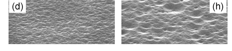
7 ZnO:Al films exhibit low resistivity of Ω cm and high Hall mobility up to 47 cm 2 /Vs. The excellent electrical quality of the ZnO:Al films is very similar to that of samples deposited from rotatable ceramic targets at high rate [3] and even to ZnO:Al films from laboratory developments sputtered with radio frequency (rf) excitation at rather low rate [2, 4] Etching behavior and surface morphologies As-grown and texture-etched ZnO:Al films show different topographies. Fig. 4 shows the morphologies of ZnO:Al films deposited at 300 C and PEM intensities of 20%, 30%, 40% and 50%, respectively, in as-grown (left) and post-etched states (right). As seen from Fig. 4 (a), the initial morphology of ZnO:Al film deposited at PEM intensity of 20% shows small crater structures with the feature size of 100 nm in diameter. The crater walls are formed by grains that have pyramidal shape or form ridges. This film represents a transition between fully pyramid-shaped to crater-like surfaces as both feature types are present. For a PEM intensity of 30% the features on the un-etched sample have crater-shape with typical diameters around 200 nm (Fig. 4 (b)). The surface of as grown ZnO:Al film deposited at 40% shows some wider but more shallow craters compared to films deposited at lower PEM intensity (Fig. 4 (c)). ZnO:Al films deposited at 50% show a rather flat surface with flat grains as shown in Fig. 4 (d). These ZnO:Al films also show different surface structures after a wet chemical etching step in dilute HCl as shown in Fig. 4 (e, f, g and h). The ZnO:Al film deposited at PEM intensity of 20% shows flat plateaus, 1 µm wide moon craters
8 and sharp spikes as shown in Fig. 4 (e). The samples deposited at PEM intensity of 30% and 40% show large conical craters of about 1 µm which are much more shallow for 40 % PEM intensity (Fig. 4 (f) and (g)). The ZnO:Al film deposited at PEM intensity of 50% (Fig. 4 (h)) shows similar craters to that of the PEM 40% film (Fig. 4 (g)), but the craters are smaller. Additionally, one can find small features which look similar to that on the initial as-grown surface even inside the craters shown in Fig. 4 (h). The surfaces of the samples deposited at different substrate temperatures and a constant PEM intensity of 35% are shown in Fig. 5 for the as-grown and etched states. Fig. 5 (a, b, and c) show the morphologies of as-grown films deposited at 250 C, 300 C and 350 C, respectively. For the samples deposited at 250 C, grains with pyramidal shape with nm bases are visible on the surface as shown in Fig. 5 (a). At 300 C and 350 C the grains become smaller and form distinct craters of various diameters on the surfaces (Fig. 5 (b and c)). Fig. 5 (d, e and f) show the corresponding ZnO:Al surfaces after etching. Fig. 5 (d) shows cliffy surface with feature sizes similar to the as-grown surface while for sample deposited at 300 C and 350 C many small shallow craters together with a few larger craters distribute on the surface (see Fig. 5 (e and f)). Surfaces of samples deposited above 300 C in metallic mode at high PEM intensities seem much flatter and more etch resistant compared to that of ZnO:Al films deposited at 250 C or close to the oxide mode. This is supported by the etching rates for the three series already discussed before (see Fig. 6). The etching rate
9 decreases with the increase of PEM intensity as well as with the increase of substrate temperature. Note the remarkable increase of etch rate by a factor of four by varying PEM intensity from 50% to 20% at 250 C. The high etch rate and corresponding surfaces after etching (Fig. 4(e) and Fig. 5 (d)) are attributed to much lower film compactness at low temperature or close to the oxide mode [9, 10, 16] Optical properties Fig. 7 shows the transmission and absorption after etching of ZnO:Al thin films deposited at 300 C and PEM intensities between 20-50%. All samples show a high optical transmission of more than 85% and a low absorption in the visible spectral range. The transmission in the near infrared (NIR) spectral range is affected by the free carrier absorption. Here it increases with higher PEM intensity, which is in good agreement with the trend for the carrier concentration extracted from Hall measurements (compare Fig. 2(c)) [10]. The corresponding transmission data vary conversely in this spectral range. The thicknesses of samples (given in the legend of Fig. 7) play a minor role in light absorption or transmission compared to the effect of carrier concentration. The transmission and absorption of samples prepared at 250 C and 350 C show a similar dependency on the PEM intensity (not shown). The absorption edge (as shown in Fig. 7) shifts towards shorter wavelengths with increasing PEM intensity. Based on the optical measurements, we extracted the optical energy gap of the 300 C series as plotted in Fig. 8. The band gap increases from 3.43 ev to 3.59 ev with increase of PEM intensity. In Fig. 9 the extracted
10 optical band gaps of PEM series for the investigated substrate temperatures are shown. All series show a similar trend of increasing band gap with PEM intensity. This is caused by the Burstein-Moss effect [17, 18] that enlarges the optical energy gap for higher carrier density. At high temperatures the slope and range of energy gaps decreases as was already observed for carrier density (see Fig. 2(c)). 4. Discussion ZnO:Al films with excellent electrical and optical properties were prepared. High optical transmittance of more than 85 % coincides with low resistivity of less than Ω cm. The low doping level together with high substrate temperature during sputter deposition lead to high charge carrier mobility at low carrier density to limit free carrier absorption in the NIR. These properties of ZnO:Al are very close to other publications [2, 9, 11 13] and will be appropriate for most applications. For solar cell application the surface texture after etching plays an important role. Thus we concentrate our discussion on the ZnO:Al surface properties. Taking a close look at the SEM images we propose a relationship between as-grown and post-etch surfaces. Some post-etched surfaces exhibit features similar to the initial surface structures. The small craters inside the larger ones of Fig. 4 (f) are of similar size and shape as the craters formed by adjacent grains on the as-grown surface. Similarly, the etched surface of the ZnO:Al sputtered at PEM intensity of 50% (Fig. 4 (h) is covered by small granular roughness, that might stem from the initial as-grown surface. Furthermore, the overall feature size of the ZnO:Al film sputtered at 250 C is similar
11 for initial and etched surface (Fig. 5 (a and d)). However, the shape is modified by the etching step. In contrast, the films prepared at high temperatures in Fig. 5 (e and f) do not clearly reveal features of the initial surface. Furthermore, the granular structure of the initial ZnO:Al film has vanished after etching on the plateaus between moon craters (Fig. 4 (e)) rather completely, even though the ground of the moon craters shows the features comparable to the as-grown surface. In conclusion, parts of the post-etched surface seem to be residues of the as-grown surface; however, the initial thickness is strongly reduced and thus the initial surface features must survive the etch process. Owen et al. investigated the etch attack in the initial stage and also found interrelation between crater formation during etching and characteristic features on the as-grown surface [19]. However, it is not yet possible to predict the etching behavior and crater evolution from as-grown ZnO:Al film properties. Most samples of this study show a relatively flat surface structure after chemical wet etching in dilute HCl and consequently, their Haze (Fig. 10) is low. The highest haze is achieved for the film deposited at 30% PEM intensity and 300 C substrate temperature. The corresponding surface structure is shown in Fig. 4 (f). Even though a high haze is no guarantee for good for light trapping in thin-film solar cells [20], we consider this surface structure together with the reasonable optical and electrical properties as most promising selection of our ZnO:Al films as transparent front contact in silicon based thin film solar cells. However, in order to successfully apply these high rate reactively sputtered ZnO:Al films into silicon based thin film solar cells, further improvement of the
12 surface structure is needed for the sake of a good light trapping effect inside solar cells [21]. 5. Conclusions ZnO:Al films were prepared by reactive sputter deposition from rotatable metallic targets. At high growth rate of close to 90 nm m/min low resistivity down to Ω cm and high Hall mobility up to 47 cm 2 /Vs were achieved. The excellent electrical properties are comparable to those of ZnO:Al deposited at high rate from rotatable ceramic targets and even to ZnO:Al films prepared at low rate. High transmission of more than 85% in the visible spectral range is obtained for all ZnO:Al films in this study. In addition, the absorption in NIR region is low due to low doping, high substrate temperature and sputtering in transition mode. The good optical and electrical properties, high deposition rate from cost effective metallic targets and high target utilization due to the use of tube targets make this process applicable for ZnO:Al production. A relationship between initial and post-etched surface topography is proposed. A prediction of the post-etched surface by investigating as-grown films would mark a great progress for quality control of sputtered ZnO:Al films in a production line. Acknowledgements The authors would like to thank our colleagues J. Worbs, H. Siekamnn and H. P. Bochem for great help in experimental support. Fruitful discussions with our project
13 partners W. Dewald, V. Sittinger, B. Szyszka, D. Köhl and F. Ruske are gratefully acknowledged. This study was financially supported by the German ministry BMU under contract No A.
14 Reference [1] B. Rech. H. Wagner. Appl. Phys. A 69 (1999) 155 [2] M. Berginski, J. Hüpkes, M. Schlute, G.. Schöpe, H. Stiebig, M. Wuttig. J. Appl. Phys. 101 (2007) [3] H. Zhu, E. Bunte, J. Hüpkes, H. Siekmann, S. M. Huang. Thin Solid Films 517 (2008) [4] E. Bunte, H. B. Zhu, J. Hüpkes. Proceeding of 23rd European Photovoltaic Solar Energy Conference, 1-5 September 2008, Valencia, Spain, p2105. [5] B. Szyszka. Thin Solid Films 351 (1999) 164. [6] B. Szyszka, V.Sittinger, X. Jiang, R.J. Hong, w. Werner, A. Pfug, M. Ruske, A. Lopp. Thin Solid Films 442(2003)179. [7] C. May, R. Menner, J. Strümpfel, M. Oertel, B. Specher. Surf. Coat. Technol (2003) 512. [8] J. Müller, G. Schöpe, O. Kluth, V. Sittinger, B. Szyszka, R. Geyer, P. Lechner, H. Schade, M. Ruske, G. Dittmar, H.-P. Bochem, Thin Solid Films 442 (2003) 158. [9] J. Hüpkes, B, Rech, S. Calnan, O. Kluth, U. Zastrow, H. Siekmann, M. Wuttig. Thin Solid Films 502(2006)286 [10] J. Hüpkes, B. Rech, O. Kluth, T. Repmann, B. Zwaygardt, J. Müller, R. Drese, M. Wuttig. Sol. Energy. Mater. Sol. Cells 90 (2006) [11] V. Sittinger, F. Ruske, A. Pflug, W. Dewald, B. Szyszka and G. Dittmar, Thin Solid Films 518 (2010) 3115.
15 [12] K. Sato, Y. Gotoh, Y. Hayashi, K. Adachi, H. Nishimura, Reports Res. Laboratory Asahi Glass Co. Ltd.,vol. 40, 1990, p [13] T. Minami, H. Nanto and S. Takata. Jpn. J. Appl. Phys 23 (1984) L280. [14] K. Tominaga, K. Kuroda and O. Tada. Jpn. J. Appl. Phys 27 (1988) [15] K. Ellmer, J. Phys. D: Appl. Phys. 34 (2001) [16] O. Kluth, G. Schöpe, J. Hüpkes, C. Agashe, J. Müller, B. Rech, Thin Solid Films 442 (2003) 80. [17] E. Burstein. Phys. Rev. 93 (1954) 632. [18] T. S. Moss. Proc. Phys. Rev B 67(1954)775 [19] J. I. Owen, J. Hüpkes, E. Bunte, MRS Symposium proceedings 1153 (2009) A07-08 [20] P. Lechner, R. Geyer, H. Schade, B. Rech, O. Kluth and H. Stiebig, 19th European Photovoltaic Solar Energy Conference, 2004, Paris, France, p [21] B. Rech, T. Repmann, V. M. N. van den Donker, M. Berginski, T. Kilper, J. Hüpkes, S. Calnan, H. Stiebig, S. Wieder. Thin Solid Film (2006) 548
16 Figure captions Fig. 1 Relationship between oxygen gas flow and plasma emission monitoring (PEM) intensity, which is characterized by intensity of 307 nm zinc emission line during the reactive sputtering. Fig. 2 Dependence of deposition rate (a) and electrical properties: resistivity (b), carrier concentration (c) and Hall mobility (d) of ZnO:Al films on substrate temperature and PEM intensity. Fig. 3 Working pressure and oxygen partial pressure as a function of PEM intensity. Fig. 4 SEM images of as-grown ZnO:Al films deposited at 300 C and different PEM intensity: (a) 20%, (b) 30%, (c) 40%, (d) 50%. The SEM images of corresponding after-etched ZnO:Al films are shown in (e) 20%, (f) 30%, (g) 40% and (h) 50% Fig. 5 SEM images of as-grown ZnO:Al films deposited at PEM intensity of 35% and different substrate temperatures: (a) 250 C, (b) 300 C, (c) 350 C. The SEM images of corresponding after-etched ZnO:Al films are shown in (d) 250 C, (e) 300 C, (f) 350 C as well. Fig. 6 Etching rate of ZnO:Al films reactively sputtered at different substrate temperatures as a function of PEM intensity. Fig. 7 Light transmission and absorption of ZnO:Al films reactively sputtered at 300 C and different PEM intensities. Fig. 8 (α) 2 as a function of (hν) for ZnO:Al films sputtered at 300 C and different PEM intensities, where α is absorption coefficient and (hν) is the incident photon energy.
17 Fig. 9 Optical band gaps of ZnO:Al films sputtered at different substrate temperatures and different PEM intensities. Fig. 10 Haze of ZnO:Al films reactively sputtered at 300 C and different PEM intensities.
18 Zhu_ Fig. 1. tif Metallic mode Oxygen gas flow control mode PEM intensity control mode PEM intensity (%) Oxide mode to Metallic mode Metallic mode to Oxide mode Oxide mode Transition mode Oxygen gas flow (sccm)
19 Zhu_ Fig. 2. tif Depostion rate (nm m/min) C 300 C 250 C a 350 C 300 C 250 C b Resistivity (10 4 Ω cm) Carrier Concentration (10 20 cm -3 ) PEM intensity (%) 350 C 300 C 250 C c PEM intensity (%) 350 C 300 C 250 C d Mobility ( cm 2 / Vs) PEM intensity (%) PEM intensity (%)
20 Zhu_Fig. 3. tif Working pressure (Pa) C 300 C 250 C Oxygen partial presssure (mpa) PEM intensity (%)


21 Zhu_Fig. 4. tif Surface and Coatings Technology 205 (2010),


,")
22 Zhu_ Fig. 5. tif Surface and Coatings Technology 205 (2010),
23 Zhu_ Fig. 6. tif 20 Etching rate (nm/s) C 300 C 250 C PEM intensiy (%)
24 Zhu_ Fig. 7. tif Transmission and Absorption (%) PEM intensity Thickness 20% 779 nm 30% 677 nm 40% 656 nm 50% 561 nm Absorption Wavelength (nm) Transmission
25 Zhu_ Fig. 8. tif (α) 2 (10 10 cm -2 ) PEM intensity 20% 25% 30% 35% 40% 50% 3.54 ev 3.59 ev ev 3.50 ev 3.47eV 3.43eV hν (ev)
26 Zhu_ Fig. 9. tif 3.72 Optical band gap (ev) C 300 C 250 C PEM intensity (%)
27 Zhu_ Fig. 10. tif Haze PEM intensity 20% 25% 30% 35% 40% 50% Wavelength (nm)
Sputtered Zinc Oxide Films for Silicon Thin Film Solar Cells: Material Properties and Surface Texture
 Poster FVS Workshop 2002 Sputtered Zinc Oxide Films for Silicon Thin Film Solar Cells: Material Properties and Surface Texture Texture etching of sputtered ZnO:Al films has opened up a variety of possibilities
ZnO-based Transparent Conductive Oxide Thin Films
 IEEE EDS Mini-colloquium WIMNACT 32 ZnO-based Transparent Conductive Oxide Thin Films Weijie SONG Ningbo Institute of Material Technology and Engineering, Chinese Academy of Sciences, Ningbo, P. R. China
Linear Plasma Sources for Surface Modification and Deposition for Large Area Coating
 Linear Plasma Sources for Surface Modification and Deposition for Large Area Coating Dr Tony Williams Gencoa Ltd, UK Victor Bellido-Gonzalez, Dr Dermot Monaghan, Dr Joseph Brindley, Robert Brown SVC 2016,
AC Reactive Sputtering with Inverted Cylindrical Magnetrons
 AC Reactive Sputtering with Inverted Cylindrical Magnetrons D.A. Glocker, Isoflux Incorporated, Rush, NY; and V.W. Lindberg and A.R. Woodard, Rochester Institute of Technology, Rochester, NY Key Words:
Growth Of TiO 2 Films By RF Magnetron Sputtering Studies On The Structural And Optical Properties
 Journal of Multidisciplinary Engineering Science and Technology (JMEST) Growth Of TiO 2 Films By RF Magnetron Sputtering Studies On The Structural And Optical Properties Ahmed K. Abbas 1, Mohammed K. Khalaf
EFFECT OF HYDROGEN, CERIUM AND TUNGSTEN DOPING ON INDIUM OXIDE THIN FILMS FOR HETEROJUNCTION SOLAR CELLS
 EFFECT OF HYDROGEN, CERIUM AND TUNGSTEN DOPING ON INDIUM OXIDE THIN FILMS FOR HETEROJUNCTION SOLAR CELLS A. Valla, P. Carroy, F. Ozanne, G. Rodriguez & D. Muñoz 1 OVERVIEW Description of amorphous / crystalline
Deposition-Temperature Effects on AZO Thin Films Prepared by RF Magnetron Sputtering and Their Physical Properties
 Journal of the Korean Physical Society, Vol. 49, December 2006, pp. S584 S588 Deposition-Temperature Effects on AZO Thin Films Prepared by RF Magnetron Sputtering and Their Physical Properties Jeung Hun
Electrical, optical and structural properties of transparent and conducting ZnO thin. films doped with Al and F by rf magnetron sputter
 Electrical, optical and structural properties of transparent and conducting ZnO thin films doped with Al and F by rf magnetron sputter B.G. Choi 1), I.H. Kim *, D.H Choi 1), K.S. Lee, T.S. Lee, B. Cheong,
Plasma Activated EB-PVD of Titanium and its Compounds by Means of Large Area SAD
 AIMCAL 2005 Myrtle Beach, SC, USA, October 19th, 2005 Plasma Activated EB-PVD of Titanium and its Compounds by Means of Large Area SAD E. Reinhold, C. Steuer VON ARDENNE Anlagentechnik GmbH, Dresden, Germany
SULPHUR INDUCED CHANGES IN THE BAND GAP ENERGY AND THE TRANSPARENCY WINDOW OF CHEMICAL BATH DEPOSITED ZnO:S THIN FILMS
 Chalcogenide Letters Vol. 1, No. 8, August 015, p. 99-406 SULPHUR INDUCED CHANGES IN THE BAND GAP ENERGY AND THE TRANSPARENCY WINDOW OF CHEMICAL BATH DEPOSITED ZnO:S THIN FILMS R. CHIKWENZE a*, S. EZUGWU
A Plasma Emission Controller for Reactive. Magnetron Sputtering of Titanium Dioxide Films
 Adv. Theor. Appl. Mech., Vol. 5, 2012, no. 1, 1-10 A Plasma Emission Controller for Reactive Magnetron Sputtering of Titanium Dioxide Films Raad A. Swady DMPS, College of Arts & Sciences, University of
Thin Films: Sputtering Systems (Jaeger Ch 6 & Ruska Ch 7,) Sputtering: gas plasma transfers atoms from target to substrate Can deposit any material
 Sputtering: gas plasma transfers atoms from target to substrate Can deposit any material") Thin Films: Sputtering Systems (Jaeger Ch 6 & Ruska Ch 7,) Sputtering: gas plasma transfers atoms from target to substrate Can deposit any material on any substrate (in principal) Start with pumping down
Thin Films: Sputtering Systems (Jaeger Ch 6 & Ruska Ch 7,) Sputtering: gas plasma transfers atoms from target to substrate Can deposit any material on any substrate (in principal) Start with pumping down
Metallization deposition and etching. Material mainly taken from Campbell, UCCS
 Metallization deposition and etching Material mainly taken from Campbell, UCCS Application Metallization is back-end processing Metals used are aluminum and copper Mainly involves deposition and etching,
Investigations on Properties of (ZnO:Al) Films Prepared by RF/DC Co-sputtering
 Films Prepared by RF/DC Co-sputtering") TELKOMNIKA, Vol.10, No.5, September 2012, pp. 947~952 e-issn: 2087-278X accredited by DGHE (DIKTI), Decree No: 51/Dikti/Kep/2010 947 Investigations on Properties of (ZnO:Al) Films Prepared by RF/DC Co-sputtering
TELKOMNIKA, Vol.10, No.5, September 2012, pp. 947~952 e-issn: 2087-278X accredited by DGHE (DIKTI), Decree No: 51/Dikti/Kep/2010 947 Investigations on Properties of (ZnO:Al) Films Prepared by RF/DC Co-sputtering
Transparent Conductive Oxides in Thin Film Photovoltaics
 Journal of Physics: Conference Series OPEN ACCESS Transparent Conductive Oxides in Thin Film Photovoltaics To cite this article: Frank U Hamelmann 2014 J. Phys.: Conf. Ser. 559 012016 View the article
Applied Research for Vacuum Web Coating: What is Coming Next?
 Applied Research for Vacuum Web Coating: What is Coming Next? Matthias Fahland, John Fahlteich, Steffen Günther, Manuela Junghähnel, Claus Luber, Nicolas Schiller, Cindy Steiner, Steffen Straach, Michiel
Transactions on Engineering Sciences vol 2, 1993 WIT Press, ISSN
 A study of thin-film continuous coating process by vapour deposition P. Gimondo," F. Arezzo,* B. Grifoni,* G. Jasch& "Centra Sviluppo Materiali SpA, Via di Castel & Von Ardenne Anlagentchnik GmbH, Plattleite
Effect of Enhanced Plasma Density on the Properties of Aluminium Doped Zinc Oxide Thin Films Produced by DC Magnetron Sputtering
 J. Mater. Sci. Technol., 2011, 27(5), 393-397. Effect of Enhanced Plasma Density on the Properties of Aluminium Doped Zinc Oxide Thin Films Produced by DC Magnetron Sputtering Jun Gong, Xiaobo Zhang, Zhiliang
The growth of patterned ceramic thin films from polymer precursor solutions Göbel, Ole
 University of Groningen The growth of patterned ceramic thin films from polymer precursor solutions Göbel, Ole IMPORTANT NOTE: You are advised to consult the publisher's version (publisher's PDF) if you
Nanostructured Engineered Materials With High Magneto-optic Performance For Integrated Photonics Applications
 Edith Cowan University Research Online School of Engineering Publications 28 Nanostructured Engineered Materials With High Magneto-optic Performance For Integrated Photonics Applications Mikhail Vasiliev
Structure and optical properties of M/ZnO (M=Au, Cu, Pt) nanocomposites
 nanocomposites") Solar Energy Materials & Solar Cells 8 () 339 38 Structure and optical properties of M/ (M=Au, Cu, Pt) nanocomposites U. Pal a,b, *, J. Garc!ıa-Serrano a, G. Casarrubias-Segura a, N. Koshizaki c, T. Sasaki
Solar Energy Materials & Solar Cells 8 () 339 38 Structure and optical properties of M/ (M=Au, Cu, Pt) nanocomposites U. Pal a,b, *, J. Garc!ıa-Serrano a, G. Casarrubias-Segura a, N. Koshizaki c, T. Sasaki
Simple method for formation of nanometer scale holes in membranes. E. O. Lawrence Berkeley National Laboratory, Berkeley, CA 94720
 Simple method for formation of nanometer scale holes in membranes T. Schenkel 1, E. A. Stach, V. Radmilovic, S.-J. Park, and A. Persaud E. O. Lawrence Berkeley National Laboratory, Berkeley, CA 94720 When
Study of a-sige:h Films and n-i-p Devices used in High Efficiency Triple Junction Solar Cells.
 Study of a-sige:h Films and n-i-p Devices used in High Efficiency Triple Junction Solar Cells. Pratima Agarwal*, H. Povolny, S. Han and X. Deng. Department of Physics and Astronomy, University of Toledo,
Applications of Successive Ionic Layer Adsorption and Reaction (SILAR) Technique for CZTS Thin Film Solar Cells
 Technique for CZTS Thin Film Solar Cells") NANO VISION An International Open Free Access, Peer Reviewed Research Journal www.nano-journal.org ISSN 2231-2579 (Print) ISSN 2319-7633 (Online) Abbr: Nano Vision. 2013, Vol.3(3): Pg.235-239 Applications
NANO VISION An International Open Free Access, Peer Reviewed Research Journal www.nano-journal.org ISSN 2231-2579 (Print) ISSN 2319-7633 (Online) Abbr: Nano Vision. 2013, Vol.3(3): Pg.235-239 Applications
Excimer Laser Annealing of Hydrogen Modulation Doped a-si Film
 Materials Transactions, Vol. 48, No. 5 (27) pp. 975 to 979 #27 The Japan Institute of Metals Excimer Laser Annealing of Hydrogen Modulation Doped a-si Film Akira Heya 1, Naoto Matsuo 1, Tadashi Serikawa
Thin film silicon technology. Cosimo Gerardi 3SUN R&D Tech. Coordinator
 Thin film silicon technology Cosimo Gerardi 3SUN R&D Tech. Coordinator 1 Outline Why thin film Si? Advantages of Si thin film Si thin film vs. other thin film Hydrogenated amorphous silicon Energy gap
Mater. Res. Soc. Symp. Proc. Vol Materials Research Society
 Mater. Res. Soc. Symp. Proc. Vol. 940 2006 Materials Research Society 0940-P13-12 A Novel Fabrication Technique for Developing Metal Nanodroplet Arrays Christopher Edgar, Chad Johns, and M. Saif Islam
Optical and Electrical Characterization of CuO Thin Films as Absorber Material for Solar Cell Applications
 American Journal of Condensed Matter Physics 16, 6(1): 1-6 DOI: 1.5923/j.ajcmp.11.1 Optical and Electrical Characterization of CuO Thin Films as Absorber Material for Solar Cell Applications K. S. Wanjala
 This article was originally published in a journal published by Elsevier, and the attached copy is provided by Elsevier for the author s benefit and for the benefit of the author s institution, for non-commercial
Surface Analysis of Electrochromic Switchable Mirror Glass Based on Magnesium-Nickel Thin Film in Accelerated Degradation Test
 Materials Transactions, Vol. 52, No. 3 (2011) pp. 464 to 468 #2011 The Japan Institute of Metals Surface Analysis of Electrochromic Switchable Mirror Glass Based on Magnesium-Nickel Thin Film in Accelerated
Roll-to-roll Technology for Transparent High Barrier Films
 Roll-to-roll Technology for Transparent High Barrier Films Presented at the AIMCAL Fall Technical Conference, October 19-22, 2008, Myrtle Beach, SC, USA Nicolas Schiller, John Fahlteich, Matthias Fahland,
Electronic structure and x-ray-absorption near-edge structure of amorphous Zr-oxide and Hf-oxide thin films: A first-principles study
 JOURNAL OF APPLIED PHYSICS 97, 073519 2005 Electronic structure and x-ray-absorption near-edge structure of amorphous Zr-oxide and Hf-oxide thin films: A first-principles study SungKwan Kim, a Yangsoo
LOT. Contents. Introduction to Thin Film Technology. Chair of Surface and Materials Technology
 Introduction to Thin Film Contents 1. Introduction and Application Examples (2h) 2. Preparation of Thin Films by PVD (Physical Vapor Deposition) (6h) 2.1 Vacuum Technique (1h) 2.1.1 Kinetics of Gases 2.1.2
HiPIMS Deposition of Metal and Oxide Coatings
 HiPIMS Deposition of Metal and Oxide Coatings 1 GT West, 1 PJ Kelly, 1 P Barker, 2 JW Bradley and 2 A Mishra 1. Surface Engineering Group, Manchester Metropolitan University, UK 2. Electrical Engineering
DEVELOPMENT OF HIGH EFFICIENCY FLEXIBLE CdTe SOLAR CELLS
 DEVELOPMENT OF HIGH EFFICIENCY FLEXIBLE CdTe SOLAR CELLS A.Romeo, M. Arnold, D.L. Bätzner, H. Zogg and A.N. Tiwari* Thin Films Physics Group, Laboratory for Solid State Physics, Swiss Federal Institute
Comparison of DC and RF sputtered aluminium-doped zinc oxide for photovoltaic applications
 Loughborough University Institutional Repository Comparison of and sputtered aluminium-doped zinc oxide for photovoltaic applications This item was submitted to Loughborough University's Institutional
Alternative Methods of Yttria Deposition For Semiconductor Applications. Rajan Bamola Paul Robinson
 Alternative Methods of Yttria Deposition For Semiconductor Applications Rajan Bamola Paul Robinson Origin of Productivity Losses in Etch Process Aggressive corrosive/erosive plasma used for etch Corrosion/erosion
Oxide Growth. 1. Introduction
 Oxide Growth 1. Introduction Development of high-quality silicon dioxide (SiO2) has helped to establish the dominance of silicon in the production of commercial integrated circuits. Among all the various
PARAMETER EFFECTS FOR THE GROWTH OF THIN POROUS ANODIC ALUMINUM OXIDES
 10.1149/1.2794473, The Electrochemical Society PARAMETER EFFECTS FOR THE GROWTH OF THIN POROUS ANODIC ALUMINUM OXIDES S. Yim a, C. Bonhôte b, J. Lille b, and T. Wu b a Dept. of Chem. and Mat. Engr., San
PRECISION OPTICAL FILTERS BY EOSS - ENHANCED OPTICAL SPUTTERING SYSTEM. Fraunhofer
 PRECISION OPTICAL FILTERS BY EOSS - ENHANCED OPTICAL SPUTTERING SYSTEM EOSS ENHANCED OPTICAL SPUTTERING SYSTEM Fraunhofer IST, Braunschweig Contact: Dr. M. Vergöhl +49 531 2155 640 EOSS Coating System
High Rate low pressure PECVD for barrier and optical coatings
 High Rate low pressure PECVD for barrier and optical coatings, Matthias Fahland, John Fahlteich, Björn Meyer, Steffen Straach, Nicolas Schiller Outline Introduction PECVD New developments magpecvd arcpecv
Optical Coatings. Photonics 4 Luxury Coatings , Genève. Dr. Andreas Bächli Head of Optical Coatings at RhySearch, Buchs (SG)
") Optical Coatings Photonics 4 Luxury Coatings 21.06.2017, Genève Dr. Andreas Bächli Head of Optical Coatings at RhySearch, Buchs (SG) RhySearch The Research- and Innovation Center in the Rhine Valley RhySearch
Optical Coatings Photonics 4 Luxury Coatings 21.06.2017, Genève Dr. Andreas Bächli Head of Optical Coatings at RhySearch, Buchs (SG) RhySearch The Research- and Innovation Center in the Rhine Valley RhySearch
Thin film photovoltaics: industrial strategies for increasing the efficiency and reducing costs
 STATO E PROSPETTIVE DEL FOTOVOLTAICO IN ITALIA 26 giugno 2014 ENEA Via Giulio Romano n. 41, Roma Thin film photovoltaics: industrial strategies for increasing the efficiency and reducing costs Anna Battaglia,
II. NEG THIN FILM DEPOSITION
 Deposition of Non-Evaporable Getter Thin Films and Vacuum Pumping Performances Ankit Sur Engineering Department, Wayne State University, Detroit, MI 48202 The ERL (Energy Recovery Linac) proposed at Cornell
Coatings. Ion Assisted Deposition (IAD) process Advance Plasma Source (APS) plasma-ion assisted Deposition. Coatings on Optical Fibers
 process Advance Plasma Source (APS) plasma-ion assisted Deposition. Coatings on Optical Fibers") Anti-Reflection Custom Ion Assisted Deposition (IAD) process Advance Plasma Source (APS) plasma-ion assisted Deposition Anti-Reflection on Optical Fibers OptoSigma supplies a wide selection of optical
Anti-Reflection Custom Ion Assisted Deposition (IAD) process Advance Plasma Source (APS) plasma-ion assisted Deposition Anti-Reflection on Optical Fibers OptoSigma supplies a wide selection of optical
Study on Properties of Silicon Oxycarbide Thin Films Prepared by RF Magnetron Sputtering Tao Chen a, Maojin Dong, Jizhou Wang,Ling Zhang and Chen Li
 Study on Properties of Silicon Oxycarbide Thin Films Prepared by RF Magnetron Sputtering Tao Chen a, Maojin Dong, Jizhou Wang,Ling Zhang and Chen Li Science and Technology on Surface Engineering Laboratory,
Thin Film Characterizations Using XRD The Cases of VO2 and NbTiN
 Thin Film Characterizations Using XRD The Cases of VO2 and NbTiN A thesis submitted in partial fulfillment of the requirement for the degree of Bachelor of Arts / Science in Physics from The College of
Solar Cells and Photosensors.
 Designing Photonic Crystals in Strongly Absorbing Material for Applications in Solar Cells and Photosensors. Minda Wagenmaker 1, Ebuka S. Arinze 2, Botong Qiu 2, Susanna M. Thon 2 1 Mechanical Engineering
Supplementary Material (ESI) for Chemical Communications This journal is (c) The Royal Society of Chemistry 2009
 for Chemical Communications This journal is (c) The Royal Society of Chemistry 2009") Supplementary Information Silver Nanoparticles with Planar Twinned Defects: Effect of Halides for Precise Tuning of Plasmon Absorption from 400 to >900 nm by Nicole Cathcart, Andrew J. Frank and Vladimir
Supplementary Information Silver Nanoparticles with Planar Twinned Defects: Effect of Halides for Precise Tuning of Plasmon Absorption from 400 to >900 nm by Nicole Cathcart, Andrew J. Frank and Vladimir
Understanding Optical Coatings For Military Applications
 Understanding Optical Coatings For Military Applications By Trey Turner, Chief Technology Officer, REO Virtually all optical components used in military applications, such as target designation, rangefinding
Structural, electrical, and optical properties of ZnInO alloy thin films
 Structural, electrical, and optical properties of ZnInO alloy thin films Cai Xi-Kun( ), Yuan Zi-Jian( ), Zhu Xia-Ming( ), Wang Xiong( ), Zhang Bing-Po( ), Qiu Dong-Jiang( ), and Wu Hui-Zhen( ) Department
SUPPLEMENTARY INFORMATION
 In the format provided by the authors and unedited. ARTICLE NUMBER: 16178 DOI: 10.1038/NENERGY.2016.178 Enhanced Stability and Efficiency in Hole-Transport Layer Free CsSnI3 Perovskite Photovoltaics Supplementary
Preparation and Characterization of Micro-Crystalline Hydrogenated Silicon Carbide p-layers
 Preparation and Characterization of Micro-Crystalline Hydrogenated Silicon Carbide p-layers Erten Eser, Steven S. Hegedus and Wayne A. Buchanan Institute of Energy Conversion University of Delaware, Newark,
Ultra High Barrier Coatings by PECVD
 Society of Vacuum Coaters 2014 Technical Conference Presentation Ultra High Barrier Coatings by PECVD John Madocks & Phong Ngo, General Plasma Inc., 546 E. 25 th Street, Tucson, Arizona, USA Abstract Silicon
DEPOSITION OF Al 2 O 3 ON CERAMIC SUBSTRATES BY PECVD METHOD. Lucie Špirková a Vlastimil Brožek a Jean Durand b
 DEPOSITION OF Al 2 O 3 ON CERAMIC SUBSTRATES BY PECVD METHOD Lucie Špirková a Vlastimil Brožek a Jean Durand b a) Institute of Chemical Technology, 166 28 Prague, Czech Republic b) Laboratoire des Matériaux
Transmission Mode Photocathodes Covering the Spectral Range
 Transmission Mode Photocathodes Covering the Spectral Range 6/19/2002 New Developments in Photodetection 3 rd Beaune Conference June 17-21, 2002 Arlynn Smith, Keith Passmore, Roger Sillmon, Rudy Benz ITT
Light Trapping Enhancement in Thin Film Silicon Solar Cell with Different Back Reflector
 International Journal of Electrical Components and Energy Conversion 2017; 3(5): 83-87 http://www.sciencepublishinggroup.com/j/ijecec doi: 10.11648/j.ijecec.20170305.11 ISSN: 2469-8040 (Print); ISSN: 2469-8059
Visualization and Control of Particulate Contamination Phenomena in a Plasma Enhanced CVD Reactor
 Visualization and Control of Particulate Contamination Phenomena in a Plasma Enhanced CVD Reactor Manabu Shimada, 1 Kikuo Okuyama, 1 Yutaka Hayashi, 1 Heru Setyawan, 2 and Nobuki Kashihara 2 1 Department
Optical Properties of Vacuum Evaporated WO 3 Thin Films
 Abstract Research Journal of Chemical Sciences ISSN 2231-606X. Optical Properties of Vacuum Evaporated WO 3 Thin Films Rao M.C. 1 and Hussain O.M. 2 1 Department of Physics, Andhra Loyola College, Vijayawada
Advanced Sheet-to-Sheet and Roll-to-Roll thin-film processing on ultra-thin flexible glass for flexible electronic devices
 Advanced Sheet-to-Sheet and Roll-to-Roll thin-film processing on ultra-thin flexible glass for flexible electronic devices M. Junghaehnel 1, J. Westphalen 1, F. Naumann 2, G. Lorenz 2, M. Fahland 1, S.
HiPIMS Technology: advantages and disadvantages
 Vacuum plasma technology HiPIMS Technology: advantages and disadvantages Cr - DC Cr - HiPIMS Alessandro Patelli alessandro.patelli@venetonanotech.it Outline 1. What is HiPIMS Ti target surface 2. What
Ag Ti Alloy Used in ITO Metal ITO Transparency Conductive Thin Film with Good Durability against Moisture
 Materials Transactions, Vol. 46, No. 11 (2005) pp. 2536 to 25 #2005 The Japan Institute of Metals EXPRESS REGULAR ARTICLE Ag Ti Alloy Used in ITO Metal ITO Transparency Conductive Thin Film with Good Durability
Aluminium-doped zinc oxide deposited by ultrasonic spray pyrolysis for thin film solar cell applications
 Aluminium-doped zinc oxide deposited by ultrasonic spray pyrolysis for thin film solar cell applications Panagiota Arnou, Jake W. Bowers and John M. Walls CREST (Centre for Renewable Energy Systems Technology),
Multiphoton lithography based 3D micro/nano printing Dr Qin Hu
 Multiphoton lithography based 3D micro/nano printing Dr Qin Hu EPSRC Centre for Innovative Manufacturing in Additive Manufacturing University of Nottingham Multiphoton lithography Also known as direct
Fabrication Technology
 Fabrication Technology By B.G.Balagangadhar Department of Electronics and Communication Ghousia College of Engineering, Ramanagaram 1 OUTLINE Introduction Why Silicon The purity of Silicon Czochralski
Challenges for Commercially viable Transparent Conductive Oxide Layers
 Challenges for Commercially viable Transparent Conductive Oxide Layers Arkema Inc. 900 First Ave., King of Prussia, PA 19406 R. Y. Korotkov, L. Fang, P. Ricou, M. Bluhm, J. Coffey, C. Polsz and G. Silverman
Structural and optical properties of CuO thin films prepared via R.F.magnetron sputtering
 Structural and optical properties of CuO thin films prepared via R.F.magnetron sputtering Riyam A. Hammoodi 1, Assist. Prof.Dr.Ahmed K. Abbas 1 and Prof. Dr.Abdulhussein K.Elttayef 2 1 University of Wasit,
Light-Induced Degradation of Thin Film Silicon Solar Cells
 Journal of Physics: Conference Series PAPER OPEN ACCESS Light-Induced Degradation of Thin Film Silicon Solar Cells To cite this article: F U Hamelmann et al 2016 J. Phys.: Conf. Ser. 682 012002 View the
EFFECT OF DEPOSITION TIME ON CHEMICAL BATH DEPOSITION PROCESS AND THICKNESS OF BaSe THIN FILMS.
 Journal of Optoelectronics and Biomedical Materials Vol. 3 Issue 4, October-December 2011 p. 81-85 EFFECT OF DEPOSITION TIME ON CHEMICAL BATH DEPOSITION PROCESS AND THICKNESS OF BaSe THIN FILMS. N.A. OKEREKE
Fabrication of CdTe thin films by close space sublimation
 Loughborough University Institutional Repository Fabrication of CdTe thin films by close space sublimation This item was submitted to Loughborough University's Institutional Repository by the/an author.
Optical characterization of an amorphoushydrogenated carbon film and its application in phase modulated diffractive optical elements
 Optical characterization of an amorphoushydrogenated carbon film and its application in phase modulated diffractive optical elements G. A. Cirino a, P. Verdonck a, R. D. Mansano a, L. G. Neto b a LSI-PEE-EPUSP
Characterization Of Aluminum Doped Zinc Oxide Thin Films For Photovoltaic Applications
 University of Central Florida Electronic Theses and Dissertations Masters Thesis (Open Access) Characterization Of Aluminum Doped Zinc Oxide Thin Films For Photovoltaic Applications 2010 Bojanna P. Shantheyanda
Vacuum Equipment for TCO and AR Coatings Deposition by Reactive Magnetron Sputtering
 Vacuum Equipment for TCO and AR Coatings Deposition by Reactive Magnetron Sputtering E. Yadin; V. Kozlov; E. Machevskis, Sidrabe, Inc., 17 Krustpils str.,riga, LV1073, Latvia. Tel: +371 7249806, Fax: +371
Basic efficiency limits, recent experimental results and novel light-trapping schemes in a-si:h, lc-si:h and micromorph tandem solar cells
 Published in Journal of Non-Crystalline Solids 338-34, 639-645, 24 which should be used for any reference to this work 1 Basic efficiency limits, recent experimental results and novel light-trapping schemes
Lecture 12. Physical Vapor Deposition: Evaporation and Sputtering Reading: Chapter 12. ECE Dr. Alan Doolittle
 Lecture 12 Physical Vapor Deposition: Evaporation and Sputtering Reading: Chapter 12 Evaporation and Sputtering (Metalization) Evaporation For all devices, there is a need to go from semiconductor to metal.
Gridless end-hall. Ion Sources. For Ion Assisted Thin Film Deposition & Substrate Cleaning
 Gridless end-hall Ion Sources For Ion Assisted Thin Film Deposition & Substrate Cleaning End-Hall Ion Sources mark I Ion Source The Mark I End-Hall is ideal for small research and development and pilot
"ITO Film Trend for Touch Panel Applications"
 AIMCAL Web Coating Conference 2011 October 23-26 Reno, Nevada USA 1 "ITO Film Trend for Touch Panel Applications" Teijin Chemicals Ltd. Haruhiko Itoh 2 Content 1. Structure and Features of TCF 2. Touch
Processing guidelines
 Processing guidelines mr-uvcur21 series UV-curable Polymer for UV-based Nanoimprint Lithography Characteristics mr-uvcur21 is a liquid UV-curable polymer system with low viscosity and high curing rate
Recrystallization in CdTe/CdS
 Thin Solid Films 361±362 (2000) 420±425 www.elsevier.com/locate/tsf Recrystallization in CdTe/CdS A. Romeo, D.L. BaÈtzner, H. Zogg, A.N. Tiwari* Thin Film Physics Group, Institute of Quantum Electronics,
Electrical and Optical Properties of TiN Thin Films
 ISSN -68, Inorganic Materials,, Vol., No., pp.. Pleiades Publishing, Ltd.,. Original Russian Text M.N. Solovan, V.V. Brus, E.V. Maistruk, P.D. Maryanchuk,, published in Neorganicheskie Materialy,, Vol.,
Atomic Layer Deposition
 Atomic Layer Deposition Ville Malinen R&D Engineer Nanopinnoitteita koneenrakentajille 2010 1 Introduction 1) Overview of Beneq 2) Atomic Layer Deposition (ALD), to deposit thin films, which Are dense
Presented at the 28th European PV Solar Energy Conference and Exhibition, 30 September 4 October, 2013, Paris, France
 INTEGRATING DIFFRACTIVE REAR SIDE STRUCTURES FOR LIGHT TRAPPING INTO CRYSTALLINE SILICON SOLAR CELLS J. Eisenlohr 1*, H. Hauser 1, J. Benick 1, A. Mellor 2, B. Bläsi 1, J.C. Goldschmidt 1, M. Hermle 1
Amorphous Silicon Solar Cells
 The Birnie Group solar class and website were created with much-appreciated support from the NSF CRCD Program under grants 0203504 and 0509886. Continuing Support from the McLaren Endowment is also greatly
CREOL, The College of Optics & Photonics, University of Central Florida
 Metal Substrate Induced Control of Ag Nanoparticle Plasmon Resonances for Tunable SERS Substrates Pieter G. Kik 1, Amitabh Ghoshal 1, Manuel Marquez 2 and Min Hu 1 1 CREOL, The College of Optics and Photonics,
In-Situ Low-Angle Cross Sectioning: Bevel Slope Flattening due to Self-Alignment Effects
 In-Situ Low-Angle Cross Sectioning: Bevel Slope Flattening due to Self-Alignment Effects UWE SCHEITHAUER SIEMENS AG, CT MM 7, Otto-Hahn-Ring 6, 81739 München, Germany Phone: + 49 89 636 44143 E-mail: uwe.scheithauer@siemens.com
Specimen configuration
 APPLICATIONNOTE Model 1040 NanoMill TEM specimen preparation system Specimen configuration Preparing focused ion beam (FIB) milled specimens for submission to Fischione Instruments. The Model 1040 NanoMill
High performance radio frequency generator technology for the Thermo Scientific icap 7000 Plus Series ICP-OES
 TECHNICAL NOTE 43334 High performance radio frequency generator technology for the Thermo Scientific icap 7000 Plus Series ICP-OES Keywords Free-running, Plasma, RF generator, Solid-state Using inductively
EE40 Lec 22. IC Fabrication Technology. Prof. Nathan Cheung 11/19/2009
 Suggested Reading EE40 Lec 22 IC Fabrication Technology Prof. Nathan Cheung 11/19/2009 300mm Fab Tour http://www-03.ibm.com/technology/manufacturing/technology_tour_300mm_foundry.html Overview of IC Technology
Plasma-Enhanced Chemical Vapor Deposition
 Plasma-Enhanced Chemical Vapor Deposition Steven Glenn July 8, 2009 Thin Films Lab 4 ABSTRACT The objective of this lab was to explore lab and the Applied Materials P5000 from a different point of view.
Reactor wall plasma cleaning processes after InP etching in Cl 2 /CH 4 /Ar ICP discharge
 Reactor wall plasma cleaning processes after InP etching in Cl 2 /CH 4 /Ar ICP discharge R. Chanson a, E. Pargon a, M. Darnon a, C. Petit Etienne a, S. David a, M. Fouchier a, B. Glueck b, P. Brianceau
Specimen Preparation Technique for a Microstructure Analysis Using the Focused Ion Beam Process
 Specimen Preparation Technique for a Microstructure Analysis Using the Focused Ion Beam Process by Kozue Yabusaki * and Hirokazu Sasaki * In recent years the FIB technique has been widely used for specimen
Available online at ScienceDirect. Energy Procedia 55 (2014 )
") Available online at www.sciencedirect.com ScienceDirect Energy Procedia 55 (2014 ) 702 707 4th International Conference on Silicon Photovoltaics, SiliconPV 2014 Observation of the contact formation of
Available online at www.sciencedirect.com ScienceDirect Energy Procedia 55 (2014 ) 702 707 4th International Conference on Silicon Photovoltaics, SiliconPV 2014 Observation of the contact formation of
Characterization of thin Gd 2 O 3 magnetron sputtered layers
 Characterization of thin Gd 2 O 3 magnetron sputtered layers Jacek Gryglewicz * a, Piotr Firek b, Jakub Jaśiński b, Robert Mroczyński b, Jan Szmidt b a Wroclaw University of Technology, Janiszewskiego
Polycrystalline CdS/CdTe solar cells
 Polycrystalline CdS/CdTe solar cells Al Compaan Distinguished University Professor of Physics, Emeritus (Lecture for Heben/Ellingson solar cells class) March 3, 2011 1 Absorption spectra of various semiconductors
Lecture Day 2 Deposition
 Deposition Lecture Day 2 Deposition PVD - Physical Vapor Deposition E-beam Evaporation Thermal Evaporation (wire feed vs boat) Sputtering CVD - Chemical Vapor Deposition PECVD LPCVD MVD ALD MBE Plating
Transparent Ceramic Yb 3+ :Lu2O3 Materials
 Contract no.: FA2386-10-1-4113 Final report for the project on: Transparent Ceramic Yb 3+ :Lu2O3 Materials Submission Date: Jan 19 th, 2012 Principal Investigator: Dr. Akio Ikesue World-Lab. Co., Ltd.
Low contact resistance a-igzo TFT based on. Copper-Molybdenum Source/Drain electrode
 Low contact resistance a-igzo TFT based on Copper-Molybdenum Source/Drain electrode Shi-Ben Hu 1,Hong-Long Ning 1,2, Feng Zhu 1,Rui-QiangTao 1,Xian-Zhe Liu 1, Yong Zeng 1, Ri-Hui Yao 1, Lei Wang 1, Lin-Feng
Managing Anode Effects and Substrate Heating from Rotatable Sputter Targets
 Managing Anode Effects and Substrate Heating from Rotatable Sputter Targets Frank Papa*, Dermot Monaghan**, Victor Bellido- González**, and Alex Azzopardi** *Gencoa Technical & Business Support in US,
Structural and Optical Properties of Aluminium Antimonide Thin Films Deposited By Thermal Evaporation Method
 Available online at www.scholarsresearchlibrary.com Scholars Research Library Archives of Physics Research, 2011, 2 (1): 146-153 (http://scholarsresearchlibrary.com/archive.html) ISSN 0976-0970 CODEN (USA):