Superionic Solid State Stamping (S4)
|
|
|
- Cynthia Gaines
- 6 years ago
- Views:
Transcription


1 Superionic Solid State Stamping (S4) Lead Faculty Researcher: Placid Ferreira Department: Materials Science & Engineering Hsu et al, Nano Letters, Description: This dry, single step, electrochemical etch process, developed by the Center, can produce nanoscale 3-D patterns with exceptional fidelity in thin metal films. The process employs a mold of a superionic material with patterns formed using an e-beam or focused ion beam (FIB) which is then placed against a thin metallic film while a potential is applied between the mold and the film. The current causes the film to ionize and dissolve into the mold leaving behind the pattern. Since this electrode reaction is contact dependent, occurring only at points of contact, the process is self-controlling. Large area solid electrolyte stamps have been developed by embossing ionic polymers from preformed masters. This process can replicate complex features with a resolution approaching 10 nm. Flexible ionic stamps with a fractal pattern have been embossed into Nafion polymer stamps. This process has been further extended in conjunction with a hydrofluoric acid etch which allows an S4 pattern to be transferred to a silicon surface creating a new non-lithographic manufacturing process for patterning GaAs and silicon. 2. Resolution: a. Lines: to ~10 nm wide, height > 500 nm b. Fidelity: sharp corners, points and edges 3. Geometric capabilities: Dots, lines, complex patterns (can cover large areas) 4. Geometric Forms: 2.5 D 5. Materials: a. Metal films tested: silver, copper, chromium, titanium, gold b. Mold materials: silver sulfide, copper sulfide, Nafion, phosphorous glass 6. Process a. Environment: ambient temperatures and atmospheric pressure b. Speed: etch rate, 4-5 nm/sec c. Control: self-limiting or current control
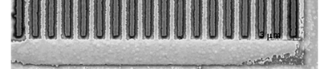
2 d. Mold fabrication: easily fabricated master molds in silicon via e-beam or focused ion beam (FIB) which can then be used to emboss multiple large area (> 12 mm/side) stamps/molds of superionic materials e. Mold life: over 80 replications have been demonstrated without loss of fidelity 7. Dimensional capabilities: moderate, < 100mm squared 8. Uniqueness: a. Only known direct patterning method for metals with nanoscale resolution b. Dry electrochemical process 9. Competition: Damascene 10. Limitations: a. Not suitable for multilayer situations b. Substrates limited now to chemistries tested 11. IP Status: Patents applied for 12. Potential Applications: a. Metamaterial structures b. Plasmonic structures and sensors (LSPR) c. Surface Enhanced Raman Spectroscopy (SERS) substrates (SERS enhancement > 10 6 ) d. Interdigitated electrodes: resistive and capacitive sensors e. Nano-wire sensors f. Chem-FETS g. Material tagging and bar-coding h. Metal enhanced Si etching i. Interconnects j. Miniature antenna 13. Current Research Focus: a. process scale-up and control b. New/different superionic materials 14. S4 Examples: a. Process: mold and etched S4 patterns:


3 b. S4 process fidelity demonstrated:


4 c. S4 produced nanoscale sensing patterns/arrays
5 Multifunctional Chemical Sensor Array

 allows for effective embossing of")


6 d. Effective embossing of nanopatterns for S4 process stamps A reduced Young s modulus and hardness for silver sulfide (~30 and o.5 GPa) allows for effective embossing of nanopatterns into stamps for the S4 process. Insert: space between the bow-tie pattern tips is 7 nm. Examples of metallic structures produced by the multiple-stamping/embossing approach. e. Flexible S4 ionic embossed stamps Flexible Stamp principle AFM image of pattern in Nafion polymer stamp.line width is <100 nm


7 f. New developments: Non-lithographic patterning of silicon, metal enhanced Si etching with S4 generated patterns. This process involves the use of S4 to create a pattern in a silver film that has been e-beam evaporated onto a silicon substrate that when placed in an etching solution of HF, H2O2, and EtOH, the silver catalyzes the selective etching of the silicon directly under the silver pattern. Illustration showing creation of silicon pillars/nanowires from silver S4 produced metal pattern which catalyzes HF etch process.
8 15. Recent Publications: a. Keng Hsu, Peter Schultz, Placid Ferreira, and Nicholas Fang, Electrochemical Nanoimprinting with Solid-State Superionic Stamps, Nano Letters, 2007, Vol. 7 No. 2, b. Keng Hsu, Peter Schultz, Placid Ferreira, and Nicholas X. Fang, Exploiting transport of guest metal ions in a host ionic crystal lattice for nanofabrication: Cu nanopatterning with Ag 2 S, Applied Physics A, Volume 97, Issue 4 (2009), Page 863 c. Keng Hsu, Ju H. Back, Moonsub Shim, Kin H. Fung, Placid Ferreira, and Nicholas Fang, SERS EM-field Enhancement Study through Fast Raman Mapping of Optical Sierpinski Carpet Fractals, Journal of Raman Spectroscopy, DOI: /jrs. 2581, 2010 d. Keng Hsu, Placid Ferreira, and Nicholas Fang, Numerical Modeling for the Dynamic Balance Between Interfacial Kinetics and Ionic Transport of Ag-Ag 2 S systems, Journal of Applied Physics, Submitted, 2010 e. Keng Hsu, Placid Ferreira, and Nicholas Fang, Controlled Directional Growth of Silver Micro Wires on a Solid Electrolyte Surface, Applied Physics Letters, 96, , 2010 f. Keng Hsu, Peter Schultz, Placid Ferreira, and Nicholas X. Fang, "Electrochemical Nanoimprinting of Silver and Copper with the Solid-State Superionic Stamping (S4) Process," Soft Lithography, John Rogers and Hong H. Lee (ed.), John Wiley and Sons, g. Winston Chern, Keng Hsu, Ik Su Chun, Bruno Pavanelli De Azeredo, Nick Fang, Placid Ferreira, and Xiuling Li, Non-Lithographic Patterning and Metal-Assisted Chemcial Etching for Manufacturing of Tunable Light-Emitting Silicon Nanowire Arrays, Nature Nanotech, submitted, 2009 h. S. Choi, M. Yan, I. Adesida, K. Hsu, and N. Fang, Ultradense gold nanostructures fabricated using hydrogen silsesquioxane resist and applications for surface-enhanced Raman spectroscopy, J. Vac. Sci. Technol. B 27 (6), 2009, i. Chaturvedi P., K. Hsu, S. Zhang, and N. X. Fang, "New Frontiers of Metamaterials: Design and Febrication," MRS Bulletin, 33:10, , 2008 j. Schultz P., Hsu, K., Fang, N., and, Ferreira, P., Solid-state electrochemical nanoimprinting of copper, Journal of Vacuum Science & Technology B: Microelectronics and Nanometer Structures -- November Volume 25, Issue 6, pp k. N. Fang, K. Hsu, K. Rapaka, and P. Ferreira, Pattern transfer by Solid-State Electrochemical Stamping, US patent application, No. 11/376,908. l. K. Jacobs, K. Hsu, N. Fang, P. Ferreira, "Direct Nanoscale Patterning of Metals Using Polymer Electrolytes," US patent application, No. TF07168-US m. X. Li, N. Fang, P. Ferreira, W. Chern, I. S. Chun, K. Hsu, Method of Forming an Array of High Aspect Ratio Semiconductor Nanostructures, No. TF09098-pro
Nanoimprinting in Polymers and Applications in Cell Studies. Albert F. YEE Chemical Engineering & Materials Science UC Irvine
 Nanoimprinting in Polymers and Applications in Cell Studies Albert F. YEE Chemical Engineering & Materials Science UC Irvine Presentation outline Motivation Reversal imprinting Soft inkpad imprinting on
NanoFabrication Systems DPN. Nanofabrication Systems. A complete line of instruments and tools for micro and nanopatterning applications
 DPN Nanofabrication Systems A complete line of instruments and tools for micro and nanopatterning applications DPN Nanofabrication Systems A complete line of instruments and tools for micro and nanopatterning
THIN METALLIC LAYERS STRUCTURED BY E-BEAM LITHOGRAPHY. Miroslav HORÁČEK, Vladimír KOLAŘÍK, Michal URBÁNEK, František MATĚJKA, Milan MATĚJKA
 THIN METALLIC LAYERS STRUCTURED BY E-BEAM LITHOGRAPHY Miroslav HORÁČEK, Vladimír KOLAŘÍK, Michal URBÁNEK, František MATĚJKA, Milan MATĚJKA Ústav přístrojové techniky AV ČR, v. v. i., Královopolská 147,
Fully-integrated, Bezel-less Transistor Arrays Using Reversibly Foldable Interconnects and Stretchable Origami Substrates
 Electronic Supplementary Material (ESI) for Nanoscale. This journal is The Royal Society of Chemistry 2016 Fully-integrated, Bezel-less Transistor Arrays Using Reversibly Foldable Interconnects and Stretchable
In-Situ Monitoring of Pattern Filling in Nano-Imprint Lithography Using Surface Plasmon Resonance
 Copyright 2011 American Scientific Publishers All rights reserved Printed in the United States of America Journal of Nanoscience and Nanotechnology Vol. 11, 1 6, 2011 In-Situ Monitoring of Pattern Filling
General Introduction to Microstructure Technology p. 1 What is Microstructure Technology? p. 1 From Microstructure Technology to Microsystems
 General Introduction to Microstructure Technology p. 1 What is Microstructure Technology? p. 1 From Microstructure Technology to Microsystems Technology p. 9 The Parallels to Microelectronics p. 15 The
Sub-5 nm Structures Process Development and Fabrication Over Large Areas
 A S Jugessur,, 2017, 1:1 SciFed Nanotech Research Letters Research Article Open Access Sub-5 nm Structures Process Development and Fabrication Over Large Areas * A S Jugessur * University of Iowa Microfabrication
Nanoscale Imaging, Material Removal and Deposition for Fabrication of Cutting-edge Semiconductor Devices
 Hitachi Review Vol. 65 (2016), No. 7 233 Featured Articles Nanoscale Imaging, Material Removal and Deposition for Fabrication of Cutting-edge Semiconductor Devices Ion-beam-based Photomask Defect Repair
Choi, Jun-Hyuk Korea Institute of Machinery & Materials
 The 11 th US-Korea Nanosymposium Choi, Jun-Hyuk 2014. 09. 29 Korea Institute of Machinery & Materials About KIMM Nano-research Bldg Clean RM Five Research Divisions; 1. Advanced Manufacturing Sys. 2. Extreme
Three-dimensional SU-8 structures by reversal UV imprint
 Three-dimensional SU-8 structures by reversal UV imprint W. Hu, a B. Yang, C. Peng, and S. W. Pang b Solid State Electronics Laboratory, Department of Electrical Engineering and Computer Science, The University
PARAMETER EFFECTS FOR THE GROWTH OF THIN POROUS ANODIC ALUMINUM OXIDES
 10.1149/1.2794473, The Electrochemical Society PARAMETER EFFECTS FOR THE GROWTH OF THIN POROUS ANODIC ALUMINUM OXIDES S. Yim a, C. Bonhôte b, J. Lille b, and T. Wu b a Dept. of Chem. and Mat. Engr., San
Advanced Polymers And Resists For Nanoimprint Lithography
 Q U A L I T Y A S S U R A N C E MICROSYSTEMS & NANOSYSTEMS SPECIAL REPORT Advanced Polymers And Resists For Nanoimprint Lithography Numerous polymer systems specifically designed for nanoimprint lithography
SCIENCE CHINA Technological Sciences. Replication of large area nanoimprint stamp with small critical dimension loss
 SCIENCE CHINA Technological Sciences RESEARCH PAPER March 2012 Vol.55 No.3: 600 605 doi: 10.1007/s11431-011-4695-3 Replication of large area nanoimprint stamp with small critical dimension loss MENG FanTao
Trench Structure Improvement of Thermo-Optic Waveguides
 International Journal of Applied Science and Engineering 2007. 5, 1: 1-5 Trench Structure Improvement of Thermo-Optic Waveguides Fang-Lin Chao * Chaoyang University of Technology, Wufong, Taichung County
A Functional Micro-Solid Oxide Fuel Cell with. Nanometer Freestanding Electrolyte
 Electronic Supplementary Material (ESI) for Journal of Materials Chemistry A. This journal is The Royal Society of Chemistry 2017 SUPPLEMENTARY INFORMATION A Functional Micro-Solid Oxide Fuel Cell with
Study of the resist deformation in nanoimprint lithography
 Study of the resist deformation in nanoimprint lithography Yoshihiko Hirai, a) Masaki Fujiwara, Takahiro Okuno, and Yoshio Tanaka Department of Mechanical System Engineering, Graduate School of Engineering,
Proton beam fabrication of nickel stamps for nanoimprint lithography
 Nuclear Instruments and Methods in Physics Research B 231 (2005) 407 412 www.elsevier.com/locate/nimb Proton beam fabrication of nickel stamps for nanoimprint lithography K. Ansari *, P.G. Shao, J.A. van
Today s Class. Materials for MEMS
 Lecture 2: VLSI-based Fabrication for MEMS: Fundamentals Prasanna S. Gandhi Assistant Professor, Department of Mechanical Engineering, Indian Institute of Technology, Bombay, Recap: Last Class What is
Title: Localized surface plasmon resonance of metal nanodot and nanowire arrays studied by far-field and near-field optical microscopy
 Contract Number: AOARD-06-4074 Principal Investigator: Heh-Nan Lin Address: Department of Materials Science and Engineering, National Tsing Hua University, 101, Sec. 2, Kuang Fu Rd., Hsinchu 30013, Taiwan
Micro and nano structuring of carbon based materials for micro injection moulding and hot embossing
 Micro and nano structuring of carbon based materials for micro injection moulding and hot embossing Victor Usov, Graham Cross, Neal O Hara, Declan Scanlan, Sander Paulen, Chris de Ruijter, Daniel Vlasveld,
Electrical Characterization of Tungsten Nanowires Deposited by Focused Ion Beam (FIB) *
 *") Nanopages 1 (2006) 2, 255 262 DOI: 10.1556/Nano.1.2006.2.10 Electrical Characterization of Tungsten Nanowires Deposited by Focused Ion Beam (FIB) * E. Horváth 1,2**, P. L. Neumann 2, A. L. Tóth 1, É. Vázsonyi
Nanopages 1 (2006) 2, 255 262 DOI: 10.1556/Nano.1.2006.2.10 Electrical Characterization of Tungsten Nanowires Deposited by Focused Ion Beam (FIB) * E. Horváth 1,2**, P. L. Neumann 2, A. L. Tóth 1, É. Vázsonyi
Supporting Information. Low Temperature Oxidation-free Selective Laser Sintering of Cu
 Supporting Information Low Temperature Oxidation-free Selective Laser Sintering of Cu Nanoparticle Paste on a Polymer Substrate for the Flexible Touch Panel Applications Jinhyeong Kwon 1,, Hyunmin Cho
Micromachining vs. Soft Fabrication
 Introduction to BioMEMS & Medical Microdevices Silicon Microfabrication Part 1 Companion lecture to the textbook: Fundamentals of BioMEMS and Medical Microdevices, by Prof., http://saliterman.umn.edu/
Module 13: Soft Lithography. Lecture 19: Soft Lithography 2
 Module 13: Soft Lithography Lecture 19: Soft Lithography 2 1 In the previous lecture we have introduced the concept of Soft Lithography and discussed three of the methods, which are Replica Molding, Micro
Introduction to Micro/Nano Fabrication Techniques. Date: 2015/05/22 Dr. Yi-Chung Tung. Fabrication of Nanomaterials
 Introduction to Micro/Nano Fabrication Techniques Date: 2015/05/22 Dr. Yi-Chung Tung Fabrication of Nanomaterials Top-Down Approach Begin with bulk materials that are reduced into nanoscale materials Ex:
Roll-to-Roll Nanoimprint - 6 회 -
 Roll-to-Roll Nanoimprint - 6 회 - 목차 Click to add Title 1 Roll to Roll nanoimprint Introduction : Continuous Production System (Roll-to-Roll) Fabrication Processes Fabrication of nano roll mold 2 Case study
Polymer Microfabrication (Part II) Prof. Tianhong Cui, Mechanical Engineering ME 8254
 Prof. Tianhong Cui, Mechanical Engineering ME 8254") Polymer Microfabrication (Part II) Prof. Tianhong Cui, Mechanical Engineering ME 8254 Other Polymer Techniques Embossing Low cost High throughput Structures as small as 25 nm Injection molding Features
Polymer Microfabrication (Part II) Prof. Tianhong Cui, Mechanical Engineering ME 8254 Other Polymer Techniques Embossing Low cost High throughput Structures as small as 25 nm Injection molding Features
High Performance Lithium Battery Anodes Using Silicon Nanowires
 Supporting Online Materials For High Performance Lithium Battery Anodes Using Silicon Nanowires Candace K. Chan, Hailin Peng, Gao Liu, Kevin McIlwrath, Xiao Feng Zhang, Robert A. Huggins and Yi Cui * *To
Scanning thermal microscopy probe capable of simultaneous electrical imaging and the addition of a diamond tip
 Scanning thermal microscopy probe capable of simultaneous electrical imaging and the addition of a diamond tip E Brown, L Hao, D C Cox and J C Gallop National Physical Laboratory, Hampton Road, Teddington,
Copper Interconnect Technology
 Tapan Gupta Copper Interconnect Technology i Springer Contents 1 Introduction 1 1.1 Trends and Challenges 2 1.2 Physical Limits and Search for New Materials 5 1.3 Challenges 6 1.4 Choice of Materials 7
Soft Lithography. Jin-Goo Park. Materials and Chemical Engineering Hanyang University, Ansan. Electronic Materials and Processing Lab.
 Hanyang University Soft Lithography Jin-Goo Park Materials and Chemical Engineering Hanyang University, Ansan Electronic Materials and Processing Lab. Introduction to Soft Lithography Research Micro- Electro-
Nanotechnology Principles, Applications, Careers, and Education. Copyright 2011 The Pennsylvania State University
 Nanotechnology Principles, Applications, Careers, and Education Copyright 2011 The Pennsylvania State University Outline What are the principles of nanotechnology? What are some applications? What kind
Surface Acoustic Wave fabrication using nanoimprint. Zachary J. Davis, Senior Consultant,
 Surface Acoustic Wave fabrication using nanoimprint Zachary J. Davis, Senior Consultant, zjd@teknologisk.dk Center for Microtechnology & Surface Analysis Micro and Nano Technology Sensor Technology Top
Vertically aligned Ni magnetic nanowires fabricated by diblock-copolymer-directed Al thin film anodization
 Vertically aligned Ni magnetic nanowires fabricated by diblock-copolymer-directed Al thin film anodization Researcher: Kunbae (Kevin) Noh, Graduate Student, MAE Dept. and CMRR Collaborators: Leon Chen,
3. Monodomain porous alumina obtained by nanoimprint lithography
 3. Monodomain porous alumina obtained by nanoimprint lithography 3.1 Nanoimprint lithography (NIL) In the previous chapter, the preparation of polydomain porous alumina by self-ordering was discussed.
Introduction to Nanofabrication: Top Down to Bottom Up
 Welcome to NACK s Webinar Introduction to Nanofabrication: Top Down to Bottom Up NACK is an NSF-funded ATE Resource Center supporting faculty in Nanotechnology Education Hosted by MATEC Networks www.matecnetworks.org
MEMSAND MICROSYSTEMS Design, Manufacture, and Nanoscale Engineering
 MEMSAND MICROSYSTEMS Design, Manufacture, and Nanoscale Engineering Second Edition TAI-RAN HSU Microsystems Design and Packaging Laboratory Department of Mechanical and Aerospace Engineering San Jose State
Large-area patterning by roller-based nanoimprint lithography
 JOANNEUM RESEARCH Forschungsgesellschaft Institute MATERIALS, Weiz, Austria Large-area patterning by roller-based nanoimprint lithography Ursula Palfinger, Dieter Nees, Stephan Ruttloff, Markus Leitgeb,
Surface plasmon dielectric waveguides
 Surface plasmon dielectric waveguides Igor I. Smolyaninov, Yu-Ju Hung, and Christopher C. Davis Department of Electrical and Computer Engineering, University of Maryland, College Park, MD 20742 Phone:
Lecture 22: Integrated circuit fabrication
 Lecture 22: Integrated circuit fabrication Contents 1 Introduction 1 2 Layering 4 3 Patterning 7 4 Doping 8 4.1 Thermal diffusion......................... 10 4.2 Ion implantation.........................
Thermal Nanoimprinting Basics
 Thermal Nanoimprinting Basics Nanoimprinting is a way to replicate nanoscale features on one surface into another, like stamping copies are made by traditional fabrication techniques (optical/ebeam lith)
We get small. Micron-scale Circuits and Structures from Prototype through Production
 We get small. Micron-scale Circuits and Structures from Prototype through Production Smaller, tighter, better. When you need to produce ultra-small electrical, mechanical and optical components to extreme
Large Area Functional Surfaces By Roll-to-Roll Nanoimprint Lithography Project: APPOLO
 Large Area Functional Surfaces By Roll-to-Roll Nanoimprint Lithography Project: APPOLO Mr. Theodoros Tachtsidis Nanotypos 23rd and 24th of June Amsterdam Core Overview Nanotypos is a pioneering research
Chapter 2 Capacitive Sensing Electrodes
 Chapter 2 Capacitive Sensing Electrodes The capacitive sensing electrodes on the top of a CMOS chip serve as an interface between the microelectronic readout system and the biological/chemical analyte.
CONTENTS. Introduction. NSOM Optical Fiber Probes
 CONTENTS Introduction NSOM Optical Fiber Probes AFM Probes AFM Probes Hard to achieve Force Constants and Resonance Frequencies Deep Trench AFM Probes Electrical and STM Probes Hollow AFM Nanopipette Probes
Thin. Smooth. Diamond.
 UNCD Wafers Thin. Smooth. Diamond. UNCD Wafers - A Family of Diamond Material UNCD is Advanced Diamond Technologies (ADT) brand name for a family of thin fi lm diamond products. UNCD Aqua The Aqua series
Fabrication of photonic band-gap crystals
 Fabrication of photonic band-gap crystals C. C. Cheng and A. Scherer California Institute of Technology, Pasadena, California 91125 Received 19 June 1995; accepted 9 August 1995 We describe the fabrication
Thin. Smooth. Diamond.
 UNCD Wafers Thin. Smooth. Diamond. UNCD Wafers - A Family of Diamond Material UNCD is Advanced Diamond Technologies (ADT) brand name for a family of thin fi lm diamond products. UNCD Aqua The Aqua series
Why Probes Look the Way They Do Concepts and Technologies of AFM Probes Manufacturing
 Agilent Technologies AFM e-seminar: Understanding and Choosing the Correct Cantilever for Your Application Oliver Krause NanoWorld Services GmbH All mentioned company names and trademarks are property
Epitaxy and Roughness Study of Glancing Angle Deposited Nanoarrays. Hamid Alouach and G. J. Mankey
 Epitaxy and Roughness Study of Glancing Angle Deposited Nanoarrays Hamid Alouach and G. J. Mankey Introduction Objective: Approach: Characterization: Fabrication of nanoscale magnetic wires for spin transport
Silver Diffusion Bonding and Layer Transfer of Lithium Niobate to Silicon
 Chapter 5 Silver Diffusion Bonding and Layer Transfer of Lithium Niobate to Silicon 5.1 Introduction In this chapter, we discuss a method of metallic bonding between two deposited silver layers. A diffusion
Local Oxide Growth Mechanisms on Nickel Films
 Materials Transactions, Vol. 48, No. 3 (2007) pp. 471 to 475 #2007 The Japan Institute of Metals Local Oxide Growth Mechanisms on Nickel Films Te-Hua Fang* 1 and Kuan-Jen Chen* 2 Institute of Mechanical
Nanyang Technological University School of Materials Science & Engineering
 Final Year Project Proposal 1 3D Assembly of Nano/Micro Zirconia Particles for Enhanced Energy Damping Capacity Dr Du Zehui (duzehui@ntu.edu.sg) To develop the best possible method to assemble micro/nano-scale
Developing Enhanced Substrates for OLED SSL
 Developing Enhanced Substrates for OLED SSL DOE SSL R&D Manufacturing Workshop San Diego CA 7 May, 2014 Dr. W. Dennis Slafer MicroContinuum, Inc. 57 Smith Place Cambridge, MA 02138 www.microcontinuum.com
Plasmonics using Metal Nanoparticles. Tammy K. Lee and Parama Pal ECE 580 Nano-Electro-Opto-Bio
 Plasmonics using Metal Nanoparticles Tammy K. Lee and Parama Pal ECE 580 Nano-Electro-Opto-Bio April 1, 2007 Motivation Why study plasmonics? Miniaturization of optics and photonics to subwavelength scales
FABRICATION ENGINEERING MICRO- NANOSCALE ATTHE AND. Fourth Edition STEPHEN A. CAMPBELL. of Minnesota. University OXFORD UNIVERSITY PRESS
 AND FABRICATION ENGINEERING ATTHE MICRO- NANOSCALE Fourth Edition STEPHEN A. CAMPBELL University of Minnesota New York Oxford OXFORD UNIVERSITY PRESS CONTENTS Preface xiii prrt i OVERVIEW AND MATERIALS
Microelectronics. Integrated circuits. Introduction to the IC technology M.Rencz 11 September, Expected decrease in line width
 Microelectronics Introduction to the IC technology M.Rencz 11 September, 2002 9/16/02 1/37 Integrated circuits Development is controlled by the roadmaps. Self-fulfilling predictions for the tendencies
Direct Patterning of Self Assembled Nano-Structures of Block Copolymers via Electron Beam Lithography
 Macromolecular Research, Vol. 13, No. 5, pp 435-440 (2005) Direct Patterning of Self Assembled Nano-Structures of Block Copolymers via Electron Beam Lithography Bo Kyung Yoon, Wonseok Hwang, Youn Jung
ADVANCED MANUFACTURING CHOICES: TOWARDS A CARBON WORLD. ENG Spring 2017, Class 10, Carbon-MEMS/Carbon-NEMS
 ADVANCED MANUFACTURING CHOICES: TOWARDS A CARBON WORLD ENG 165-265 Spring 2017, Class 10, Carbon-MEMS/Carbon-NEMS Table of Content Why carbon? Carbon MEMS and Carbon NEMS: A New Way of Manufacturing Carbon
Mater. Res. Soc. Symp. Proc. Vol Materials Research Society
 Mater. Res. Soc. Symp. Proc. Vol. 940 2006 Materials Research Society 0940-P13-12 A Novel Fabrication Technique for Developing Metal Nanodroplet Arrays Christopher Edgar, Chad Johns, and M. Saif Islam
WP7 JRA2 JRA2 Research on High Precision Manufacturing. Investigation of optimum NIL stamp fabrication method to copy sub-10 nm BCP features
 DELIVERABLE REPORT WP7 JRA2 JRA2 Research on High Precision Manufacturing D7.1 Investigation of optimum NIL stamp fabrication method to copy sub-10 nm BCP features M18 NFFA-Europe has received funding
Chapter 3 Silicon Device Fabrication Technology
 Chapter 3 Silicon Device Fabrication Technology Over 10 15 transistors (or 100,000 for every person in the world) are manufactured every year. VLSI (Very Large Scale Integration) ULSI (Ultra Large Scale
Micro-Nano Fabrication Research
 Micro-Nano Fabrication Research Technical Education Quality Improvement Programme 22-23 December 2014 Dr. Rakesh G. Mote Assistant Professor Department of Mechanical Engineering IIT Bombay rakesh.mote@iitb.ac.in;
NO x gas response characteristics of thin film mixed oxide semiconductor
 Sensors and Actuators B 108 (2005) 211 215 NO x gas response characteristics of thin film mixed oxide semiconductor Kap-Duk Song a, Jung-Il Bang a, Sang-Rok Lee a, Yun-Su Lee a, Young-Ho Hong b, Duk-Dong
1 MARCH 2017 FILM DEPOSITION NANOTECHNOLOGY
 1 MARCH 2017 FILM DEPOSITION NANOTECHNOLOGY PRESENTATION Pedro C. Feijoo E-mail: PedroCarlos.Feijoo@uab.cat FABRICATION TECHNOLOGIES FOR NANOELECTRONIC DEVICES. PEDRO C. FEIJOO 2 FILM GROWTH Chemical vapor
Nanoimprint of a 3D structure on an optical fiber for light wavefront manipulation
 Nanoimprint of a 3D structure on an optical fiber for light wavefront manipulation Giuseppe Calafiore,1, Alexander Koshelev,1, Frances I. Allen 2,3, Scott Dhuey 3, Simone Sassolini 3, Edward Wong 3, Paul
Note Application of Screen Printing in Flexible Miniature Thermocouple Process Development
 Int. J. Electrochem. Sci., 10 (2015) 3082-3087 Note Application of Screen Printing in Flexible Miniature Thermocouple Process Development International Journal of ELECTROCHEMICAL SCIENCE www.electrochemsci.org
Conductive glass (NTA glass )
") Art Beam Co. Ltd. Conductive glass (NTA glass ) Nano Technology Assorted Glass Japanese Patent No. 3854985 (applied for 2001, granted 2006) Vanadate glass and its manufacturing method Patent holder: Tetsuaki
Art Beam Co. Ltd. Conductive glass (NTA glass ) Nano Technology Assorted Glass Japanese Patent No. 3854985 (applied for 2001, granted 2006) Vanadate glass and its manufacturing method Patent holder: Tetsuaki
Chapter 7 NANOIMPRINTED CIRCULAR GRATING DISTRIBUTED FEEDBACK DYE LASER
 Chapter 7 66 NANOIMPRINTED CIRCULAR GRATING DISTRIBUTED FEEDBACK DYE LASER 7.1 Introduction In recent years, polymer dye lasers have attracted much attention due to their low-cost processing, wide choice
Outline. Introduction to the LIGA Microfabrication Process. What is LIGA? The LIGA Process. Dr. Bruce K. Gale Fundamentals of Microfabrication
 Outline Introduction to the LIGA Microfabrication Process Dr. Bruce K. Gale Fundamentals of Microfabrication What is LIGA? The LIGA Process Lithography Techniques Electroforming Mold Fabrication Analyzing
Metallization deposition and etching. Material mainly taken from Campbell, UCCS
 Metallization deposition and etching Material mainly taken from Campbell, UCCS Application Metallization is back-end processing Metals used are aluminum and copper Mainly involves deposition and etching,
Figure 6. Rare-gas atom-beam diffraction patterns. These results were obtained by Wieland Schöllkopf and Peter Toennies at the Max-Planck Institute
 Figure 6. Rare-gas atom-beam diffraction patterns. These results were obtained by Wieland Schöllkopf and Peter Toennies at the Max-Planck Institute in Göttingen, Germany, using a freestanding, 100nm-period
Applications of Nano Patterning Process 1. Patterned Media
 Applications of Nano Patterning Process 1. Patterned Media Contents Introduction Part. 1. Nanoimprinting on Glass Substrate for Patterned Media Part. 2. Nanoinjection Molding of Nanopillars for Patterned
MODERN COMPUTER TENDING TOWARDS NANOTECHNOLOGY MAKING GRATE GROWTH IN 21 ST CENTURY
 MODERN COMPUTER TENDING TOWARDS NANOTECHNOLOGY MAKING GRATE GROWTH IN 21 ST CENTURY Mrs. Jayashree Yadannavar Department of Information Technology,MIT AOE, Alandi(D),Pune ABSTRACT At present in the field
Supplementary Figure S1 Photograph of MoS 2 and WS 2 flakes exfoliated by different metal naphthalenide (metal = Na, K, Li), and dispersed in water.
, and dispersed in water.") Supplementary Figure S1 Photograph of MoS 2 and WS 2 flakes exfoliated by different metal naphthalenide (metal = Na, K, Li), and dispersed in water. Supplementary Figure S2 AFM measurement of typical LTMDs
Supplementary Figure S1 Photograph of MoS 2 and WS 2 flakes exfoliated by different metal naphthalenide (metal = Na, K, Li), and dispersed in water. Supplementary Figure S2 AFM measurement of typical LTMDs
for Bioanalytical Applications
 Conferinţa Diaspora in Cercetarea Ştiinţifică şi Invăţămantul Superior din Romania Bucuresti, 21-24 Septembrie 2010 Multifunctional Plasmonic Nanosensors for Bioanalytical Applications Simion Astilean
Gas and surface applications of atmospheric pressure plasmas
 Gas and surface applications of atmospheric pressure plasmas Eugen Stamate Technical University of Denmark Roskilde 4000, Denmark OUTLINE Introduction of DTU Energy Conversion and Storage Activities in
Flexible Substrates for Smart Sensor Applications
 Flexible Substrates for Smart Sensor Applications A novel approach that delivers miniaturized, hermetic, biostable and highly reliable smart sensor modules. AUTHORS Dr. Eckardt Bihler, Dr. Marc Hauer,
Imprint lithography for curved cross-sectional structure using replicated Ni mold
 Imprint lithography for curved cross-sectional structure using replicated Ni mold Yoshihiko Hirai, a) Satoshi Harada, Hisao Kikuta, and Yoshio Tanaka Mechanical System Engineering, Graduate School of Engineering,
During solution evaporation, there are two major competing evaporation-driven effects, coffee ring effect and Marangoni flow.
 Abstract Evaporation driven particle packing has been investigated to reveal interesting patterns at micrometer to millimeter scale. While the microscopic structures of these patterns are well characterized,
FY06 ACCOMPLISHMENTS. Nanoelectronics Manufacture, Inspection, and Repair using Thermal Dip Pen Nanolithography
 FY06 ACCOMPLISHMENTS Nanoelectronics Manufacture, Inspection, and Repair using Thermal Dip Pen Nanolithography William P. King Georiga Institute of Technology FY06 was the second year of this grant, and
Holographix LLC Overview. High quality custom replicated optics and surface relief patterns in production volumes
 Holographix LLC Overview 2018 High quality custom replicated optics and surface relief patterns in production volumes One location in Marlborough, MA. 15,000 sq. ft. facility with additional space available
ScienceDirect. Growth of Carbon Nano Tubes on Copper Substrate Suitable for Lithium Ion Battery Anode
 Available online at www.sciencedirect.com ScienceDirect Procedia Materials Science 11 (2015 ) 634 638 5th International Biennial Conference on Ultrafine Grained and Nanostructured Materials, UFGNSM15 Growth
Integration of Block-Copolymer with Nano- Imprint Lithography: Pushing the Boundaries of Emerging Nano-Patterning Technology
 Integration of Block-Copolymer with Nano- Imprint Lithography: Pushing the Boundaries of Emerging Nano-Patterning Technology April 2010 update SNL Geoff Brennecka (PI) Bruce Burckel Matt George Jack Skinner
Simple UV-based Soft-lithography Process for. Fabrication of Low-Loss Polymer PSQ-L-based. Waveguides
 Simple UV-based Soft-lithography Process for Fabrication of Low-Loss Polymer PSQ-L-based Waveguides Jie Teng 1, 2, 4, Stijn Scheerlinck 4, Geert Morthier 4, Roel Baets 4, Hongbo Zhang 2,3, Xigao Jian 2,3,
High Definition Selective Metallization for Printed Electronics
 High Definition Selective Metallization for Printed Electronics Wolfgang Decker VAST FILMS, Ltd. Outline Introduction of VAST FILMS What is Selective Metalization Range of Applications for Selective Metalization
UT Austin, ECE Department VLSI Design 2. CMOS Fabrication, Layout Rules
 2. CMOS Fabrication, Layout, Design Rules Last module: Introduction to the course How a transistor works CMOS transistors This module: CMOS Fabrication Design Rules CMOS Fabrication CMOS transistors are
Change in stoichiometry
 Measurement of Gas Sensor Performance Gas sensing materials: 1. Sputtered ZnO film (150 nm (Massachusetts Institute of Technology) 2. Sputtered SnO 2 film (60 nm) (Fraunhofer Institute of Physical Measurement
Manufacturing Technologies for MEMS and SMART SENSORS
 4 Manufacturing Technologies for MEMS and SMART SENSORS Dr. H. K. Verma Distinguished Professor (EEE) Sharda University, Greater Noida (Formerly: Deputy Director and Professor of Instrumentation Indian
Czochralski Crystal Growth
 Czochralski Crystal Growth Crystal Pulling Crystal Ingots Shaping and Polishing 300 mm wafer 1 2 Advantage of larger diameter wafers Wafer area larger Chip area larger 3 4 Large-Diameter Wafer Handling
SOLAR ENERGY. Approximately 120,000 TW of solar energy strikes the earth s surface, capturing only a fraction could supply all of our energy needs.
 SOLAR ENERGY Approximately 120,000 TW of solar energy strikes the earth s surface, capturing only a fraction could supply all of our energy needs. What is Photovoltaics? Photovoltaics is a high-technology
Production and analysis of optical gratings and nanostructures created by laser based methods
 Summary of the Ph.D. thesis Production and analysis of optical gratings and nanostructures created by laser based methods Kiss Bálint Supervisor: Dr. Vass Csaba Research fellow Doctoral School in Physics
Free standing Multilayer Thin Film of Cellulose Nanocrystals
 Free standing Multilayer Thin Film of Cellulose Nanocrystals Chaoyang Jiang Department of Chemistry The University of South Dakota Edmonton, June 25, 2009 Cellulose Nanocrystals Nanotechnology R&D Priority
Preprint - Mechatronics 2008, Le Grand-Bornand, France, May
 Potentialities of piezoresistive cantilever force sensors based on free standing thick films Hélène Debéda(*), Isabelle Dufour, Patrick Ginet, Claude Lucat University of Bordeaux 1, IMS Laboratory, 51
Fabrication characteristics of a line-and-space pattern and a dot pattern on a roll mold by using electron-beam lithography
 0123456789 Bulletin of the JSME Journal of Advanced Mechanical Design, Systems, and Manufacturing Vol.10, No.5, 2016 Fabrication characteristics of a line-and-space pattern and a dot pattern on a roll
Metallic Antireflection Structures Made from Silver Ink by a Liquid Transfer Imprint Lithography Technique
 Journal of Photopolymer Science and Technology Volume 30, Number 5 (2017) 539-544 C 2017SPST Metallic Antireflection Structures Made from Silver Ink by a Liquid Transfer Imprint Lithography Technique Ichiro
纳米压印技术最新进展. Obducat Technologies AB., Sweden Gang Luo,
 纳米压印技术最新进展 Obducat Technologies AB., Sweden Gang Luo, 20170711 History 2016 Launch of SINDRE Large Area 2015 Acquire Solarsemi Gmbh 2015 Awarded by NNT for Pioneering NIL into production 2014 Launch and
Bio MEMS Class -1 st week
 Bio MEMS Class -1 st week Jang, Jaesung Ref: Bashir ADDR Review paper, 2004. 1 Introduction Bio-MEMS: devices or systems, constructed using techniques inspired from micro/nano-scale fabrication, that are
Chemical Mechanical Planarization
 1 Chemical Mechanical Planarization SFR Workshop & Review November 14, 2002 David Dornfeld, Fiona Doyle, Costas Spanos, Jan Talbot Berkeley, CA 2 Focus of this presentation CMP research milestones in SFR
Pattern Formation in PMMA Film Induced by Electric Field
 Pattern Formation in PMMA Film Induced by Electric Field OLEKSIY LYUTAKOV, 1 IVAN HÜTTEL, 1 VÁCLAV PRAJZLER, 2 VÍTĚZSLAV JEŘÁBEK, 2 ALEXANDER JANČÁREK, 3 VLADIMÍR HNATOWICZ, 4 VÁCLAV ŠVORČÍK 1 1 Department