Introduction Sample deposition system Cavity deposition system prototype Surface characterization Beyond niobium
|
|
|
- Curtis Owen
- 5 years ago
- Views:
Transcription
1 Genfa Wu Introduction Sample deposition system Cavity deposition system prototype Surface characterization Beyond niobium 1
2 United We Stand Succeed JLAB ECR thin film collaboration: JLAB: L. Phillips, R. Rimmer, A-M. Valente, H. Wang, A. Wu, G. Wu Cornell: H. Padamsee (LEPP), L. Hand (Physics) College of William and Mary: M. Kelley SANDIA: T. Renk Black Laboratory: R. Crooks 2
3 a glow discharge can be established using only metal vapor but the discharge is very unstable and this method is generally not practical. -- R. F. Bunshah, et., al., Deposition Technologies for Films and Coatings 3

4 Energetic deposition process Movchan-Demchishin Zone Model (MDT) An illustration of approximate deposition energy is shown in above figure. Different materials will have different energy ranges. J. A. Thornton, JVST, Vol. 11, No. 4, (1974) p666 4


5 The illustration of the energetic vacuum deposition by ECR plasma 5
![Cavity deposition prototype 1200 1100 1000 B field [gauss] 900 800 700 600 0.0 0.5 1.0 1.5 2.0 Z Axis [in] 2.5 3.0 0.0 1.5 1.0 0.5 3.0 2.5 2.0 R Axis [in] Sample deposition system 7.](/docs-images/90/102864560/images/6-1.jpg "5kW hearth, 130 A/s 1200 1100 1000 B field [gauss] 900 800 700 600 0.0 0.5 1.0 1.5 2.0 Z Axis [in] 2.5 3.0 0.0 1.5 1.0 0.5 R Axis [in] 3.0 2.5 2.0 Cavity deposition system 15 kw Rod-fed, 100 A/s 6")
6 Cavity deposition prototype B field [gauss] Z Axis [in] R Axis [in] Sample deposition system 7.5kW hearth, 130 A/s B field [gauss] Z Axis [in] R Axis [in] Cavity deposition system 15 kw Rod-fed, 100 A/s 6
 9000 l/s cryopump system (3) bucking coil for E-gun (4) top and bottom iron yokes (outer")
 T vacuum chamber (10) top coil (11) Cu cavity (12) bottom coil.")
7 Cavity deposition prototype System design of the Nb thin film coating on a 500MHz Cu cavity (1) 14kW rod-fed E-gun (2) 9000 l/s cryopump system (3) bucking coil for E-gun (4) top and bottom iron yokes (outer iron shield is removed for illustration) (5) center coils (6) Nb grid tube (7) bias insulator (8) WR284 waveguide E-bend and horn to the grid tube (9) T vacuum chamber (10) top coil (11) Cu cavity (12) bottom coil

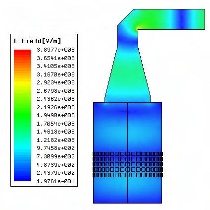
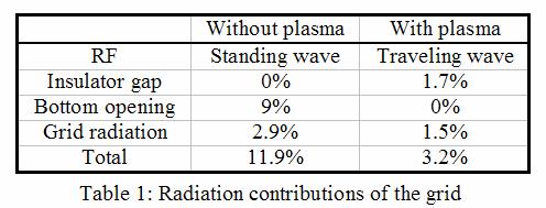
8 RF radiation 8


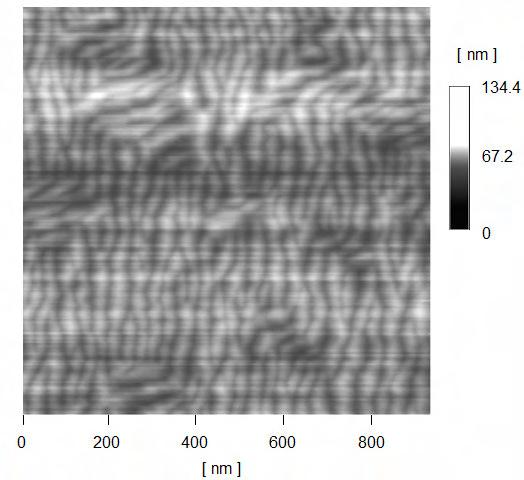
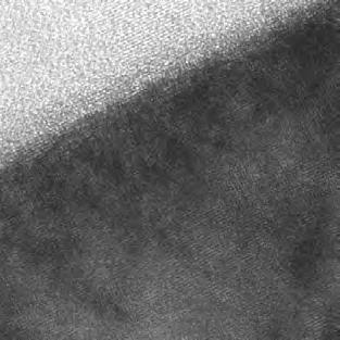
9 Optical image of copper surface Mechanical polished 100 µm chemical polished 120 µm Electropolished 15 µm after chemical etching Surface from BCP/EP was wavy Time consuming for Mech/EP 9


10 Low temperature Characterization Function Generator SC thin film 100 Ω 20MΩ Lock-in Amplifier A C D B THIN FILM SAMPLE 10
11 Transition temperature and RRR T r a n s i t i o n W i d t h T [ K ] T T S u b s t r a t e b i a s v o l t a g e [ V ] T r a n s i t i o n T e m p e r a t u r e T [ K ] T r a n s i t i o n W i d t h T [ K ] T T S u b s t r a t e b i a s v o l t a g e [ V ] Bias voltage effect on transition temperature and transition width, measured by an inductive method. Substrate is A-cut sapphire (left), Substrate is electropolished copper (right) T r a n s i t i o n T e m p e r a t u r e T [ K ] R R R F i l m t h i c k n e s s [ n m ] T c = (T 90% + T 10% )/2 T c = (T 90% - T 10% )/2 11

12 Film characterizations SEM X-ray diffraction AFM Nb/Cu-90 Film RMS=94 nm, profilometer SIMS TEM 12
13 Summary of thin film sample Niobium Ion Energy is around 63 ev without bias voltage, and controllable. Cryogenically, the process achieves a reasonably high RRR niobium thin film with excellent superconducting transition temperature and width. RRR appears to be more closely related to the film thickness than to the deposition energy. Epitaxial growth of niobium on sapphire has been achieved. The substrate bias voltage of -60 V is believed to be the preferred value based on the transition width, the crystal orientation spread, and the AFM results. For a copper substrate, a better film quality likely requires higher deposition energy than sahhpire substrate, which needs further studies. 13
14 Summary of thin film sample (cont.) based on SIMS analysis Nb-Cu sample surfaces are smooth locally Nb-Cu surfaces may have much less hydrocarbons and other residuals or contaminants as compared with those on the Nb surfaces obtained conventionally (BCP or EP). Nb-Cu samples appear to have more oxygen on the surfaces and oxygen penetrates deeper into the interior of the samples. This may be resulted from the residual gases in the deposition chamber and from the fact that the grain size of Nb-Cu is small. 14
15 Beyond niobium, Material, we will look at: NbN, NbTiN, Nb3Sn, MgB2 Process we can setup: (Bias) Sputtering, Plasma, PLD. Collaboration process: Vacuum Arc, pulsed ion ablation Low power application: 4k medium performance for university or hospital operation. High power application: 4K high performance for compact, high power FEL 15
ENERGETIC DEPOSITION IN VACUUM
 ENERGETIC DEPOSITION IN VACUUM G. Wu, Virginia Tech, Blacksburg, VA 24061,USA L. Phillips, R. Sundelin, T. Goodman, JLAB*, Newport News, VA 23606, USA Abstract In hoping to improve Niobium deposition on
Nb/Cu, Nb 3 Sn/Cu Thin Film Cavity
 Nb/Cu, Nb 3 Sn/Cu Thin Film Cavity Genfa Wu Abstract A thin film deposition method inside an elliptical cavity is proposed. The system uses the substrate copper cavity as the vacuum chamber. The ECR plasma
RF AND STRUCTURAL CHARACTERIZATION OF NEW SRF FILMS *
 RF AND STRUCTURAL CHARACTERIZATION OF NEW SRF FILMS * A.-M. Valente-Feliciano #, H.L. Phillips, C.E. Reece, and X. Zhao, Thomas Jefferson National Accelerator Facility, Newport News, VA, U.S.A. D. Gu,
Deposition of niobium and other superconducting materials with high power impulse magnetron sputtering: Concept and first results
 15th International Conference on RF Superconductivity July 25-29, 2011, Chicago Deposition of niobium and other superconducting materials with high power impulse magnetron sputtering: Concept and first
Electron Microscopy Studies of Niobium Thin Films on Copper
 Electron Microscopy Studies of Niobium Thin Films on Copper Roy Crooks 1, Greg Thompson 2, Robb Morris 2, Michelle Adams Hughes 3, Daudi Waryoba 3, and Peter Kalu 3 1 Black Laboratories, L.L.C., Newport
Status of Research on Deposition of Superconducting Films for RF Accelerating Cavities
 Status of Research on Deposition of Superconducting Films for RF Accelerating Cavities J. Langner, L. Catani*, A. Cianchi*, K. Czaus, R. Mirowski, R. Russo*, M.J. Sadowski, S. Tazzari*, F. Tazzioli***,
Review of RF properties of NbN and MgB 2 thin coating on Nb samples and cavities
 Review of RF properties of NbN and MgB 2 thin coating on Nb samples and cavities Grigory Eremeev Mechanical Design and Engineering Group Accelerator Operations and Technology Division Los Alamos National
REVIEW ON Q-DROP MECHANISMS
 REVIEW ON Q-DROP MECHANISMS Bernard VISENTIN # CEA-Saclay, DSM / DAPNIA / SACM - 91191 Gif / Yvette Cedex France Abstract Manufacturing of radiofrequency cavities by deposition of superconducting thin
Plasma cleaning: A new possible treatment for niobium. superconducting cavity after nitrogen doping
 1 Plasma cleaning: A new possible treatment for niobium superconducting cavity after nitrogen doping Ziqin Yang 1, Xiangyang Lu 1), Datao Xie 1, Lin Lin 1, Kui Zhou 2, Jifei Zhao 1, Deyu Yang 1, Weiwei
Thin Films: Sputtering Systems (Jaeger Ch 6 & Ruska Ch 7,) Can deposit any material on any substrate (in principal) Start with pumping down to high
 Can deposit any material on any substrate (in principal) Start with pumping down to high") Thin Films: Sputtering Systems (Jaeger Ch 6 & Ruska Ch 7,) Can deposit any material on any substrate (in principal) Start with pumping down to high vacuum ~10-7 torr Removes residual gases eg oxygen from
Thin Films: Sputtering Systems (Jaeger Ch 6 & Ruska Ch 7,) Can deposit any material on any substrate (in principal) Start with pumping down to high vacuum ~10-7 torr Removes residual gases eg oxygen from
Progress in Use of Ultra-High Vacuum Cathodic Arcs for Deposition of Thin Film Superconducting Layers
 SRF Progress in Use of Ultra-High Vacuum Cathodic Arcs for Deposition of Thin Film Superconducting Layers J. Langner 1, M.J. Sadowski 1, P. Strzyzewski 1, R. Mirowski 1, J. Witkowski 1, S. Tazzari 2, L.
Construction of an innovative cylindrical magnetron sputtering source for HIE- ISOLDE superconductive Nb/Cu QWRs
 ISTITUTO NAZIONALE DI FISICA NUCLEARE LABORATORI DI SUPERCONDUCTIVITA UNIVERSITY OF FERRARA DEPARTMENT OF PHYSICS Technologies for accelerator and targets in nuclear physics Construction of an innovative
Overview of Advanced Surface Science activities at CERN. S.Calatroni, M.Taborelli TE-VSC-SCC
 Overview of Advanced Surface Science activities at CERN S.Calatroni, M.Taborelli TE-VSC-SCC Basic components of particle accelerators Technology Department 10 October 2014 S. Calatroni & M. Taborelli 2
DC magnetism of Niobium thin films
 Loughborough University Institutional Repository DC magnetism of Niobium thin films This item was submitted to Loughborough University's Institutional Repository by the/an author. Citation: WILDE, S....et
TOPOGRAPHY AND ELECTRICAL PROPERTIES OF SPUTTERED NIOBIUM FILMS
 TOPOGRAPHY AND ELECTRICAL PROPERTIES OF SPUTTERED NIOBIUM FILMS L. van Loyen 1*, D. Elefant 1, V. Palmieri 2, W. Venturini D. 2, J. Halbritter 3 1 Institute of Solid State and Materials Research Dresden,
Metallization deposition and etching. Material mainly taken from Campbell, UCCS
 Metallization deposition and etching Material mainly taken from Campbell, UCCS Application Metallization is back-end processing Metals used are aluminum and copper Mainly involves deposition and etching,
Growth Of TiO 2 Films By RF Magnetron Sputtering Studies On The Structural And Optical Properties
 Journal of Multidisciplinary Engineering Science and Technology (JMEST) Growth Of TiO 2 Films By RF Magnetron Sputtering Studies On The Structural And Optical Properties Ahmed K. Abbas 1, Mohammed K. Khalaf
Thin Film Characterizations Using XRD The Cases of VO2 and NbTiN
 Thin Film Characterizations Using XRD The Cases of VO2 and NbTiN A thesis submitted in partial fulfillment of the requirement for the degree of Bachelor of Arts / Science in Physics from The College of
Pushing SRF Into the Future Materials and Processes R&D
 Pushing SRF Into the Future Materials and Processes R&D Charles Reece It is not yet clear what surface properties are the most important for achieving high Q and high peak RF fields. The answer to this
Linear Plasma Sources for Surface Modification and Deposition for Large Area Coating
 Linear Plasma Sources for Surface Modification and Deposition for Large Area Coating Dr Tony Williams Gencoa Ltd, UK Victor Bellido-Gonzalez, Dr Dermot Monaghan, Dr Joseph Brindley, Robert Brown SVC 2016,
Formation mechanism of new corrosion resistance magnesium thin films by PVD method
 Surface and Coatings Technology 169 170 (2003) 670 674 Formation mechanism of new corrosion resistance magnesium thin films by PVD method a, a a a b M.H. Lee *, I.Y. Bae, K.J. Kim, K.M. Moon, T. Oki a
Thin Films: Sputtering Systems (Jaeger Ch 6 & Ruska Ch 7,) Sputtering: gas plasma transfers atoms from target to substrate Can deposit any material
 Sputtering: gas plasma transfers atoms from target to substrate Can deposit any material") Thin Films: Sputtering Systems (Jaeger Ch 6 & Ruska Ch 7,) Sputtering: gas plasma transfers atoms from target to substrate Can deposit any material on any substrate (in principal) Start with pumping down
Thin Films: Sputtering Systems (Jaeger Ch 6 & Ruska Ch 7,) Sputtering: gas plasma transfers atoms from target to substrate Can deposit any material on any substrate (in principal) Start with pumping down
II. NEG THIN FILM DEPOSITION
 Deposition of Non-Evaporable Getter Thin Films and Vacuum Pumping Performances Ankit Sur Engineering Department, Wayne State University, Detroit, MI 48202 The ERL (Energy Recovery Linac) proposed at Cornell
Solar Selective Absorber Coating Methods Plasma Processes
 Solar Selective Absorber Coating Methods Plasma Processes Paul Gantenbein & Elimar Frank SPF - Institut für Solartechnik University of Applied Sciences Rapperswil (HSR) Optical properties of a selective
Previous Lecture. Vacuum & Plasma systems for. Dry etching
 Previous Lecture Vacuum & Plasma systems for Dry etching Lecture 9: Evaporation & sputtering Objectives From this evaporation lecture you will learn: Evaporator system layout & parts Vapor pressure Crucible
RBS AND NRS ANALYSIS OF SPUTTERED NB FILMS ANNEALED AT DIFFERENT TEMPERATURES
 RBS AND NRS ANALYSIS OF SPUTTERED NB FILMS ANNEALED AT DIFFERENT TEMPERATURES M.RIBEAUDEAU, P.BOSLAND Service d'etude des Accélérateurs, CEA/SACLAY, F-91 191 Gif-sur-Yvette A.CHEVARIER, O.GUISE, P.TROUVE
MgB 2 for SRF Cavities
 MgB 2 for SRF Cavities Tsuyoshi Tajima Los Alamos Neutron Science Center Los Alamos National Laboratory LA-UR-05-5049rev TFSRF 2005, JLAB, July 17-18, 2005 1 Why do we need to look for new SC materials
IBS/e Ion Beam Sputter Deposition and Etching System. IBS/e with KDC-10 Ion Beam Sputter Deposition and Etching System with Kaufman Ion Source
 IBS/e Ion Beam Sputter Deposition and Etching System IBS/e with KDC-10 Ion Beam Sputter Deposition and Etching System with Kaufman Ion Source The Model IBS/e is a high vacuum thin film deposition system
QUANTUM EFFICIENCY MEASUREMENTS OF Mg FILMS PRODUCED BY PULSED LASER ABLATION DEPOSITION FOR HIGH BRIGHTNESS ELECTRON SOURCES*
 QUANTUM EFFICIENCY MEASUREMENTS OF Mg FILMS PRODUCED BY PULSED LASER ABLATION DEPOSITION FOR HIGH BRIGHTNESS ELECTRON SOURCES* G.Gatti, L.Cultrera, F.Tazzioli, C.Vicario INFN-LNF A.Fiori University of
Roman Chistyakov and Bassam Abraham Zond Inc/Zpulser LLC, Mansfield, MA
 HIPIMS Arc-Free Reactive Sputtering of Non-conductive Films Using the ENDURA 200 mm Cluster Tool: Direct Comparison Between Pulsed DC Pinnacle Plus and HIPIMS Cyprium Roman Chistyakov and Bassam Abraham
Mass Production of Clear Barriers. Requirements on Vacuum Web Coaters for Quality Assurance. Rainer Ludwig, Applied Films, Alzenau, Germany.
 Mass Production of Clear Barriers Requirements on Vacuum Web Coaters for Quality Assurance Rainer Ludwig, Applied Films, Alzenau, Germany Abstract An increasing number of packages using Transparent Barrier
Vacuum deposition of TiN
 J.Lorkiewicz DESY.27.10.02 Vacuum deposition of TiN (TiN coating of high power coupler elements as an anti-multipactor remedy at DESY) The scope of the project: - reducing secondary electron emission and
Supporting Online Material for
 www.sciencemag.org/cgi/content/full/327/5961/60/dc1 Supporting Online Material for Polarization-Induced Hole Doping in Wide Band-Gap Uniaxial Semiconductor Heterostructures John Simon, Vladimir Protasenko,
BEHAVIOUR OF GAS CONDITIONS DURING VACUUM ARC DISCHARGES USED FOR DEPOSITION OF THIN FILMS
 SRF BEHAVIOUR OF GAS CONDITIONS DURING VACUUM ARC DISCHARGES USED FOR DEPOSITION OF THIN FILMS P. Strzyzewski*, L. Catani, A. Cianchi, J. Langner*, J.Lorkiewicz, R. Mirowski*, R. Russo, M. Sadowski*, S.
Plasma Quest Limited
 Plasma Quest Limited A Remote Plasma Sputter Process for High Rate Web Coating of Low Temperature Plastic Film with High Quality Thin Film Metals and Insulators Dr. Peter Hockley and Prof. Mike Thwaites,
SUPPLEMENTARY INFORMATION
 High Electrochemical Activity of the Oxide Phase in Model Ceria- and Ceria-Ni Composite Anodes William C. Chueh 1,, Yong Hao, WooChul Jung, Sossina M. Haile Materials Science, California Institute of Technology,
Laser treatment of gravure-printed ITO films on PET
 Laser treatment of gravure-printed ITO films on PET Howard V Snelling, Anton A Serkov, Jack Eden, Rob J Farley Physics, School of Mathematical and Physical Sciences, University of Hull, HU6 7RX, UK Presentation
Fabrication of Ru/Bi 4-x La x Ti 3 O 12 /Ru Ferroelectric Capacitor Structure Using a Ru Film Deposited by Metalorganic Chemical Vapor Deposition
 Mat. Res. Soc. Symp. Proc. Vol. 784 2004 Materials Research Society C7.7.1 Fabrication of Ru/Bi 4-x La x Ti 3 O 12 /Ru Ferroelectric Capacitor Structure Using a Ru Film Deposited by Metalorganic Chemical
Ruthenium Oxide Films Prepared by Reactive Biased Target Sputtering
 Ruthenium Oxide Films Prepared by Reactive Biased Target Sputtering Hengda Zhang Anthony Githinji 1. Background RuO2 in both crystalline and amorphous forms is of crucial importance for theoretical as
arxiv:cond-mat/ v2 [cond-mat.mtrl-sci] 29 Nov 2003
![arxiv:cond-mat/ v2 [cond-mat.mtrl-sci] 29 Nov 2003](/thumbs/93/114120274.jpg "arxiv:cond-mat/ v2 [cond-mat.mtrl-sci] 29 Nov 2003") Fabrication and Electrical Properties of Pure Phase Films B. G. Chae, D. H. Youn, H. T. Kim, S. Maeng, and K. Y. Kang Basic Research Laboratory, ETRI, Daejeon 305-350, Republic of Korea arxiv:cond-mat/0311616v2
Fabrication and Electrical Properties of Pure Phase Films B. G. Chae, D. H. Youn, H. T. Kim, S. Maeng, and K. Y. Kang Basic Research Laboratory, ETRI, Daejeon 305-350, Republic of Korea arxiv:cond-mat/0311616v2
Avinash Puntambekar RRCAT, Indore-INDIA (On behalf of IIFC collaboration)
") Avinash Puntambekar RRCAT, Indore-INDIA (On behalf of IIFC collaboration) Collaborators & Team members J Dwivedi, P Shrivastva, G Mundra, S C Joshi, RRCAT, P N Prakash, IUAC, M Foley, C Grimme, T. Khaliboubline,
Avinash Puntambekar RRCAT, Indore-INDIA (On behalf of IIFC collaboration) Collaborators & Team members J Dwivedi, P Shrivastva, G Mundra, S C Joshi, RRCAT, P N Prakash, IUAC, M Foley, C Grimme, T. Khaliboubline,
Plasma Activated EB-PVD of Titanium and its Compounds by Means of Large Area SAD
 AIMCAL 2005 Myrtle Beach, SC, USA, October 19th, 2005 Plasma Activated EB-PVD of Titanium and its Compounds by Means of Large Area SAD E. Reinhold, C. Steuer VON ARDENNE Anlagentechnik GmbH, Dresden, Germany
RightCopyright 2006 American Vacuum Soci
 Title Gallium nitride thin films deposite magnetron sputtering Author(s) Maruyama, T; Miyake, H Citation JOURNAL OF VACUUM SCIENCE & (2006), 24(4): 1096-1099 TECHNOL Issue Date 2006 URL http://hdl.handle.net/2433/43541
A Design for an efficient cylindrical magnetron cathode with rotating magnets and optical emission incorporated
 Patent on, A Design for an efficient cylindrical magnetron cathode with rotating magnets and optical emission incorporated Inventors A. Subrahmanyam, Krishna Valleti IIT Madras, Chennai, INDIA. Shrikanth
A. Hershcovitch, M. Blaskiewicz, J.M. Brennan, W. Fischer, C-J Liaw, W. Meng, R. Todd Brookhaven National Laboratory, Upton, New York 11973, U.S.A A.
 Novel Device for In-Situ Thick Coatings of Long, Small Diameter Accelerator Vacuum Tubes A. Hershcovitch, M. Blaskiewicz, J.M. Brennan, W. Fischer, C-J Liaw, W. Meng, R. Todd Brookhaven National Laboratory,
Scale-Up of Carbon Nanotube Synthesis at the Jefferson Lab Free Electron Laser: From Research to Production
 Scale-Up of Carbon Nanotube Synthesis at the Jefferson Lab Free Electron Laser: From Research to Production Michael W. Smith 1, Kevin Jordan 2, Cheol Park 3, Michelle Shinn 2, Brian Holloway 4, 1 NASA
Deposition and characterization of sputtered ZnO films
 Superlattices and Microstructures 42 (2007) 89 93 www.elsevier.com/locate/superlattices Deposition and characterization of sputtered ZnO films W.L. Dang, Y.Q. Fu, J.K. Luo, A.J. Flewitt, W.I. Milne Electrical
Surface treatments for vacuum applications at CERN
 Surface treatments for vacuum applications at CERN Paolo Chiggiato Technology Department Vacuum, Surfaces & Coatings JRC-CERN collaboration workshop, CERN, January 27 th, 2014 2 Outlook 1 2 3 Vacuum materials
Image from linearcollider.org
 Image from linearcollider.org Outline Motivation Why Look Beyond Niobium? Properties to look for in alternative SRF materials 3 materials with large amounts of recent development: 1) Nb 3 Sn, 2) MgB 2,
DEVELOPMENTS ON SRF COATINGS AT CERN
 DEVELOPMENTS ON SRF COATINGS AT CERN A. Sublet #, S. Aull, B. Bartova, S. Calatroni, T. Richard, G. Rosaz, M. Taborelli, M. Therasse, W. Venturini Delsolaro, P. Zhang CERN, Geneva, Switzerland Abstract
Point contact tunneling spectroscopy py and Atomic layer deposition for superconducting rf cavities
 Point contact tunneling spectroscopy py and Atomic layer deposition for superconducting rf cavities Thomas Proslier,Jim Norem, Jeff Elam, M.Pellin Collaboration: - Jlab: P. Kneisel, G. Ciovati - IIT: J.
LOW TEMPERATURE PHOTONIC SINTERING FOR PRINTED ELECTRONICS. Dr. Saad Ahmed XENON Corporation November 19, 2015
 LOW TEMPERATURE PHOTONIC SINTERING FOR PRINTED ELECTRONICS Dr. Saad Ahmed XENON Corporation November 19, 2015 Topics Introduction to Pulsed Light Photonic sintering for Printed Electronics R&D Tools for
Thermal Evaporation. Theory
 Thermal Evaporation Theory 1. Introduction Procedures for depositing films are a very important set of processes since all of the layers above the surface of the wafer must be deposited. We can classify
VERSATILE DEVICE FOR IN-SITU MULTIPLE COATINGS OF LONG, SMALL DIAMETER TUBES Ady Hershcovitch 1, Michael Blaskiewicz 1, J. Michael Brennan 1, Art
 VERSATILE DEVICE FOR IN-SITU MULTIPLE COATINGS OF LONG, SMALL DIAMETER TUBES Ady Hershcovitch 1, Michael Blaskiewicz 1, J. Michael Brennan 1, Art Custer 2, Mark Erickson 2, Wolfram Fischer 1, Chong-Jer
SUPPLEMENTARY INFORMATIONS
 SUPPLEMENTARY INFORMATIONS Dynamic Evolution of Conducting Nanofilament in Resistive Switching Memories Jui-Yuan Chen, Cheng-Lun Hsin,,, Chun-Wei Huang, Chung-Hua Chiu, Yu-Ting Huang, Su-Jien Lin, Wen-Wei
SURFACE SCIENCE LABORATORY FOR STUDYING THE SURFACES OF SUPERCONDUCTING RADIO FREQUENCY CAVITIES*
 SURFACE SCIENCE LABORATORY FOR STUDYING THE SURFACES OF SUPERCONDUCTING RADIO FREQUENCY CAVITIES* Andy T. Wu + Thomas Jefferson National Accelerator Facility, 12000 Jefferson Avenue, Newport News, VA 23606,
DEPOSITION AND CHARACTERISTICS OF TANTALUM NITRIDE FILMS BY PLASMA ASSISTED ATOMIC LAYER DEPOSITION AS CU DIFFUSION BARRIER
 Mat. Res. Soc. Symp. Proc. Vol. 766 2003 Materials Research Society E3.22.1 DEPOSITION AND CHARACTERISTICS OF TANTALUM NITRIDE FILMS BY PLASMA ASSISTED ATOMIC LAYER DEPOSITION AS CU DIFFUSION BARRIER Kyoung-Il
SURFACE SCIENCE LABORATORY FOR STUDYING THE SURFACES OF SUPERCONDUCTING RADIO FREQUENCY CAVITIES*
 SURFACE SCIENCE LABORATORY FOR STUDYING THE SURFACES OF SUPERCONDUCTING RADIO FREQUENCY CAVITIES* Andy T. Wu + Thomas Jefferson National Accelerator Facility, 12000 Jefferson Avenue, Newport News, VA 23606,
High Performance AlGaN Heterostructure Field-Effect Transistors
 Kyma Inc. Contract ABR DTD 1/8/07; Prime: FA8650-06-C-5413 1 High Performance AlGaN Heterostructure Field-Effect Transistors Program Objectives The primary objectives of this program were to develop materials
HYDROFORMING SRF CAVITIES FROM SEAMLESS NIOBIUM TUBES
 HYDROFORMING SRF CAVITIES FROM SEAMLESS NIOBIUM TUBES M. Yamanaka #, H. Inoue, H. Shimizu, K. Umemori, KEK, Tsukuba, Japan J. A. Hocker, FNAL, Batavia, IL, USA T. Tajima, LANL, Los Alamos, NM, USA Abstract
To explore the ability of the DVD technology to create dense, pinhole-free metal oxide
 Chapter 4 Results 4.1 Strategy To explore the ability of the DVD technology to create dense, pinhole-free metal oxide layers and to develop an initial understanding of the relationship between various
Growth and Doping of SiC-Thin Films on Low-Stress, Amorphous Si 3 N 4 /Si Substrates for Robust Microelectromechanical Systems Applications
 Journal of ELECTRONIC MATERIALS, Vol. 31, No. 5, 2002 Special Issue Paper Growth and Doping of SiC-Thin Films on Low-Stress, Amorphous Si 3 N 4 /Si Substrates for Robust Microelectromechanical Systems
Laser annealing Niobium Surfaces
 Laser annealing Niobium Surfaces W.R. Frisken for SRF2005 at Cornell and TF-SRF at Jefferson Lab. Laser Annealing Experiments with Niobium W.R. Frisken, Physics and Astronomy, York Univ.,Toronto, Canada
Superconducting NbTiN Thin Films for Superconducting Radio Frequency Accelerator Cavity Applications
 Superconducting NbTiN Thin Films for Superconducting Radio Frequency Accelerator Cavity Applications Running title: Superconducting NbTiN Thin Films for SRF Accelerator Cavities Running Authors: Burton
Status of MgB 2 Coating Studies for SRF Applications
 Status of MgB 2 Coating Studies for SRF Applications Tsuyoshi Tajima, David Devlin, Roland Schulze, Leonardo Civale, Igor Usov, Gene Martinez Los Alamos National Laboratory, Los Alamos, NM 87545, USA 16
NON-UNIFORMITIES IN HYDROGEN AND OXYGEN CONCENTRATION IN NIOBIUM FILMS
 NON-UNIFORMITIES IN HYDROGEN AND OXYGEN CONCENTRATION IN NIOBIUM FILMS W.R. Frisken, Physics and Astronomy, York University, Toronto ON M3J 1P3, Canada, and L.N. Hand, Physics Dept., and Cornell Center
Influence of Underlayer on Crystallography and Roughness of Aluminum Nitride Thin Film Reactively Sputtered by Ion-Beam Kaufman Source
 Influence of Underlayer on Crystallography and Roughness of Aluminum Nitride Thin Film Reactively Sputtered by Ion-Beam Kaufman Source GABLECH Imrich 1,*, SVATOŠ Vojtěch 1,, PRÁŠEK Jan 1,, HUBÁLEK Jaromír
Study of Structure-Phase State of Oxide Films on E110 and E635 Alloys at Pre- and Post-Irradiation Stages
 A.A. BOCHVAR HIGH-TECHNOLOGY RESEARCH INSTITUTE OF INORGANIC MATERIALS (SC «VNIINM») 18TH INTERNATIONAL SYMPOSIUM ON ZIRCONIUM IN THE NUCLEAR INDUSTRY «ROSATOM» STATE ATOMIC ENERGY CORPORATION MAY 15-19,
MANDRELS FOR ELECTROFORMED SUPERCONDUCTING CAVITIES FOR THE INTERNATIONAL LINEAR COLLIDER
 MANDRELS FOR ELECTROFORMED SUPERCONDUCTING CAVITIES FOR THE INTERNATIONAL LINEAR COLLIDER PERSONNEL AND INSTITUTION REQUESTING FUNDING Institution: Cornell University, College of Engineering and College
Heteroepitaxy of Monolayer MoS 2 and WS 2
 Supporting Information Seed Crystal Homogeneity Controls Lateral and Vertical Heteroepitaxy of Monolayer MoS 2 and WS 2 Youngdong Yoo, Zachary P. Degregorio, James E. Johns* Department of Chemistry, University
A STUDY OF THE EFFECTIVENESS OF THE REMOVAL OF HYDROCARBON CONTAMINATION BY OXIDATIVE CLEANING INSIDE THE SEM.
 A STUDY OF THE EFFECTIVENESS OF THE REMOVAL OF HYDROCARBON CONTAMINATION BY OXIDATIVE CLEANING INSIDE THE SEM. Neal Sullivan, Tung Mai, Scott Bowdoin* and Ronald Vane** A poster paper presented at Microscopy
Maximizing the Potential of Rotatable Magnetron Sputter Sources for Web Coating Applications
 Maximizing the Potential of Rotatable Magnetron Sputter Sources for Web Coating Applications V.Bellido-Gonzalez, Dermot Monaghan, Robert Brown, Alex Azzopardi, Gencoa, Liverpool UK Structure of presentation
Intlvac Nanochrome I Sputter System (intlvac_sputter)
") 1. Intlvac_Sputter Specifications The Intlvac Nanochrome I sputter system is configured for DC, AC (40 khz), and RF (13.56 MHz) magnetron sputtering. They system has in-situ quartz lamp heating up to 200C,
1. Intlvac_Sputter Specifications The Intlvac Nanochrome I sputter system is configured for DC, AC (40 khz), and RF (13.56 MHz) magnetron sputtering. They system has in-situ quartz lamp heating up to 200C,
Innovation in target fabrication can reduce cost, schedule and risk of ignition and compensate for driver inflexibility
 Innovation in target fabrication can reduce cost, schedule and risk of ignition and compensate for driver inflexibility US Japan IFE Workshop 3-22-05 Joe Kilkenny General Atomics Success inhedp, and Ignition
Gas and surface applications of atmospheric pressure plasmas
 Gas and surface applications of atmospheric pressure plasmas Eugen Stamate Technical University of Denmark Roskilde 4000, Denmark OUTLINE Introduction of DTU Energy Conversion and Storage Activities in
Vacuum Deposition of High Performance Gas Barrier Materials for Electronics Applications
 Vacuum Deposition of High Performance Gas Barrier Materials for Electronics Applications Hélène Suttle DPhil Research Student Department of Materials -University of Oxford AIMCAL Fall Conference October
Platypus Gold Coated Substrates. Bringing Science to the Surface
 Platypus Gold Coated Substrates Bringing Science to the Surface Overview Gold Coated Substrates - Gold Coating Introduction - Glossary of Terms - Gold Coating Methods - Critical Features Platypus Gold
Structure and Chemical Analysis of Carbon Nanotubes Grown on Diamond Substrate Using Three Different Techniques MRS: November 30, 2010
 Structure and Chemical Analysis of Carbon Nanotubes Grown on Diamond Substrate Using Three Different Techniques MRS: November 30, 2010 Betty T. Quinton Wright State University, PhD. Student Material Science
SIMS AND TEM ANALYSIS OF NIOBIUM BICRYSTALS
 SIMS AND TEM ANALYSIS OF NIOBIUM BICRYSTALS P. Maheshwari a,c, C. Zhou a, F. A. Stevie a,, G. R. Myneni b, J. Spradlin b, G. Ciovati b, J. M. Rigsbee c, A. D. Batchelor a,c, and D. P. Griffis a,c a Analytical
Formation of High-quality Aluminum Oxide under Ion Beam Irradiation
 15th International School-Conference New materials Materials of innovative energy: development, characterization methods and application Volume 2018 Conference Paper Formation of High-quality Aluminum
Thin film deposition - II
 Thin film deposition - II 1. Introduction to thin film deposition.. Introduction to chemical vapor deposition (CVD). 3. Atmospheric Pressure Chemical Vapor Deposition (APCVD). 4. Other types of CVD (LPCVD,
Supplementary Information. for
 Electronic Supplementary Material (ESI) for ChemComm. This journal is The Royal Society of Chemistry 2014 Supplementary Information for Nanoslitting Phase-separated Block Copolymers by Solvent Swelling
Sputtered Zinc Oxide Films for Silicon Thin Film Solar Cells: Material Properties and Surface Texture
 Poster FVS Workshop 2002 Sputtered Zinc Oxide Films for Silicon Thin Film Solar Cells: Material Properties and Surface Texture Texture etching of sputtered ZnO:Al films has opened up a variety of possibilities
MICROCHIP MANUFACTURING by S. Wolf
 MICROCHIP MANUFACTURING by S. Wolf Chapter 22 DRY-ETCHING for ULSI APPLICATIONS 2004 by LATTICE PRESS CHAPTER 22 - CONTENTS Types of Dry-Etching Processes The Physics & Chemistry of Plasma-Etching Etching
Chapter 3 Silicon Device Fabrication Technology
 Chapter 3 Silicon Device Fabrication Technology Over 10 15 transistors (or 100,000 for every person in the world) are manufactured every year. VLSI (Very Large Scale Integration) ULSI (Ultra Large Scale
Fabrication and Testing of ILC Cavities Produced from Seamless Nb Tubes
 Fabrication and Testing of ILC Cavities Produced from Seamless Nb Tubes Roy Crooks Black Laboratories, L.L.C. Peter Kneisel Jefferson Lab Contributions from: Peter Kalu, FSU/NHMFL; Anthony Rollett, CMU;
acta physica slovaca vol. 55 No. 4, August 2005 THERMIONIV VACUUM ARC NEW TECHNIQUE FOR HIGH PURITY CARBON THIN FILM DEPOSITION
 acta physica slovaca vol. 55 No. 4, 417 421 August 2005 THERMIONIV VACUUM ARC NEW TECHNIQUE FOR HIGH PURITY CARBON THIN FILM DEPOSITION G. Musa 1,a, I. Mustata a, M. Blideran a, V. Ciupina b, R. Vladoiu
Lecture 12. Physical Vapor Deposition: Evaporation and Sputtering Reading: Chapter 12. ECE Dr. Alan Doolittle
 Lecture 12 Physical Vapor Deposition: Evaporation and Sputtering Reading: Chapter 12 Evaporation and Sputtering (Metalization) Evaporation For all devices, there is a need to go from semiconductor to metal.
Fabrication of annular photonic crystals by atomic layer deposition and sacrificial etching
 Fabrication of annular photonic crystals by atomic layer deposition and sacrificial etching Junbo Feng School of Optoelectronics Science and Engineering, Wuhan National Laboratory for Optoelectronics,
SC Cavities. W. Singer. Material, Fabrication Preparation
 SC Cavities W. Singer Material, Fabrication Preparation 9-cell Niobium Cavity of TESLA Shape Operating temperature 2K Niobium RRR 300 Deep drawn from sheets 1.3 GHz Welding with electron beam 9 cells:
Author(s) Chayahara, A; Kinomura, A; Horino, RightCopyright 1999 American Vacuum Soci
 Chayahara, A; Kinomura, A; Horino, RightCopyright 1999 American Vacuum Soci") Title Titanium nitride prepared by plasma implantation Author(s) Yukimura, K; Sano, M; Maruyama, T; Chayahara, A; Kinomura, A; Horino, Citation JOURNAL OF VACUUM SCIENCE & (1999), 17(2): 840-844 TECHNOL
Title Titanium nitride prepared by plasma implantation Author(s) Yukimura, K; Sano, M; Maruyama, T; Chayahara, A; Kinomura, A; Horino, Citation JOURNAL OF VACUUM SCIENCE & (1999), 17(2): 840-844 TECHNOL
Inductively Coupled Plasma Etching of Pb(Zr x Ti 1 x )O 3 Thin Films in Cl 2 /C 2 F 6 /Ar and HBr/Ar Plasmas
O 3 Thin Films in Cl 2 /C 2 F 6 /Ar and HBr/Ar Plasmas") Korean J. Chem. Eng., 19(3), 524-528 (2002) Inductively Coupled Plasma Etching of Pb(Zr x Ti 1 x )O 3 Thin Films in Cl 2 /C 2 F 6 /Ar and HBr/Ar Plasmas Chee Won Chung, Yo Han Byun and Hye In Kim Department
Korean J. Chem. Eng., 19(3), 524-528 (2002) Inductively Coupled Plasma Etching of Pb(Zr x Ti 1 x )O 3 Thin Films in Cl 2 /C 2 F 6 /Ar and HBr/Ar Plasmas Chee Won Chung, Yo Han Byun and Hye In Kim Department
ARTICLE IN PRESS. Materials Science in Semiconductor Processing
 Materials Science in Semiconductor Processing ] (]]]]) ]]] ]]] Contents lists available at ScienceDirect Materials Science in Semiconductor Processing journal homepage: www.elsevier.com/locate/mssp High-dielectric
o optical inspection 239 oxygen diffusion baking effect 160 BCS resistance 63, 161 low-field Q-slope 50 weak links 63 oxygen pollution model 166
 443 a absorber, higher order mode (HOM) 298, 311 ALICE, see energy recovery linac ALPI, see heavy-ion accelerator ARC-EN-CIEL, see energy recovery linac ATLAS, see heavy-ion accelerator Atomic Probe Tomography
Lecture Day 2 Deposition
 Deposition Lecture Day 2 Deposition PVD - Physical Vapor Deposition E-beam Evaporation Thermal Evaporation (wire feed vs boat) Sputtering CVD - Chemical Vapor Deposition PECVD LPCVD MVD ALD MBE Plating
Performance of Large Grain and Single Crystal Niobium Cavities #
 Performance of Large Grain and Single Crystal Niobium Cavities # Abstract P. Kneisel, G.R. Myneni, G. Ciovati, Jefferson Lab,Newport News, VA J. Sekutowicz, DESY, Hamburg, Germany T. Carneiro, Reference
DIFFERENT SPUTTERING CONFIGURATIONS FOR COATING 1,5 GHz COPPER CAVITIES
 13th nternational Workshop on RF uperconductivity FFRT PUTTRG CFGURT FR CTG 1,5 GHz CPPR CVT G.Lanza,.emporad, F.Carassiti,.eambrosis,. Patron, C.Pira, M.ebastiani,.tark and H.Padamsee, V.Palmieri s it
Today s Class. Materials for MEMS
 Lecture 2: VLSI-based Fabrication for MEMS: Fundamentals Prasanna S. Gandhi Assistant Professor, Department of Mechanical Engineering, Indian Institute of Technology, Bombay, Recap: Last Class What is
Large Area Coating for Glazing IOP Vacuum Symposium Daresbury 11 th Feb 2010
 Large Area Coating for Glazing IOP Vacuum Symposium Daresbury 11 th Feb 2010 Off-Line Coatings Technology Group Pilkington European Technology Centre 2 NSG Group Pilkington a member of NSG Group from June
Influence of copper substrate treatments on properties of niobium coatings
 Influence of copper substrate treatments on properties of niobium coatings S. Calatroni, J.P. Bacher, C. Benvenuti, R. Cosso, J.M. Dalin, J. Gukrin, D. Lacarrere, A. Lasserre, G. Orlandi, E. Radicioni,