Plasma Activated EB-PVD of Titanium and its Compounds by Means of Large Area SAD
|
|
|
- Kathryn Scott
- 6 years ago
- Views:
Transcription
1 AIMCAL 2005 Myrtle Beach, SC, USA, October 19th, 2005 Plasma Activated EB-PVD of Titanium and its Compounds by Means of Large Area SAD E. Reinhold, C. Steuer VON ARDENNE Anlagentechnik GmbH, Dresden, Germany C. Metzner, B. Scheffel Fraunhofer Institut Elektronenstrahl- und Plasmatechnik, Dresden, Germany
2 Plasma Activated EB-PVD of Titanium and its Compounds by Means of Large Area SAD Outline 1 Introduction 2 Description of Experiments 3 Coating Results 4 Results of Process Enlargement 5 Conclusions and Outlook The joint project of VON ARDENNE and FEP concerning the development of large area plasma activation of EB-PVD has been sponsored by the Department of Economy and Labour of Saxony. 2
3 Introduction Industrial applications of EB-PVD of metal strip: Steel strip: Corrosion protection (stacks of metals and oxides) Preparation for soldering (copper coatings) Catalytic properties (aluminum, titanium oxide) High resistance / low resistance (silicon dioxide / metals) Al strip: Enhanced reflectance (metals + low / high index layer pairs) Solar absorption (metal / metal oxide gradient layers, AR layers) Cu strip: Solar absorption (metal / metal oxide gradient layers, AR layers) High conductivity (metals, noble metals) Plastic web: Metallization of web (capacitors, barrier coatings) Inorganic oxide coatings (transparent barrier) Optical coatings on web (reflective, antireflective, holographic) Partial substitution of glass substrates (solar cells...) Applications of web and thin metal foils come close to each other. Industrial profitable PVD of flexible substrates requires high rates. 3
4 Introduction 4
5 Introduction 5
6 Introduction Possibilities of improvement of layer properties: Ion assisted reactive EB-PVD: Combination of an ion source and EB evaporation Enhancement of the reactivity of the process gas leads to stoichiometry stabilization of evaporated compounds as oxides. Plasma activated (reactive) EB-PVD: Combination of a plasma generating equipment and EB evaporation Enhancement of the reactivity of the evaporated material leads to stoichiometrical compounds, improved density, hardness,... Spotless arc activated deposition (SAD): An additional crucible-near anode is installed. Crucible is the cathode. A diffuse arc is ignited between the anode and the hottest zones on the evaporant. 6
 4 EB gun 2 Anode 5 Metal strip 3 Gas manifold 6 Plasma")
7 Introduction Principle arrangement of the SAD equipment Crucible (cathode) 4 EB gun 2 Anode 5 Metal strip 3 Gas manifold 6 Plasma cloud 7
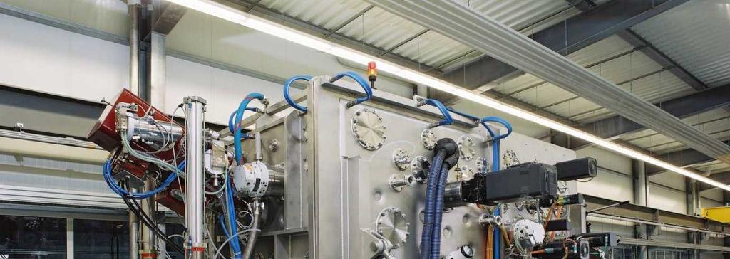
8 Introduction Advantages and limitations of SAD: + High plasma densities with 60% ionisation degree can be achieved. + The additional equipment in the process-surrounding of the EB evaporator is less expensive than other plasma generation tools. + The position of the arc on the evaporant coincides with the location of the electron beam generated vapor source. Therefore the activated vapor distribution may be similar to the initial EB vapor distribution. - Only some refractory metals allow the ignition of a diffuse arc on the evaporant. Examples: Mo, Zr, Ta, W, Ti. Questions regarding coating of titanium and its compounds: Which coating rates can be achieved today using SAD in case of titanium and its compounds titanium dioxide and titanium nitride? Which layer properties can be achieved by means of SAD? Is it possible to extend the SAD process to large area dimensions? 8

9 Description of Experiments Stage 1: Free span metal strip coating Technical data of the lab coater MAXI: Max. strip width: 280 mm Max. strip thickness: 500 µm Max. substrate speed: 60 m/min 1 Unwinder 2 Heating 3 Sputter etching 4 EB gun 5 Crucible (cathode) 6 Anode 7 Gas manifold 8 Measurement devices 9 Upwinder 9
10 Description of Experiments Stage 1: Free span steel strip coating Feature Titanium Titanium oxide Titanium nitride Crucible Cooled copper Cooled copper Cooled copper Evaporant Titanium Titanium Titanium EB acc. voltage 40 kv 40 kv 40 kv EB power 60 kw 27 kw 17 kw Process gas / Oxygen Nitrogen Gas flow / sccm 2000 sccm Proc. pressure 2 x 10e-5 mbar 2.3 x 10e-3 mbar 2 x10e-3 mbar Arc current 200 A A 100 A Bias voltage / 130 V pulsed DC 100 V pulsed DC Measurements: Layer thickness: GDEOS, Ellipsometry Optical constants: Ellipsometry Hardness: Nanoindentation 10
 8 Anode 9 Gas manifold")
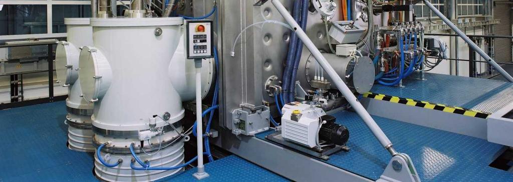
11 Description of Experiments Stage 2: Metal foil coating on a cooling drum Winding system 2 IR heater 3 Glow discharge 4 Sputtering 5 EB gun 6 Cooling drum 7 Crucible system (cathode) 8 Anode 9 Gas manifold 11

12 Description of Experiments Stage 2: Metal foil coating on a cooling drum Process enlargement: - Doubling of the substrate width - Doubling of the coating distance - Coating of thin stainless steel foils EB-figure: Double source: Jumping beam; Two filled ellipses Distance 600 mm Technical data of FOBA 600: Substrate width 600 mm Substrate thickness µm Max. speed 1000 m/min Movable cooled copper crucible Temperature cooling drum: -20 C 12
13 Description of Experiments Stage 2: Metal foil coating on a cooling drum Feature Crucible Evaporant EB acc. voltage EB power Process gas Gas flow Proc. pressure Arc current Bias voltage Measurements: Titanium Titanium oxide Titanium nitride Cooled copper Cooled copper Cooled copper Titanium Titanium Titanium 60 kv 60 kv 60 kv 100 kw 52 kw 44 kw / Oxygen Nitrogen / 8000 sccm 4000 sccm < 1 x 10e-4 mbar 2 x 10e-3 mbar 2 x 10e-3 mbar 1000 A 800 A 600 A / 120 V pulsed DC 120 V pulsed DC Layer thickness: GDEOS, ellipsometry Optical constants: Spectral ellipsometry 13
14 Coating Results Stage 1: Free span metal strip coating Feature Titanium Titanium oxide Titanium nitride Coating rate 400 nm/s nm/s 30 nm/s Dyn. dep. rate 5500 nm x m/min nm x m/min 420 nm x m/min Appearance metallic brilliant transparent golden Optical constants n(550nm) = k(550nm) 0.01 Hardness Process stability: 2h (limitation by crucible) Dense plasma on the evaporant 7 10 GPa Diffuse arc is steered by the hottest zone on the titanium melt (electron beam impingement) 30 GPa 14
15 Coating Results Stage 1: Free span metal strip coating Refractive index at various coating rates depends on: Reactive gas inlet Substrate temperature Arc parameters Bias voltage Titanium dioxide refractive index at various SAD rates 15

16 Results of Process Enlargement Stage 2: Metal foil coating on a cooling drum a) EB-evaporation without SAD b) Start of SAD: diffuse arc ignition c) High density plasma of the SAD process Double source distribution: Distance of two EB heated zones up to 600 mm Diffuse arc is split and steered by both overheated regions One anode for two sources Large area SAD by superposition of two plasma generation zones 16
17 Results of Process Enlargement Stage 2: Results of metal foil coating on a cooling drum Feature Coating rate Dyn. dep. rate Appearance Optical constants Hardness Titanium oxide 50 nm/s 600 nm x m/min transparent n(550nm) = 2.3 k(550nm) 0.01 Titanium nitride 36 nm/s 430 nm x m/min golden 33 GPa Double source reactive SAD allows long term stable and homogeneous deposition of extended substrates with coatings from titanium compounds. Crucible movement lead to an increased process duration of 8h. High rates can be achieved in spite of reduced vapor utilization (increased coating distance). 17
18 Results of Process Enlargement Stage 2: Metal foil coating on a cooling drum Layer thickness s(nm) Position across the substrate x(mm) Average layer thickness distribution of the titanium dioxide coating 18
19 Conclusions and Outlook Titanium and its compounds can be coated by means of (reactive) SAD at high and stable rates. The dynamic deposition rate of titanium dioxide amounts to approximately 1000 nm x m/min. Comparison 1: The same rate can be achieved with more than 20 dual cylindrical magnetrons. This means that the equipment costs of SAD compared with sputtering solutions are considerably lower. There is the possibility of substitution of expensive titanium suboxides as evaporant by low cost titanium. Comparison 2: The price of Ti 3 O 5 is about 140 USD/kg. Compared with this the price of titanium is only about 5 USD/kg. This means that the coating costs can be reduced drastically in the case of reactive SAD. The experiments have displayed that the SAD process can be extended to a large area technology. There are no limitations regarding substrate widths. The way into several industrial applications is opened now. 19
20 Conclusions and Outlook Coatings from titanium and its compounds on various substrates and their applications: Coating Titanium Titanium oxide Substrate Stainless steel Aluminum Aluminum Stainless steel, ceramics Application Catalysts Roof elements Enhanced reflectors Photocatalytic applications Titanium oxynitride Titanium nitride Copper Steel, others Solar absorbers Decorative coatings Fuel cells SAD can be expected in these industrial application fields! 20

21 Thank you for your kind attention! 21
22 BACK TO LIST
Thermal Load And Heat Transfer Regarding EBPVD Of Plastic Web And Thin Metal Foils
 Thermal Load And Heat Transfer Regarding EBPVD Of Plastic Web And Thin Metal Foils J. Richter, E. Reinhold, Chr. Steuer VON ARDENNE Anlagentechnik GmbH D-01324 Dresden, Germany 1 - Thema - 12.08.2003 e-mail:
Electron beam technology for turbine coating
 Второй международный технологический форум "Инновации. Технологии. Производство." 23-25 марта 2015 года Electron beam technology for turbine coating Anastasiya Zagorni, MBA Prof. Dr. Christoph Metzner,
Roll-to-roll Technology for Transparent High Barrier Films
 Roll-to-roll Technology for Transparent High Barrier Films Presented at the AIMCAL Fall Technical Conference, October 19-22, 2008, Myrtle Beach, SC, USA Nicolas Schiller, John Fahlteich, Matthias Fahland,
Mass Production of Clear Barriers. Requirements on Vacuum Web Coaters for Quality Assurance. Rainer Ludwig, Applied Films, Alzenau, Germany.
 Mass Production of Clear Barriers Requirements on Vacuum Web Coaters for Quality Assurance Rainer Ludwig, Applied Films, Alzenau, Germany Abstract An increasing number of packages using Transparent Barrier
Applied Research for Vacuum Web Coating: What is Coming Next?
 Applied Research for Vacuum Web Coating: What is Coming Next? Matthias Fahland, John Fahlteich, Steffen Günther, Manuela Junghähnel, Claus Luber, Nicolas Schiller, Cindy Steiner, Steffen Straach, Michiel
Vacuum Deposition of High Performance Gas Barrier Materials for Electronics Applications
 Vacuum Deposition of High Performance Gas Barrier Materials for Electronics Applications Hélène Suttle DPhil Research Student Department of Materials -University of Oxford AIMCAL Fall Conference October
Transactions on Engineering Sciences vol 2, 1993 WIT Press, ISSN
 A study of thin-film continuous coating process by vapour deposition P. Gimondo," F. Arezzo,* B. Grifoni,* G. Jasch& "Centra Sviluppo Materiali SpA, Via di Castel & Von Ardenne Anlagentchnik GmbH, Plattleite
Photovoltaics & Solar Thermals. Thin-film equipment. Customized. FHR Anlagenbau GmbH I
 Photovoltaics & Solar Thermals Thin-film equipment. Customized. FHR Anlagenbau GmbH I www.fhr.de FHR Anlagenbau GmbH is an innovative enterprise in the branch of vacuum processing and thin-film technologies.
High Rate low pressure PECVD for barrier and optical coatings
 High Rate low pressure PECVD for barrier and optical coatings, Matthias Fahland, John Fahlteich, Björn Meyer, Steffen Straach, Nicolas Schiller Outline Introduction PECVD New developments magpecvd arcpecv
High Rate Deposition of Reactive Oxide Coatings by New Plasma Enhanced Chemical Vapor Deposition Source Technology
 General Plasma, Inc. 546 East 25th Street Tucson, Arizona 85713 tel. 520-882-5100 fax. 520-882-5165 High Rate Deposition of Reactive Oxide Coatings by New Plasma Enhanced Chemical Vapor Deposition Source
AC Reactive Sputtering with Inverted Cylindrical Magnetrons
 AC Reactive Sputtering with Inverted Cylindrical Magnetrons D.A. Glocker, Isoflux Incorporated, Rush, NY; and V.W. Lindberg and A.R. Woodard, Rochester Institute of Technology, Rochester, NY Key Words:
Vacuum Equipment for TCO and AR Coatings Deposition by Reactive Magnetron Sputtering
 Vacuum Equipment for TCO and AR Coatings Deposition by Reactive Magnetron Sputtering E. Yadin; V. Kozlov; E. Machevskis, Sidrabe, Inc., 17 Krustpils str.,riga, LV1073, Latvia. Tel: +371 7249806, Fax: +371
High Productive Deposited Mo Layers for Back Ohmic Contacts of Solar Cells
 Full Paper High Productive Deposited Mo Layers for Back Ohmic Contacts of Solar Cells Jens-Peter Heinß,* Frank Händel, Toni Meyer, Roland Würz In the paper, thin molybdenum (Mo) layers produced by magnetron
From Vacuum to Atmosphere and back an in-house Process Chain for Different Products
 From Vacuum to Atmosphere and back an in-house Process Chain for Different Products Dr. Steffen Günther Vacuum coating low pressure 10-1 10-4 Pa (10-3 10-6 mbar) unhindered particle movement no unintended
New Dual Magnetron Plasma Source Designed For Large Area Substrate Pretreatment and Oxide Film Deposition P. Morse, R. Lovro, M. Rost, and J.
 New Dual Magnetron Plasma Source Designed For Large Area Substrate Pretreatment and Oxide Film Deposition P. Morse, R. Lovro, M. Rost, and J. German, Road Map Source Design Theory of Operation Experimental
Solar Selective Absorber Coating Methods Plasma Processes
 Solar Selective Absorber Coating Methods Plasma Processes Paul Gantenbein & Elimar Frank SPF - Institut für Solartechnik University of Applied Sciences Rapperswil (HSR) Optical properties of a selective
ITO SPUTTER COATED FILMS FOR TOUCH PANEL APPLICATIONS USING ROTARY SINTERED CERAMIC ITO TARGETS: WHAT CAN BE LEARNED FROM GLASS COATING?
 ITO SPUTTER COATED FILMS FOR TOUCH PANEL APPLICATIONS USING ROTARY SINTERED CERAMIC ITO TARGETS: WHAT CAN BE LEARNED FROM GLASS COATING? Paul Lippens AIMCAL Web coating conference 2012 Outline Introduction
THE INFLUENCE OF NITROGEN CONTENT ON THE MECHANICAL PROPERTIES OF TiN x THIN FILMS PREPARED BY REACTIVE MAGNETRON SPUTTERING
 Bulletin of the Transilvania University of Braşov Series I: Engineering Sciences Vol. 5 (54) No. 2-2012 THE INFLUENCE OF NITROGEN CONTENT ON THE MECHANICAL PROPERTIES OF TiN x THIN FILMS PREPARED BY REACTIVE
Titanium Oxide S Patinal
 Product Information Titanium Oxide S GENERAL INFORMATION Titanium Oxide S is one of the preferred Ti-suboxides used to manufacture thin films of TiO2. For this purpose the material is evaporated reactively.
Titanium Oxide(II) Patinal Titanium Oxide(III) Patinal Titanium Oxide(IV) Patinal
 Patinal Titanium Oxide(III) Patinal Titanium Oxide(IV) Patinal") Product Information Titanium Oxide(II) Patinal Titanium Oxide(III) Patinal Titanium Oxide(IV) Patinal GENERAL INFORMATION A number of titanium (sub)oxides, e.g. TiO, Ti2O3, TiO2, can be used as evaporation
Product Information Titanium Oxide(II) Patinal Titanium Oxide(III) Patinal Titanium Oxide(IV) Patinal GENERAL INFORMATION A number of titanium (sub)oxides, e.g. TiO, Ti2O3, TiO2, can be used as evaporation
Titanium Oxide X Patinal
 Product Information Titanium Oxide X Patinal GENERAL INFORMATION Titanium Oxide X Patinal (chemical formula Ti3O5) is one of the preferred Ti-suboxides used to manufacture thin films of TiO2. For this
1 Introduction. 2 Basic Technology
 Innovative Clear Barrier Technology for the Packaging Industry Nicolas Schiller 1, Steffen Straach, Steffen Günther Fraunhofer FEP, Germany Alexandra L. Quiceno G., Antonio García Contreras BIOFILM, Columbia
Hafnium(IV) Oxide Patinal
 Oxide Patinal") Product Information Hafnium(IV) Oxide Patinal GENERAL INFORMATION Hafnium oxide is used for thin films with high refractive index in AR coatings, filters, mirrors, and beam splitters for the spectral region
Product Information Hafnium(IV) Oxide Patinal GENERAL INFORMATION Hafnium oxide is used for thin films with high refractive index in AR coatings, filters, mirrors, and beam splitters for the spectral region
Advanced Glass Refinement by Thin Films - Trends and Challenges of Thin Film Technologies for Windows and Facade Glasses
 Advanced Glass Refinement by Thin Films - Trends and Challenges of Thin Film Technologies for Windows and Facade Glasses Dr.-Ing. Manuela Junghähnel Fraunhofer Institute for Elect ron Beam and Plasma Technology
Advanced Sheet-to-Sheet and Roll-to-Roll thin-film processing on ultra-thin flexible glass for flexible electronic devices
 Advanced Sheet-to-Sheet and Roll-to-Roll thin-film processing on ultra-thin flexible glass for flexible electronic devices M. Junghaehnel 1, J. Westphalen 1, F. Naumann 2, G. Lorenz 2, M. Fahland 1, S.
Latest Development in Vacuum Metallisation
 Latest Development in Vacuum Metallisation Professor Nadir Ahmed Vacuum Metallising Consultant General Vacuum Equipment Ltd. Pennine Business Park, Pilsworth Road, Heywood OL10 2TL England Tel: +44(0)1706
ARTICLE IN PRESS. Materials Science in Semiconductor Processing
 Materials Science in Semiconductor Processing ] (]]]]) ]]] ]]] Contents lists available at ScienceDirect Materials Science in Semiconductor Processing journal homepage: www.elsevier.com/locate/mssp High-dielectric
METHODS OF COATING FABRICATION
 METHODS OF COATING FABRICATION Zbigniew Grzesik http://home.agh.edu.pl/~grzesik Department of Physical Chemistry and Modelling DEFINITION The coating is the thin outer layer of the object, which physiochemical
Physical Vapor Deposition (PVD) Zheng Yang
 Zheng Yang") Physical Vapor Deposition (PVD) Zheng Yang ERF 3017, email: yangzhen@uic.edu Page 1 Major Fabrication Steps in MOS Process Flow UV light Mask oxygen Silicon dioxide photoresist exposed photoresist oxide
Physical Vapor Deposition (PVD) Zheng Yang ERF 3017, email: yangzhen@uic.edu Page 1 Major Fabrication Steps in MOS Process Flow UV light Mask oxygen Silicon dioxide photoresist exposed photoresist oxide
Thin Films: Sputtering Systems (Jaeger Ch 6 & Ruska Ch 7,) Can deposit any material on any substrate (in principal) Start with pumping down to high
 Can deposit any material on any substrate (in principal) Start with pumping down to high") Thin Films: Sputtering Systems (Jaeger Ch 6 & Ruska Ch 7,) Can deposit any material on any substrate (in principal) Start with pumping down to high vacuum ~10-7 torr Removes residual gases eg oxygen from
Thin Films: Sputtering Systems (Jaeger Ch 6 & Ruska Ch 7,) Can deposit any material on any substrate (in principal) Start with pumping down to high vacuum ~10-7 torr Removes residual gases eg oxygen from
Linear Plasma Sources for Surface Modification and Deposition for Large Area Coating
 Linear Plasma Sources for Surface Modification and Deposition for Large Area Coating Dr Tony Williams Gencoa Ltd, UK Victor Bellido-Gonzalez, Dr Dermot Monaghan, Dr Joseph Brindley, Robert Brown SVC 2016,
Vacuum plasma treatment and coating of fluoropolymer webs challenges and applications
 Vacuum plasma treatment and coating of fluoropolymer webs challenges and applications AIMCAL 2016 Cindy Steiner John Fahlteich Dresden, 01.06.2016 page 1 Ethylene Tetrafluoroethylene (ETFE) semi-crystalline
Thermal Evaporation. Theory
 Thermal Evaporation Theory 1. Introduction Procedures for depositing films are a very important set of processes since all of the layers above the surface of the wafer must be deposited. We can classify
Substance L5 and L5 HD Patinal
 Product Information Substance L5 and L5 HD GENERAL INFORMATION Substance L5 is a low refractive index mixture of silicon dioxide and aluminium oxide. It was developed to provide an evaporation material
Ellipsometry as a tool for identifying process issues in roll-to-roll sputter deposited metal-oxide coatings
 Ellipsometry as a tool for identifying process issues in roll-to-roll sputter deposited metal-oxide coatings Sharon Louch Centre for Process Innovation, Wilton Centre, edcar. UK. TS10 3H Abstract Ellipsometry
Linear Broad Beam Ion Sources ACC-30x150 IS, ACC-40x300 IS and ACC-40 x 600 IS
 Dr. Hermann Schlemm Ion Beam- and Surface Technology Saalbahnhofstraße 6 D - 07743 JENA, Germany Tel.: ++ 49 3641 22 73 29 Fax: ++ 49 3641 22 87 60 email: hermann.schlemm@jenion.de http://www.jenion.de
Ageing Resistance (12 years) of Hard and Oxidation Resistant SiBCN Coatings
 of Hard and Oxidation Resistant SiBCN Coatings") Ageing Resistance (12 years) of Hard and Oxidation Resistant SiBCN Coatings Jiri Houska Department of Physics and NTIS - European Centre of Excellence, University of West Bohemia, Czech Republic Acknowledgment
Ageing Resistance (12 years) of Hard and Oxidation Resistant SiBCN Coatings Jiri Houska Department of Physics and NTIS - European Centre of Excellence, University of West Bohemia, Czech Republic Acknowledgment
Productivity versus Profitability in Vacuum Web Coating
 Productivity versus Profitability in Vacuum Web Coating Liz Josephson, Applied Films Corp., Longmont, USA Dirk Hoffmann, Applied Films GmbH & Co KG, Alzenau, Germany Gerard Loebig, Applied Films GmbH &
Optical Coatings. Photonics 4 Luxury Coatings , Genève. Dr. Andreas Bächli Head of Optical Coatings at RhySearch, Buchs (SG)
") Optical Coatings Photonics 4 Luxury Coatings 21.06.2017, Genève Dr. Andreas Bächli Head of Optical Coatings at RhySearch, Buchs (SG) RhySearch The Research- and Innovation Center in the Rhine Valley RhySearch
Optical Coatings Photonics 4 Luxury Coatings 21.06.2017, Genève Dr. Andreas Bächli Head of Optical Coatings at RhySearch, Buchs (SG) RhySearch The Research- and Innovation Center in the Rhine Valley RhySearch
Thin Films: Sputtering Systems (Jaeger Ch 6 & Ruska Ch 7,) Sputtering: gas plasma transfers atoms from target to substrate Can deposit any material
 Sputtering: gas plasma transfers atoms from target to substrate Can deposit any material") Thin Films: Sputtering Systems (Jaeger Ch 6 & Ruska Ch 7,) Sputtering: gas plasma transfers atoms from target to substrate Can deposit any material on any substrate (in principal) Start with pumping down
Thin Films: Sputtering Systems (Jaeger Ch 6 & Ruska Ch 7,) Sputtering: gas plasma transfers atoms from target to substrate Can deposit any material on any substrate (in principal) Start with pumping down
Maximizing the Potential of Rotatable Magnetron Sputter Sources for Web Coating Applications
 Maximizing the Potential of Rotatable Magnetron Sputter Sources for Web Coating Applications V.Bellido-Gonzalez, Dermot Monaghan, Robert Brown, Alex Azzopardi, Gencoa, Liverpool UK Structure of presentation
Oerlikon PVD production solutions for piezoelectric materials
 Oerlikon PVD production solutions for piezoelectric materials Workshop PiezoMEMS Aachen,18. /19.05.2010 M. Kratzer Oerlikon Systems R&D Oerlikon company and products Thin films used for SAW, BAW, MEMS,
EE 5344 Introduction to MEMS. CHAPTER 3 Conventional Si Processing
 3. Conventional licon Processing Micromachining, Microfabrication. EE 5344 Introduction to MEMS CHAPTER 3 Conventional Processing Why silicon? Abundant, cheap, easy to process. licon planar Integrated
Previous Lecture. Vacuum & Plasma systems for. Dry etching
 Previous Lecture Vacuum & Plasma systems for Dry etching Lecture 9: Evaporation & sputtering Objectives From this evaporation lecture you will learn: Evaporator system layout & parts Vapor pressure Crucible
Gas and surface applications of atmospheric pressure plasmas
 Gas and surface applications of atmospheric pressure plasmas Eugen Stamate Technical University of Denmark Roskilde 4000, Denmark OUTLINE Introduction of DTU Energy Conversion and Storage Activities in
4-in-1 Nano Machine & Technology
 4-in-1 Nano Machine & Technology Machine combines 1) CVD, 2) PVD, 3) ion saturation and 4) ion-treatment processes in one (1) production cycle in one machine that produces functional coatings used to harden
PLASMA FLOW AND PLASMA EXPANSION AROUND 3D OBJECTS IN METAL PLASMA IMMERSION ION IMPLANTATION
 PLASMA FLOW AND PLASMA EXPANSION AROUND 3D OBJECTS IN METAL PLASMA IMMERSION ION IMPLANTATION Darina Manova & Stephan Mändl 1 Motivation 2 Motivation Visualisation of Water Flow from Dynamic Sand Dunes
EVALUATION OF ADHESION, HARDNESS AND MICROSTRUCTURE OF CrN e CrAlN COATINGS DEPOSITED BY HIGH POWER IMPULSE MAGNETRON SPUTTERING
 EVALUATION OF ADHESION, HARDNESS AND MICROSTRUCTURE OF e CrAlN COATINGS DEPOSITED BY HIGH POWER IMPULSE MAGNETRON SPUTTERING Bruno César Noronha Marques de Castilho, Mechanical Engineering - Materials,
Comparison of Different Sputter Processes for ITO: Planar DC versus Planar AC
 Comparison of Different Sputter Processes for ITO: Planar DC versus Planar AC P. Sauer, H.-G. Lotz, A. Hellmich, R. Kukla, J. Schröder Applied Films GmbH & Co. KG, Alzenau, Germany Key Words: ITO MF PET
Energy-efficient glazing
 Energy-efficient glazing Low-E solar reflective coatings Float glass is traditionally used in the building and automotive industries to provide both clear and tinted transparent barriers to the elements.
INTRODUCTION OF SYS & System
 Vision 2015 INTRODUCTION OF SYS & System PVD & Ion Beam Irradiator Manufacturing Company isys is committed to building the best January. 2007 1 SYS, based on excellent technology and sufficient equipment
Plasma Quest Limited
 Plasma Quest Limited A Remote Plasma Sputter Process for High Rate Web Coating of Low Temperature Plastic Film with High Quality Thin Film Metals and Insulators Dr. Peter Hockley and Prof. Mike Thwaites,
micro resist technology
 Characteristics Processing guidelines Negative Tone Photoresist Series ma-n 1400 ma-n 1400 is a negative tone photoresist series designed for the use in microelectronics and microsystems. The resists are
THIN NICKEL OXIDE LAYERS PREPARED BY ION BEAM SPUTTERING: FABRICATION AND THE STUDY OF ELECTROPHYSICAL PARAMETERS
 THIN NICKEL OXIDE LAYERS PREPARED BY ION BEAM SPUTTERING: FABRICATION AND THE STUDY OF ELECTROPHYSICAL PARAMETERS Pavel HORÁK a,b, Václav BEJŠOVEC b, Vasyl LAVRENTIEV b, Jiří VACÍK b, Martin VRŇATA a,
 This article was originally published in a journal published by Elsevier, and the attached copy is provided by Elsevier for the author s benefit and for the benefit of the author s institution, for non-commercial
Substance M2 Patinal GENERAL INFORMATION AREAS OF APPLICATION THIN FILM PROPERTIES. Product Information
 Product Information Substance M2 Patinal GENERAL INFORMATION Substance M2 Patinal (Aluminium Lanthanum Oxide) is a medium refractive index material for evaporation, covering a wide spectral range from
needed for the SOFC electrolyte membrane application. Few directed vapor deposition
 Chapter 3 Experimental Procedure 3.1 Overview Prior to this study, DVD has not been used to create the type of dense metal oxide layers needed for the SOFC electrolyte membrane application. Few directed
2.3.3 Plasma Sulphurizing Restriction of Plasma Nitriding Development of Plasma Nitriding in China References...
 Contents 1 Introduction... 1 1.1 Engineering Materials and Its Surface.... 1 1.2 Surface Engineering and Its Classification... 2 1.2.1 Concept of Surface Engineering... 2 1.2.2 Surface Hardening Technology...
MODULAR PROCESS SYSTEMS ADVANCED COATING EQUIPMENT ADVANCED COATING EQUIPMENT
 MODULAR PROCESS SYSTEMS ADVANCED COATING EQUIPMENT MODULAR PROCESS SYSTEMS ADVANCED COATING EQUIPMENT APPLICATIONS VON ARDENNE is your partner of choice if you are looking for systems with a modular design
Metallization deposition and etching. Material mainly taken from Campbell, UCCS
 Metallization deposition and etching Material mainly taken from Campbell, UCCS Application Metallization is back-end processing Metals used are aluminum and copper Mainly involves deposition and etching,
On the way to the latest packaging R2R Metallizer
 On the way to the latest packaging R2R Metallizer AIMCAL FALL Conference 2011 Schmid Vacuum Technology GmbH, Karlstein, Germany Peter Sauer Gerard Löbig Andre Herzog Johannes Krantz Michael Klosch-Trageser
A Basic Introduction to Thin-Film Coatings. From the Experts at VaporTech
 A Basic Introduction to Thin-Film Coatings From the Experts at VaporTech What are thin-film coatings? 2018 Vapor Technologies, Inc. All rights reserved. Thin-film coatings Physical or Chemical Vapor Deposition
APPLICATION-DRIVEN PRODUCTIVE VACUUM TECHNOLOGY
 FRAUNHOFER INSTITUTE FOR ELECTRON BEAM AND PLASMA TECHNOLOGY FEP SPECIAL SEMINAR APPLICATION-DRIVEN PRODUCTIVE VACUUM TECHNOLOGY APRIL 15, 2014 SOKOLNIKI ECC PROGRAM TUESDAY, APRIL 15 TH 10:15 10:20 Opening
HiPIMS Technology: advantages and disadvantages
 Vacuum plasma technology HiPIMS Technology: advantages and disadvantages Cr - DC Cr - HiPIMS Alessandro Patelli alessandro.patelli@venetonanotech.it Outline 1. What is HiPIMS Ti target surface 2. What
Properties of Highly Transparent Conductive Ga-Doped ZnO Films prepared on Polymer Substrates by Reactive Plasma Deposition with DC Arc Discharge
 Journal of Photopolymer Science and Technology Volume 22, Number 4 (2009) 497-502 2009 CPST Properties of Highly Transparent Conductive Ga-Doped ZnO Films prepared on Polymer Substrates by Reactive Plasma
Effective Closed-Loop Control for Reactive Sputtering Using Two Reactive Gases
 Effective Closed-Loop Control for Reactive Sputtering Using Two Reactive Gases D.C. Carter, W.D. Sproul, and D.J. Christie, Advanced Energy Industries, Inc., Fort Collins, CO Key Words: Reactive sputtering
Gencoa Product Portfolio
 Gencoa offer the following range of products & process technology for the thin film industry developed over the last 20 years Planar Magnetrons Plasma Pre- Treaters Reactive Gas Controllers Gencoa Product
Large Area Coating for Glazing IOP Vacuum Symposium Daresbury 11 th Feb 2010
 Large Area Coating for Glazing IOP Vacuum Symposium Daresbury 11 th Feb 2010 Off-Line Coatings Technology Group Pilkington European Technology Centre 2 NSG Group Pilkington a member of NSG Group from June
NASF SURFACE TECHNOLOGY WHITE PAPERS 83 (1), 7-12 (October 2018) Advances in Decorative PVD Chromium Coatings for Polymer Substrates
, 7-12 (October 2018) Advances in Decorative PVD Chromium Coatings for Polymer Substrates") Advances in Decorative PVD Chromium Coatings for Polymer Substrates A Synopsis * of a Presentation given at SUR/FIN 2018 (Cleveland, Ohio) by Gary Vergason ** Vergason Technology, Inc. Van Etten, New York,
Advances in Decorative PVD Chromium Coatings for Polymer Substrates A Synopsis * of a Presentation given at SUR/FIN 2018 (Cleveland, Ohio) by Gary Vergason ** Vergason Technology, Inc. Van Etten, New York,
A Plasma Emission Controller for Reactive. Magnetron Sputtering of Titanium Dioxide Films
 Adv. Theor. Appl. Mech., Vol. 5, 2012, no. 1, 1-10 A Plasma Emission Controller for Reactive Magnetron Sputtering of Titanium Dioxide Films Raad A. Swady DMPS, College of Arts & Sciences, University of
PRECISION OPTICAL FILTERS BY EOSS - ENHANCED OPTICAL SPUTTERING SYSTEM. Fraunhofer
 PRECISION OPTICAL FILTERS BY EOSS - ENHANCED OPTICAL SPUTTERING SYSTEM EOSS ENHANCED OPTICAL SPUTTERING SYSTEM Fraunhofer IST, Braunschweig Contact: Dr. M. Vergöhl +49 531 2155 640 EOSS Coating System
Comparison of Carbon Coatings Deposited by Different Techniques
 Comparison of Carbon Coatings Deposited by Different Techniques V. Gorokhovsky, K.Coulter, M.Miller, R.Wei, C. Ellis, C.Engel Southwest Research Institute San Antonio, Texas Funded by SwRI: Project No.
PROPERTIES OF MATERIALS PART HARDNESS
 CHAPTER 3 PROPERTIES OF MATERIALS PART 2 30.07.2007 3.1.10 HARDNESS A Resistance to permanently indenting the surface Large hardness means resistance to plastic deformation or cracking In compression,
Vacuum deposition of TiN
 J.Lorkiewicz DESY.27.10.02 Vacuum deposition of TiN (TiN coating of high power coupler elements as an anti-multipactor remedy at DESY) The scope of the project: - reducing secondary electron emission and
Improvement of gas barrier properties by combination of polymer film and gas barrier layer
 Improvement of gas barrier properties by combination of polymer film and gas barrier Y. Tsumagari, H. Murakami, K. Iseki and S. Yokoyama Toyobo Co., LTD. RESEARCH CENTER, - Katata 2-chome, Otsu, Shiga,
Energy Efficient Glazing Design. John Ridealgh Off-Line Coatings Technology Group Pilkington European Technology Centre
 Energy Efficient Glazing Design John Ridealgh Off-Line Coatings Technology Group Pilkington European Technology Centre 2 John Ridealgh 30th November 2009 Talk Outline Pilkington Group Limited & NSG Group
Ion-plasma technologies and equipment
 Ion-plasma technologies and equipment VACUUM ION-PLASMA INSTALLATIONS OF «OPAL» SERIES «Opal» series ion-plasma installations are designed for deposition of low-emission, reflective and toned coatings
Lecture Day 2 Deposition
 Deposition Lecture Day 2 Deposition PVD - Physical Vapor Deposition E-beam Evaporation Thermal Evaporation (wire feed vs boat) Sputtering CVD - Chemical Vapor Deposition PECVD LPCVD MVD ALD MBE Plating
COMPARISON OF FRICTIONAL CHARACTERISTICS OF TITANIUM NITRIDE FILMS PRODUCED BY ECR-DC SPUTTERING AND PVD
 THE ANNALS OF UNIVERSITY DUNĂREA DE JOS OF GALAŢI 23 ISSN 1221-459 123 COMPARISON OF FRICTIONAL CHARACTERISTICS OF TITANIUM NITRIDE FILMS PRODUCED BY ECR-DC SPUTTERING AND PVD Constantin Rânea 1, Cristian
Overview of Advanced Surface Science activities at CERN. S.Calatroni, M.Taborelli TE-VSC-SCC
 Overview of Advanced Surface Science activities at CERN S.Calatroni, M.Taborelli TE-VSC-SCC Basic components of particle accelerators Technology Department 10 October 2014 S. Calatroni & M. Taborelli 2
Crystallization of Amorphous Silicon Thin Film. by Using a Thermal Plasma Jet. Hyun Seok Lee, Sooseok Choi, Sung Woo Kim, and Sang Hee Hong*
 Crystallization of Amorphous Silicon Thin Film by Using a Thermal Plasma Jet Hyun Seok Lee, Sooseok Choi, Sung Woo Kim, and Sang Hee Hong* Department of Nuclear Engineering, Seoul National University Seoul
Platypus Gold Coated Substrates. Bringing Science to the Surface
 Platypus Gold Coated Substrates Bringing Science to the Surface Overview Gold Coated Substrates - Gold Coating Introduction - Glossary of Terms - Gold Coating Methods - Critical Features Platypus Gold
Dr. Sabrina Lee and Dr. Rong Wei NDIA Gun and Missile Conference, New Orleans, LA April 21-24, 2008
 Weapon Systems & Technology Directorate US ARMY ARDEC- BENÉT LABS TITLE: PLASMA ENHANCED MAGNETRON TECHNOLOGY FOR DURABLE POLLUTION-FREE COATINGS Dr. Sabrina Lee and Dr. Rong Wei NDIA Gun and Missile Conference,
High Quality Multi-arc Targets
 High Quality Multi-arc Targets IKS provides high-quality multi-arc targets for a wide range of applications for ferromagnetic, complex oxides, and semiconducting films. Our targets are offered in various
Semiconductor Manufacturing Technology. IC Fabrication Process Overview
 Semiconductor Manufacturing Technology Michael Quirk & Julian Serda October 00 by Prentice Hall Chapter 9 IC Fabrication Process Overview /4 Objectives After studying the material in this chapter, you
Growth Of TiO 2 Films By RF Magnetron Sputtering Studies On The Structural And Optical Properties
 Journal of Multidisciplinary Engineering Science and Technology (JMEST) Growth Of TiO 2 Films By RF Magnetron Sputtering Studies On The Structural And Optical Properties Ahmed K. Abbas 1, Mohammed K. Khalaf
TANOS Charge-Trapping Flash Memory Structures
 TANOS Charge-Trapping Flash Memory Structures A Senior Design by Spencer Pringle 5/8/15 Table of Contents Motivation Why Charge-Trapping Flash (CTF)? Charge-Trapping vs. Floating Gate Electronically-Erasable
Comparison of Different Sputter Processes for ITO: Planar DC versus Planar AC
 Comparison of Different Sputter Processes for ITO: Planar DC versus Planar AC P. Sauer,H.-G.Lotz, A. Hellmich R. Kukla, J. Schröder Applied Films GmbH &,Co. KG, Alzenau, Germany Outline n n n n n n Current
Thin Film Gas Sensor. Nanoelectronics and MEMS Laboratory National Electronics and Computer Technology
 Ion-assisted E-beam E Evaporated Thin Film Gas Sensor A. Wisitsoraat,, A. A Tuantranont,, V. V Patthanasettakul, T. Lomas,, and P. Chindaudom Nanoelectronics and MEMS Laboratory National Electronics and
Effect of Glass Formation- Thin Films
 Effect of Glass Formation- Thin Films Kathleen Richardson Clemson University richar3@clemson.edu richar3@clemson.edu Structure of Glass: Effects of Formation - Films 1 Glass ancient transmission medium
The most efficient way of transforming sunlight into heat
 The most efficient way of transforming sunlight into heat TiNOX, The Energy Trap Decisive for highest performance of a solar absorber plate is: - highest possible absorption of solar radiation - minimum
CHEMICAL DEPTH PROFILING OF TOOL MATERIALS USING GLOW DISCHARGE OPTICAL EMISSION SPECTROSCOPY (GD-OES)
") CHEMICAL DEPTH PROFILING OF TOOL MATERIALS USING GLOW DISCHARGE OPTICAL EMISSION SPECTROSCOPY (GD-OES) T. Björk Swedish Institute for Metals Researc Drottning Kristinas väg 48 114 28 Stockholm Sweden Abstract
CHEMICAL DEPTH PROFILING OF TOOL MATERIALS USING GLOW DISCHARGE OPTICAL EMISSION SPECTROSCOPY (GD-OES) T. Björk Swedish Institute for Metals Researc Drottning Kristinas väg 48 114 28 Stockholm Sweden Abstract
Transparent Ultra-Barrier Film Production and Product Integration
 Transparent Ultra-Barrier Film Production and Product Integration Mark George, Martin Rosenblum, Jason Bloking Rex Chang Vitriflex Inc., 2350 Zanker Road, Suite 20, San Jose, CA 95131 Introduction Vitriflex
Influence of Spraying Conditions on Properties of Zr-Based Metallic Glass Coating by Gas Tunnel Type Plasma Spraying
 Influence of Spraying Conditions on Properties of Zr-Based Metallic Glass by Gas Tunnel Type Plasma Spraying KOBAYASHI Akira *, KURODA Toshio *, KIMURA Hisamichi ** and INOUE Akihisa ** Abstract Metallic
MINISTRY OF EDUCATION AND SCIENCE OF UKRAINE
 MINISTRY OF EDUCATION AND SCIENCE OF UKRAINE National Technical University of Ukraine "Igor Sikorsky Kyiv Polytechnic Institute" Faculty of Physical Engineering Departments physics of metals 1 Student
Oxidation behavior of Cu nanoclusters in hybrid thin films
 Oxidation behavior of Cu nanoclusters in hybrid thin films Harm Wulff,* Steffen Drache*, Vitezslav Stranak**, Angela Kruth*** *EMAU Greifswald, **South Bohemian University, Budweis, *** INP Greifswald
II. NEG THIN FILM DEPOSITION
 Deposition of Non-Evaporable Getter Thin Films and Vacuum Pumping Performances Ankit Sur Engineering Department, Wayne State University, Detroit, MI 48202 The ERL (Energy Recovery Linac) proposed at Cornell
High Performance Lithium Battery Anodes Using Silicon Nanowires
 Supporting Online Materials For High Performance Lithium Battery Anodes Using Silicon Nanowires Candace K. Chan, Hailin Peng, Gao Liu, Kevin McIlwrath, Xiao Feng Zhang, Robert A. Huggins and Yi Cui * *To
PRACTICAL DESIGN AND PRODOCTION OF OPTICAL THIN FILMS
 PRACTICAL DESIGN AND PRODOCTION OF OPTICAL THIN FILMS RONALD R.WILLEY LexaLite International Corporation Charlevoix, Michigan Marcel Dekker, Inc. New York Basel Hong Kong Contents From the Series Editor