12th International Workshop on RF Superconductivity. A.Frigo, G.Lanza, H.Padamsee, V.Palmieri, D.Tonini
|
|
|
- Allan Briggs
- 6 years ago
- Views:
Transcription

1 12th International Workshop on RF Superconductivity A.Frigo, G.Lanza, H.Padamsee, V.Palmieri, D.Tonini


2 CERN geometry C. Benvenuti, S. Calatroni, I.E. Campisi, P. Darriulat, M.A. Peck, R. Russo, A.-M. Valente, Study of the surface resistance of superconducting niobium films at 1.5 GHz, Physica C 316 (1999)


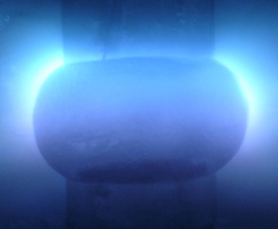
3 Cylindrical Magnetron Magnet Cavity Niobium cathode
4 Q-slope problem Bulk Niobium Niobium sputtered film

5 The INFN-LNL hypothesis Sputtering at different target-substrate angle Diploma thesis Morphology of Niobium Films Sputtered at Different Target-substrate Angles Diego Tonini, LNL-INFN, Material Science, Padova University.
 AFM Roughness images XRD spectras Diploma thesis Morphology of Niobium Films Sputtered at Different Target-substrate Angles Diego Tonini, LNL-INFN, Material Science, Padova")
6 At different target-substrate angle relative intensity degrees 60 degrees 45 degrees 30 degrees 15 degrees Theta (degrees) AFM Roughness images XRD spectras Diploma thesis Morphology of Niobium Films Sputtered at Different Target-substrate Angles Diego Tonini, LNL-INFN, Material Science, Padova University.
7 At different target-substrate angle Increasing level of contamination Superconducting properties Diploma thesis Morphology of Niobium Films Sputtered at Different Target-substrate Angles Diego Tonini, LNL-INFN, Material Science, Padova University.
8 At different target-substrate angle Increasing level of contamination Electrical properties Diploma thesis Morphology of Niobium Films Sputtered at Different Target-substrate Angles Diego Tonini, LNL-INFN, Material Science, Padova University.


9 Comparing Sputtering and Cathodic Arc Sputtered films grow along the normal to 110 crystal planes according to the atom arrival direction By cathodic arc, the substrate is biased; so ions always reach the substrate perpendicularly: NO TEXTURE vs target-substrate angle G. Keppel, V. Palmieri, N. Patron, D. Tonini, LNL-INFN
10 Understanding: Film morphology strictly correlated to the deposition angle Electrical and superconducting film properties degrade vs deposition angle Comprehension of sputtering principles is compulsory for conceiving new magnetron configurations
11 Deposition technique: magnetron sputtering B V e - V e // Uniform magnetic field lines ω c B

12 Deposition technique: magnetron sputtering E - Target ω m Non-uniform Magnetic field lines - Electron reflection is due to magnetostatic and electrostatic mirror
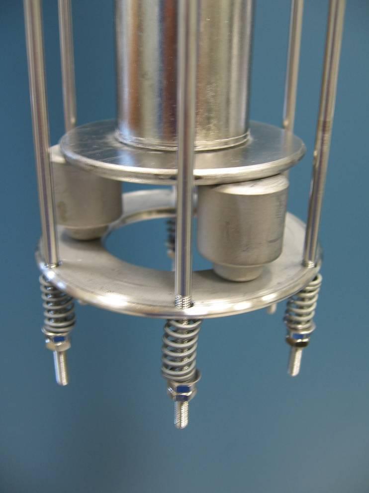
13 Deposition technique: magnetron sputtering Cylindrical Post Magnetron cathode E B B ω D 2 - B
14 Deposition technique: magnetron sputtering If E B - Cylindrical Post Magnetron cathode Higher ionisation efficiency B
15 Ideas to improve the film quality: 1. Increasing the sputtering rate R f i = N i N α i α i i + R ƒ i = Fraction of impurities trapped into the film α i = Impurities sticking coefficient N i = Number of atoms impurities arriving on the film surface

16 Target shape Plasma Target B 2 inches planar target

17 Target shape Plasma Target B 2 inches squared target
18 Target shape Plasma Target B 2 inches rounded target
 2,0 1,5 1,0 Planar target b = 6,9 0,5 200 220 240 260 280 300 320 Cathode potential")
19 Cathode shape modification 3,5 p = 2,5 * 10-2 mbar Fit: I = a*v b 3,0 2,5 Rounded target b = 9,0 Squared target b = 8,3 Increasing sputtering rate Current (A) 2,0 1,5 1,0 Planar target b = 6,9 0, Cathode potential (v)
20 Ideas to improve the film quality: 1. Increasing the sputtering rate R 2. Reducing the deposition angle

21 Cathode shape modification Cathode B E B // cathode surface Cavity B Magnet Higher deposition rate

22 Cathode shape modification Niobium ring positioned in the cell center

23 Cathode shape modification
24 Ideas to improve the film quality: 1. Increasing the sputtering rate R 2. Reducing the deposition angle 3. Promoting atoms rearrangement and impurities re-sputtering during film growing ( N ) iαi β fi = N α β + ( ) R i i ƒ i = fraction of impurities trapped into the film α i = impurities sticking coefficient N i = atoms impurities arriving on the film β = function of the bias current due to impurities ions R = sputtering rate


25 Biased Diode Sputtering Bias LNL Up to now The bias technique is highly reliable: over 40 QWRs are installed and working at LNL
26 Biased Magnetron Sputtering Magnet Cathode V Biased Grid +200 V Grounded Cavity


27 Biased Magnetron Sputtering Biased grid


28 Biased Magnetron Sputtering
29 Biased Magnetron Sputtering


30 Biased Magnetron Sputtering


31 Biased Magnetron Sputtering
32 Biased Magnetron Sputtering
33 Biased Magnetron Sputtering

34 Biased Magnetron Sputtering
35 Ideas to improve the film quality: 1. Increasing the sputtering rate R 2. Reducing the deposition angle 3. Promoting atoms rearrangement and impurities re-sputtering during film growing 4. Increase the cathode/substrate area ratio
36 Biased Diode Sputtering Bias CERN Low ratio cathode/substrate area Low sputtering rate (1 micron /day)


37 Cavity shaped cathode High ratio cathode/substrate area


38 Cavity shaped cathode in progress
39 Conclusion Three new magnetron sputtering configurations are ready!...soon 20 cavities to measure.
40
41 Cylindrical Post-Magnetron Magnetic field lines follow the cavity shape Cavity B Niobium cathode
DC magnetism of Niobium thin films
 Loughborough University Institutional Repository DC magnetism of Niobium thin films This item was submitted to Loughborough University's Institutional Repository by the/an author. Citation: WILDE, S....et
Construction of an innovative cylindrical magnetron sputtering source for HIE- ISOLDE superconductive Nb/Cu QWRs
 ISTITUTO NAZIONALE DI FISICA NUCLEARE LABORATORI DI SUPERCONDUCTIVITA UNIVERSITY OF FERRARA DEPARTMENT OF PHYSICS Technologies for accelerator and targets in nuclear physics Construction of an innovative
DIFFERENT SPUTTERING CONFIGURATIONS FOR COATING 1,5 GHz COPPER CAVITIES
 13th nternational Workshop on RF uperconductivity FFRT PUTTRG CFGURT FR CTG 1,5 GHz CPPR CVT G.Lanza,.emporad, F.Carassiti,.eambrosis,. Patron, C.Pira, M.ebastiani,.tark and H.Padamsee, V.Palmieri s it
Deposition of niobium and other superconducting materials with high power impulse magnetron sputtering: Concept and first results
 15th International Conference on RF Superconductivity July 25-29, 2011, Chicago Deposition of niobium and other superconducting materials with high power impulse magnetron sputtering: Concept and first
TOPOGRAPHY AND ELECTRICAL PROPERTIES OF SPUTTERED NIOBIUM FILMS
 TOPOGRAPHY AND ELECTRICAL PROPERTIES OF SPUTTERED NIOBIUM FILMS L. van Loyen 1*, D. Elefant 1, V. Palmieri 2, W. Venturini D. 2, J. Halbritter 3 1 Institute of Solid State and Materials Research Dresden,
Status of Research on Deposition of Superconducting Films for RF Accelerating Cavities
 Status of Research on Deposition of Superconducting Films for RF Accelerating Cavities J. Langner, L. Catani*, A. Cianchi*, K. Czaus, R. Mirowski, R. Russo*, M.J. Sadowski, S. Tazzari*, F. Tazzioli***,
DEVELOPMENTS ON SRF COATINGS AT CERN
 DEVELOPMENTS ON SRF COATINGS AT CERN A. Sublet #, S. Aull, B. Bartova, S. Calatroni, T. Richard, G. Rosaz, M. Taborelli, M. Therasse, W. Venturini Delsolaro, P. Zhang CERN, Geneva, Switzerland Abstract
Study of the Residual Resistance of Superconducting Niobium Films at 1.5 GHz
 Study of the Residual Resistance of Superconducting Niobium Films at 1.5 GHz C.Benvenuti, S.Calatroni, P.Darriulat, M.A. Peck, A.-M. Valente # and C.A. Van 't Hof, CERN, EST/SM, CH-1211 Geneva 23, Switzerland
A15 Superconductors:
 A15 Superconductors: Alternative to Nb for RF Cavities S.M. Deambrosis*^, G. Keppel*, V. Palmieri*^, V. Rampazzo*^, C. Roncolato*, R.G. Sharma, F. Stivanello* * INFN - Legnaro National Labs ^ Padua University,
RBS AND NRS ANALYSIS OF SPUTTERED NB FILMS ANNEALED AT DIFFERENT TEMPERATURES
 RBS AND NRS ANALYSIS OF SPUTTERED NB FILMS ANNEALED AT DIFFERENT TEMPERATURES M.RIBEAUDEAU, P.BOSLAND Service d'etude des Accélérateurs, CEA/SACLAY, F-91 191 Gif-sur-Yvette A.CHEVARIER, O.GUISE, P.TROUVE
SUPERCONDUCTING NIOBIUM CAVITIES, A CASE FOR THE FILM TECHNOLOGY
 EUROPEAN ORGANIZATION FOR NUCLEAR RESEARCH CERN EST CERN EST/2000-001 (SM) SUPERCONDUCTING NIOBIUM CAVITIES, A CASE FOR THE FILM TECHNOLOGY V. Arbet-Engels, C. Benvenuti, S. Calatroni, P. Darriulat, M.A.
ENERGETIC DEPOSITION IN VACUUM
 ENERGETIC DEPOSITION IN VACUUM G. Wu, Virginia Tech, Blacksburg, VA 24061,USA L. Phillips, R. Sundelin, T. Goodman, JLAB*, Newport News, VA 23606, USA Abstract In hoping to improve Niobium deposition on
Overview of Advanced Surface Science activities at CERN. S.Calatroni, M.Taborelli TE-VSC-SCC
 Overview of Advanced Surface Science activities at CERN S.Calatroni, M.Taborelli TE-VSC-SCC Basic components of particle accelerators Technology Department 10 October 2014 S. Calatroni & M. Taborelli 2
Nb/Cu, Nb 3 Sn/Cu Thin Film Cavity
 Nb/Cu, Nb 3 Sn/Cu Thin Film Cavity Genfa Wu Abstract A thin film deposition method inside an elliptical cavity is proposed. The system uses the substrate copper cavity as the vacuum chamber. The ECR plasma
Combinatorial RF Magnetron Sputtering for Rapid Materials Discovery: Methodology and Applications
 Combinatorial RF Magnetron Sputtering for Rapid Materials Discovery: Methodology and Applications Philip D. Rack,, Jason D. Fowlkes, and Yuepeng Deng Department of Materials Science and Engineering University
Maximizing the Potential of Rotatable Magnetron Sputter Sources for Web Coating Applications
 Maximizing the Potential of Rotatable Magnetron Sputter Sources for Web Coating Applications V.Bellido-Gonzalez, Dermot Monaghan, Robert Brown, Alex Azzopardi, Gencoa, Liverpool UK Structure of presentation
Process, Structure and Properties of CrN Coatings deposited using Modulated Pulse Power (MPP) Sputtering
 Sputtering") Process, Structure and Properties of CrN Coatings deposited using Modulated Pulse Power (MPP) Sputtering Jianliang Lin, John J. Moore, Zhili Wu, Brajendra Mishra Advanced Coatings and Surface Engineering
Process, Structure and Properties of CrN Coatings deposited using Modulated Pulse Power (MPP) Sputtering Jianliang Lin, John J. Moore, Zhili Wu, Brajendra Mishra Advanced Coatings and Surface Engineering
BEHAVIOUR OF GAS CONDITIONS DURING VACUUM ARC DISCHARGES USED FOR DEPOSITION OF THIN FILMS
 SRF BEHAVIOUR OF GAS CONDITIONS DURING VACUUM ARC DISCHARGES USED FOR DEPOSITION OF THIN FILMS P. Strzyzewski*, L. Catani, A. Cianchi, J. Langner*, J.Lorkiewicz, R. Mirowski*, R. Russo, M. Sadowski*, S.
Progress in Use of Ultra-High Vacuum Cathodic Arcs for Deposition of Thin Film Superconducting Layers
 SRF Progress in Use of Ultra-High Vacuum Cathodic Arcs for Deposition of Thin Film Superconducting Layers J. Langner 1, M.J. Sadowski 1, P. Strzyzewski 1, R. Mirowski 1, J. Witkowski 1, S. Tazzari 2, L.
Dr. Sabrina Lee and Dr. Rong Wei NDIA Gun and Missile Conference, New Orleans, LA April 21-24, 2008
 Weapon Systems & Technology Directorate US ARMY ARDEC- BENÉT LABS TITLE: PLASMA ENHANCED MAGNETRON TECHNOLOGY FOR DURABLE POLLUTION-FREE COATINGS Dr. Sabrina Lee and Dr. Rong Wei NDIA Gun and Missile Conference,
Niobium Titanium Nitride for Superconducting accelerating cavities
 Niobium Titanium Nitride for Superconducting accelerating cavities A.Dacca, G.Gemme, R.Musenich, R.Parodi, S.Pittaluga S.Rizzini(INFN GENOA) and V.Buscaglia (ICFAM-CNR GENOA) Abstract The results on an
EUROPEAN ORGANIZATION FOR NUCLEAR RESEARCH ORGANISATION EUROPEENNE POUR LA RECHERCHE NUCLEAIRE
 EUROPEAN ORGANIZATION FOR NUCLEAR RESEARCH ORGANISATION EUROPEENNE POUR LA RECHERCHE NUCLEAIRE CERN MT/95-05 (SM) Characterization of the Internal Surface of Superconducting 352 MHz Accelerating Cavities
MAGNION Series Sputter Deposition Systems and Cathodes
 Advancing Plasma-Based Technologies PLASMIONIQUE À l Avant-Garde des Technologies Plasma MAGNION Series Sputter Deposition Systems and Cathodes MAGNION Series of Sputter Deposition systems offer Turnkey
Ruthenium Oxide Films Prepared by Reactive Biased Target Sputtering
 Ruthenium Oxide Films Prepared by Reactive Biased Target Sputtering Hengda Zhang Anthony Githinji 1. Background RuO2 in both crystalline and amorphous forms is of crucial importance for theoretical as
RF AND STRUCTURAL CHARACTERIZATION OF NEW SRF FILMS *
 RF AND STRUCTURAL CHARACTERIZATION OF NEW SRF FILMS * A.-M. Valente-Feliciano #, H.L. Phillips, C.E. Reece, and X. Zhao, Thomas Jefferson National Accelerator Facility, Newport News, VA, U.S.A. D. Gu,
Gencoa Product Portfolio
 Gencoa offer the following range of products & process technology for the thin film industry developed over the last 20 years Planar Magnetrons Plasma Pre- Treaters Reactive Gas Controllers Gencoa Product
Introduction Sample deposition system Cavity deposition system prototype Surface characterization Beyond niobium
 Genfa Wu Introduction Sample deposition system Cavity deposition system prototype Surface characterization Beyond niobium 1 United We Stand Succeed JLAB ECR thin film collaboration: JLAB: L. Phillips,
A Design for an efficient cylindrical magnetron cathode with rotating magnets and optical emission incorporated
 Patent on, A Design for an efficient cylindrical magnetron cathode with rotating magnets and optical emission incorporated Inventors A. Subrahmanyam, Krishna Valleti IIT Madras, Chennai, INDIA. Shrikanth
Thin Film Characterizations Using XRD The Cases of VO2 and NbTiN
 Thin Film Characterizations Using XRD The Cases of VO2 and NbTiN A thesis submitted in partial fulfillment of the requirement for the degree of Bachelor of Arts / Science in Physics from The College of
More Thin Film X-ray Scattering and X-ray Reflectivity
 Stanford Synchrotron Radiation Laboratory More Thin Film X-ray Scattering and X-ray Reflectivity Mike Toney, SSRL 1. Introduction (real space reciprocal space) 2. Polycrystalline film (no texture) RuPt
ENERGETIC CONDENSATION GROWTH OF NIOBIUM FILMS
 ENERGETIC CONDENSATION GROWTH OF NIOBIUM FILMS M. Krishnan, I. Irfan, Alameda Applied Sciences Corporation, 3077 Teagarden Street, San Leandro, CA, USA, T. Tajima, Los Alamos National Laboratory, Los Alamos,
Deposition of biaxially aligned YSZ layers by dual unbalanced magnetron sputtering.
 Deposition of biaxially aligned YSZ layers by dual unbalanced magnetron sputtering. S. Mahieu, G. De Winter, R. De Gryse University of Ghent, Department of Solid State Sciences, Krijgslaan 281/S1 9000
Course: Technology of Surface Coating. Prof. A. K. Chattopadhyay
 Course: Technology of Surface Coating Prof. A. K. Chattopadhyay Lecture: 1 Introduction 1. State some functions of solid material 2. State some desirable combination of mechanical properties of materials.
Previous Lecture. Vacuum & Plasma systems for. Dry etching
 Previous Lecture Vacuum & Plasma systems for Dry etching Lecture 9: Evaporation & sputtering Objectives From this evaporation lecture you will learn: Evaporator system layout & parts Vapor pressure Crucible
Managing Anode Effects and Substrate Heating from Rotatable Sputter Targets
 Managing Anode Effects and Substrate Heating from Rotatable Sputter Targets Frank Papa*, Dermot Monaghan**, Victor Bellido- González**, and Alex Azzopardi** *Gencoa Technical & Business Support in US,
HiPIMS deposition of dense Palladium-Silver films for hydrogen separation
 HiPIMS deposition of dense Palladium-Silver films for hydrogen separation S. Fasolin, S. Barison, S. Boldrini, F. Montagner, M. Romano, A. Ferrario, M. Fabrizio, L. Armelao CNR-ICMATE, Corso Stati uniti
Solar Selective Absorber Coating Methods Plasma Processes
 Solar Selective Absorber Coating Methods Plasma Processes Paul Gantenbein & Elimar Frank SPF - Institut für Solartechnik University of Applied Sciences Rapperswil (HSR) Optical properties of a selective
VERSATILE DEVICE FOR IN-SITU MULTIPLE COATINGS OF LONG, SMALL DIAMETER TUBES Ady Hershcovitch 1, Michael Blaskiewicz 1, J. Michael Brennan 1, Art
 VERSATILE DEVICE FOR IN-SITU MULTIPLE COATINGS OF LONG, SMALL DIAMETER TUBES Ady Hershcovitch 1, Michael Blaskiewicz 1, J. Michael Brennan 1, Art Custer 2, Mark Erickson 2, Wolfram Fischer 1, Chong-Jer
Metallization deposition and etching. Material mainly taken from Campbell, UCCS
 Metallization deposition and etching Material mainly taken from Campbell, UCCS Application Metallization is back-end processing Metals used are aluminum and copper Mainly involves deposition and etching,
REVIEW ON Q-DROP MECHANISMS
 REVIEW ON Q-DROP MECHANISMS Bernard VISENTIN # CEA-Saclay, DSM / DAPNIA / SACM - 91191 Gif / Yvette Cedex France Abstract Manufacturing of radiofrequency cavities by deposition of superconducting thin
AC Reactive Sputtering with Inverted Cylindrical Magnetrons
 AC Reactive Sputtering with Inverted Cylindrical Magnetrons D.A. Glocker, Isoflux Incorporated, Rush, NY; and V.W. Lindberg and A.R. Woodard, Rochester Institute of Technology, Rochester, NY Key Words:
Surface treatments for vacuum applications at CERN
 Surface treatments for vacuum applications at CERN Paolo Chiggiato Technology Department Vacuum, Surfaces & Coatings JRC-CERN collaboration workshop, CERN, January 27 th, 2014 2 Outlook 1 2 3 Vacuum materials
Nucleation and growth of nanostructures and films. Seongshik (Sean) Oh
 Oh") Nucleation and growth of nanostructures and films Seongshik (Sean) Oh Outline Introduction and Overview 1. Thermodynamics and Kinetics of thin film growth 2. Defects in films 3. Amorphous, Polycrystalline
Nucleation and growth of nanostructures and films Seongshik (Sean) Oh Outline Introduction and Overview 1. Thermodynamics and Kinetics of thin film growth 2. Defects in films 3. Amorphous, Polycrystalline
HiPIMS Technology: advantages and disadvantages
 Vacuum plasma technology HiPIMS Technology: advantages and disadvantages Cr - DC Cr - HiPIMS Alessandro Patelli alessandro.patelli@venetonanotech.it Outline 1. What is HiPIMS Ti target surface 2. What
WILL HIGH POWER IMPULSE MAGNETRON SPUTTERING (HIPIMS) BE THE RIGHT TECHNIQUE FOR Nb/Cu COATED 1.5GHz SUPERCONDUCTING CAVITIES?
 BE THE RIGHT TECHNIQUE FOR Nb/Cu COATED 1.5GHz SUPERCONDUCTING CAVITIES?") UNIVERSITÀ DEGLI STUDI DI PADOVA Facoltà di Scienze MM.NN.FF. Facoltà di Ingegneria ISTITUTO NAZIONALE DI FISICA NUCLEARE Laboratori Nazionali di Legnaro in collaboration with Confindustria Veneto MASTER
UNIVERSITÀ DEGLI STUDI DI PADOVA Facoltà di Scienze MM.NN.FF. Facoltà di Ingegneria ISTITUTO NAZIONALE DI FISICA NUCLEARE Laboratori Nazionali di Legnaro in collaboration with Confindustria Veneto MASTER
CHAPTER 3. Experimental Results of Magnesium oxide (MgO) Thin Films
 Thin Films") CHAPTER 3 Experimental Results of Magnesium oxide (MgO) Thin Films Chapter: III ---------------------------------------------------------------- Experimental Results of Magnesium oxide (MgO) Thin Films
CHAPTER 3 Experimental Results of Magnesium oxide (MgO) Thin Films Chapter: III ---------------------------------------------------------------- Experimental Results of Magnesium oxide (MgO) Thin Films
Vacuum deposition of TiN
 J.Lorkiewicz DESY.27.10.02 Vacuum deposition of TiN (TiN coating of high power coupler elements as an anti-multipactor remedy at DESY) The scope of the project: - reducing secondary electron emission and
II. NEG THIN FILM DEPOSITION
 Deposition of Non-Evaporable Getter Thin Films and Vacuum Pumping Performances Ankit Sur Engineering Department, Wayne State University, Detroit, MI 48202 The ERL (Energy Recovery Linac) proposed at Cornell
Sputtered Zinc Oxide Films for Silicon Thin Film Solar Cells: Material Properties and Surface Texture
 Poster FVS Workshop 2002 Sputtered Zinc Oxide Films for Silicon Thin Film Solar Cells: Material Properties and Surface Texture Texture etching of sputtered ZnO:Al films has opened up a variety of possibilities
Oerlikon PVD production solution for in-situ large scale deposition of PZT
 Oerlikon PVD production solution for in-situ large scale deposition of PZT 2nd International Workshop on Piezoelectric MEMS Materials - Processes - Tools - Devices Lausanne, 06./07.09.2011 M. Kratzer,
Growth Of TiO 2 Films By RF Magnetron Sputtering Studies On The Structural And Optical Properties
 Journal of Multidisciplinary Engineering Science and Technology (JMEST) Growth Of TiO 2 Films By RF Magnetron Sputtering Studies On The Structural And Optical Properties Ahmed K. Abbas 1, Mohammed K. Khalaf
Ag 2 S: Fabrication and Characterization Techniques
 2 2 S: Fabrication and Characterization Techniques This chapter describes two fabrication methods used for the growth of 2 S thin films. The specific growth parameters are presented for each method as
NON-UNIFORMITIES IN HYDROGEN AND OXYGEN CONCENTRATION IN NIOBIUM FILMS
 NON-UNIFORMITIES IN HYDROGEN AND OXYGEN CONCENTRATION IN NIOBIUM FILMS W.R. Frisken, Physics and Astronomy, York University, Toronto ON M3J 1P3, Canada, and L.N. Hand, Physics Dept., and Cornell Center
Lecture 12. Physical Vapor Deposition: Evaporation and Sputtering Reading: Chapter 12. ECE Dr. Alan Doolittle
 Lecture 12 Physical Vapor Deposition: Evaporation and Sputtering Reading: Chapter 12 Evaporation and Sputtering (Metalization) Evaporation For all devices, there is a need to go from semiconductor to metal.
Roman Chistyakov and Bassam Abraham Zond Inc/Zpulser LLC, Mansfield, MA
 HIPIMS Arc-Free Reactive Sputtering of Non-conductive Films Using the ENDURA 200 mm Cluster Tool: Direct Comparison Between Pulsed DC Pinnacle Plus and HIPIMS Cyprium Roman Chistyakov and Bassam Abraham
A Basic Introduction to Thin-Film Coatings. From the Experts at VaporTech
 A Basic Introduction to Thin-Film Coatings From the Experts at VaporTech What are thin-film coatings? 2018 Vapor Technologies, Inc. All rights reserved. Thin-film coatings Physical or Chemical Vapor Deposition
Deposition and characterization of sputtered ZnO films
 Superlattices and Microstructures 42 (2007) 89 93 www.elsevier.com/locate/superlattices Deposition and characterization of sputtered ZnO films W.L. Dang, Y.Q. Fu, J.K. Luo, A.J. Flewitt, W.I. Milne Electrical
Formation mechanism of new corrosion resistance magnesium thin films by PVD method
 Surface and Coatings Technology 169 170 (2003) 670 674 Formation mechanism of new corrosion resistance magnesium thin films by PVD method a, a a a b M.H. Lee *, I.Y. Bae, K.J. Kim, K.M. Moon, T. Oki a
COOLING EFFECT ENHANCEMENT IN MAGNETRON SPUTTERING SYSTEM
 Fifth International Conference on CFD in the Process Industries CSIRO, Melbourne, Australia 13-15 December 2006 COOLING EFFECT ENHANCEMENT IN MAGNETRON SPUTTERING SYSTEM Jae-Sang BAEK and Youn J. KIM*
Keywords: Sputter deposition; Reactive deposition; Nitride coatings ABSTRACT
 Reactive Cylindrical Magnetron Deposition of Titanium Nitride and Zirconium Nitride Films D.E. Siegfried and D. Cook, Ion Tech, Inc., Ft. Collins, CO; and D. Glocker, Isoflux, Inc., Rush, NY Keywords:
Influence of copper substrate treatments on properties of niobium coatings
 Influence of copper substrate treatments on properties of niobium coatings S. Calatroni, J.P. Bacher, C. Benvenuti, R. Cosso, J.M. Dalin, J. Gukrin, D. Lacarrere, A. Lasserre, G. Orlandi, E. Radicioni,
QUANTUM EFFICIENCY MEASUREMENTS OF Mg FILMS PRODUCED BY PULSED LASER ABLATION DEPOSITION FOR HIGH BRIGHTNESS ELECTRON SOURCES*
 QUANTUM EFFICIENCY MEASUREMENTS OF Mg FILMS PRODUCED BY PULSED LASER ABLATION DEPOSITION FOR HIGH BRIGHTNESS ELECTRON SOURCES* G.Gatti, L.Cultrera, F.Tazzioli, C.Vicario INFN-LNF A.Fiori University of
Epitaxy and Roughness Study of Glancing Angle Deposited Nanoarrays. Hamid Alouach and G. J. Mankey
 Epitaxy and Roughness Study of Glancing Angle Deposited Nanoarrays Hamid Alouach and G. J. Mankey Introduction Objective: Approach: Characterization: Fabrication of nanoscale magnetic wires for spin transport
Study of The Structural and Optical Properties of Titanium dioxide Thin Films Prepared by RF Magnetron sputtering
 Study of The Structural and Optical Properties of Titanium dioxide Thin Films Prepared by RF Magnetron sputtering Aqeel K. Hadi 1, Muneer H.Jaduaa 1, Abdul- Hussain K. Elttayef 2 1 Wasit University - College
Formation of High-quality Aluminum Oxide under Ion Beam Irradiation
 15th International School-Conference New materials Materials of innovative energy: development, characterization methods and application Volume 2018 Conference Paper Formation of High-quality Aluminum
A15 SUPERCONDUCTORS: AN ALTERNATIVE TO NIOBIUM FOR RF CAVITIES
 A15 SUPERCONDUCTORS: AN ALTERNATIVE TO NIOBIUM FOR RF CAVITIES S.M. Deambrosis, INFN-Legnaro National Labs; Padua University, Science faculty, Material Science Dept, Italy G. Keppel, INFN-Legnaro National
A. Hershcovitch, M. Blaskiewicz, J.M. Brennan, W. Fischer, C-J Liaw, W. Meng, R. Todd Brookhaven National Laboratory, Upton, New York 11973, U.S.A A.
 Novel Device for In-Situ Thick Coatings of Long, Small Diameter Accelerator Vacuum Tubes A. Hershcovitch, M. Blaskiewicz, J.M. Brennan, W. Fischer, C-J Liaw, W. Meng, R. Todd Brookhaven National Laboratory,
INTEGRATED APPROACH FOR HIGH RESOLUTION SURFACE CHARACTERISATION: COUPLING FOCUSED ION BEAM WITH MICRO AND NANO MECHANICAL TESTS
 Session 10 O_5 Material Characterization INTEGRATED APPROACH FOR HIGH RESOLUTION SURFACE CHARACTERISATION: COUPLING FOCUSED ION BEAM WITH MICRO AND NANO MECHANICAL TESTS E. Bemporad 1, M. Sebastiani 1,
Deposition of TiN/CrN hard superlattices by reactive d.c. magnetron sputtering
 Bull. Mater. Sci., Vol. 26, No. 2, February 2003, pp. 233 237. Indian Academy of Sciences. Deposition of TiN/CrN hard superlattices by reactive d.c. magnetron sputtering HARISH C BARSHILIA and K S RAJAM*
CHAPTER IV. by RF Magnetron Sputtering
 CHAPTER IV Er 2 O 3 Coating by RF Magnetron Sputtering 138 The basics of Radio Frequency (RF) plasma and its application in sputtering are discussed to understand its characteristic differences from DC
The effect of ion milling on the morphology of ramp-type Josephson junctions
 Journal of MATERIALS RESEARCH Welcome Comments Help The effect of ion milling on the morphology of ramp-type Josephson junctions Dave H. A. Blank and Horst Rogalla Low Temperature Division, Department
Linear Plasma Sources for Surface Modification and Deposition for Large Area Coating
 Linear Plasma Sources for Surface Modification and Deposition for Large Area Coating Dr Tony Williams Gencoa Ltd, UK Victor Bellido-Gonzalez, Dr Dermot Monaghan, Dr Joseph Brindley, Robert Brown SVC 2016,
Comparison of Carbon Coatings Deposited by Different Techniques
 Comparison of Carbon Coatings Deposited by Different Techniques V. Gorokhovsky, K.Coulter, M.Miller, R.Wei, C. Ellis, C.Engel Southwest Research Institute San Antonio, Texas Funded by SwRI: Project No.
Optimization of Ion and Electron Properties in IC Packaging Applications
 Optimization of Ion and Electron Properties in IC Packaging Applications Plasma surface-treatment techniques can improve wire bonding and eliminate substrate delamination. Christa Fairfield Nordson MARCH
ITO SPUTTER COATED FILMS FOR TOUCH PANEL APPLICATIONS USING ROTARY SINTERED CERAMIC ITO TARGETS: WHAT CAN BE LEARNED FROM GLASS COATING?
 ITO SPUTTER COATED FILMS FOR TOUCH PANEL APPLICATIONS USING ROTARY SINTERED CERAMIC ITO TARGETS: WHAT CAN BE LEARNED FROM GLASS COATING? Paul Lippens AIMCAL Web coating conference 2012 Outline Introduction
Citation for published version (APA): Borsa, D. M. (2004). Nitride-based insulating and magnetic thin films and multilayers s.n.
: Borsa, D. M. (2004). Nitride-based insulating and magnetic thin films and multilayers s.n.") University of Groningen Nitride-based insulating and magnetic thin films and multilayers Borsa, Dana Maria IMPORTANT NOTE: You are advised to consult the publisher's version (publisher's PDF) if you wish
University of Groningen Nitride-based insulating and magnetic thin films and multilayers Borsa, Dana Maria IMPORTANT NOTE: You are advised to consult the publisher's version (publisher's PDF) if you wish
ECE 541/ME 541 Microelectronic Fabrication Techniques
 ECE 541/ME 541 Microelectronic Fabrication Techniques MW 4:00-5:15 pm Introduction to Vacuum Technology Zheng Yang ERF 3017, email: yangzhen@uic.edu ECE541/ME541 Microelectronic Fabrication Techniques
Structure defects caused by rough substrate and its influence on the performance of µc-si:h n-i-p solar cells 3.1 Introduction
 3 Structure defects caused by rough substrate and its influence on the performance of µc-si:h n-i-p solar cells 3.1 Introduction Due to the indirect energy band gap of crystalline silicon, the optical
Influence of oxygen to argon ratio on the optical and structural properties of rf magnetron sputtered Ba 0.7 Sr 0.3 TiO 3 thin films.
 Chapter 4 Influence of oxygen to argon ratio on the optical and structural properties of rf magnetron sputtered Ba 0.7 Sr 0.3 TiO 3 thin films. The optical properties of barium strontium titanate thin
PLASMA FLOW AND PLASMA EXPANSION AROUND 3D OBJECTS IN METAL PLASMA IMMERSION ION IMPLANTATION
 PLASMA FLOW AND PLASMA EXPANSION AROUND 3D OBJECTS IN METAL PLASMA IMMERSION ION IMPLANTATION Darina Manova & Stephan Mändl 1 Motivation 2 Motivation Visualisation of Water Flow from Dynamic Sand Dunes
FILM DEPOSITION, CRYOGENIC RF TESTING AND MATERIALS ANALYSIS OF A Nb/Cu SINGLE CELL SRF CAVITY *
 FILM DEPOSITION, CRYOGENIC RF TESTING AND MATERIALS ANALYSIS OF A Nb/Cu SINGLE CELL SRF CAVITY * # X. Zhao, R.-L. Geng, Y. Li, A.D. Palczewski Thomas Jefferson National Accelerator Facility, Newport News,
Structural and Optical Properties of MnO 2 : Pb Nanocrystalline Thin Films Deposited By Chemical Spray Pyrolysis
 IOSR Journal of Engineering (IOSRJEN) e-issn: 2250-3021, p-issn: 2278-8719 Vol. 3, Issue 4 (April. 2013), V4 PP 52-57 Structural and Optical Properties of MnO 2 : Pb Nanocrystalline Thin Films Deposited
The Material (in) Dependency of Impurity Affected Thin Film Growth
 Dependency of Impurity Affected Thin Film Growth") The Material (in) Dependency of Impurity Affected Thin Film Growth F. Cougnon, D. Altangerel, R. Dedoncker, D. Depla Dedicated Research on Advanced Films and Targets Ghent University Answering some questions.
The Material (in) Dependency of Impurity Affected Thin Film Growth F. Cougnon, D. Altangerel, R. Dedoncker, D. Depla Dedicated Research on Advanced Films and Targets Ghent University Answering some questions.
Manufacturability of highly doped Aluminum Nitride films
 Manufacturability of highly doped Aluminum Nitride films Sergey Mishin Yury Oshmyansky Advanced Modular Systems, Inc Goleta, CA/USA smishin@amssb.com yoshmyansky@amssb.com Abstract There have been several
Oerlikon PVD production solutions for piezoelectric materials
 Oerlikon PVD production solutions for piezoelectric materials Workshop PiezoMEMS Aachen,18. /19.05.2010 M. Kratzer Oerlikon Systems R&D Oerlikon company and products Thin films used for SAW, BAW, MEMS,
STRUCTURAL MODIFICATION OF MgO/CoFeB USING A LOW ENERGY ION BEAM FROM AN ASSISTED DEPOSITION SOURCE
 , 6-10 th September STRUCTURAL MODIFICATION OF MgO/CoFeB USING A LOW ENERGY ION BEAM FROM AN ASSISTED DEPOSITION SOURCE Ricardo Ferreira, Susana Cardoso and Paulo P. Freitas Presentation Outline I. Motivation
HiPIMS Deposition of Metal and Oxide Coatings
 HiPIMS Deposition of Metal and Oxide Coatings 1 GT West, 1 PJ Kelly, 1 P Barker, 2 JW Bradley and 2 A Mishra 1. Surface Engineering Group, Manchester Metropolitan University, UK 2. Electrical Engineering
Oxidation behavior of Cu nanoclusters in hybrid thin films
 Oxidation behavior of Cu nanoclusters in hybrid thin films Harm Wulff,* Steffen Drache*, Vitezslav Stranak**, Angela Kruth*** *EMAU Greifswald, **South Bohemian University, Budweis, *** INP Greifswald
Tribological and Catalytic Coatings
 Tribological and Catalytic Coatings Objectives: Study of mechanical properties of nanocomposite and nanolaminate thin films deposited by pulsed laser deposition (PLD): Nitride-based coatings (AlN, TiN,
Highly conducting and transparent ZnO:Al thin films have been grown by off axis rf magnetron sputtering on glass substrate without any post
 Chapter 5 Transparent Conducting Zinc Oxide Thin Film Prepared By Off Axis RF Magnetron Sputtering 144 Highly conducting and transparent ZnO:Al thin films have been grown by off axis rf magnetron sputtering
Ellipsometry as a tool for identifying process issues in roll-to-roll sputter deposited metal-oxide coatings
 Ellipsometry as a tool for identifying process issues in roll-to-roll sputter deposited metal-oxide coatings Sharon Louch Centre for Process Innovation, Wilton Centre, edcar. UK. TS10 3H Abstract Ellipsometry
Supplementary Figure S1 Crystal structure of the conducting filaments in sputtered SiO 2
 Supplementary Figure S1 Crystal structure of the conducting filaments in sputtered SiO 2 based devices. (a) TEM image of the conducting filament in a SiO 2 based memory device used for SAED analysis. (b)
Improving coupling coefficient distribution on BAW filters manufactured on 200mm wafers
 Improving coupling coefficient distribution on BAW filters manufactured on 200mm wafers Sergey Mishin Advanced Modular Systems, Inc Goleta, CA/USA smishin@amssb.com Yury Oshmyansky Advanced Modular Systems,
Superconducting NbTiN Thin Films for Superconducting Radio Frequency Accelerator Cavity Applications
 Superconducting NbTiN Thin Films for Superconducting Radio Frequency Accelerator Cavity Applications Running title: Superconducting NbTiN Thin Films for SRF Accelerator Cavities Running Authors: Burton
CERTESS Carbon Diamond-like-Carbon (DLC) Tribological coatings Extreme Hardness + Very low friction = Exceptional Wear Resistance
 Tribological coatings Extreme Hardness + Very low friction = Exceptional Wear Resistance") www.hefusa.net sales@hefusa.net Carbon Diamond-like-Carbon (DLC) Tribological coatings Extreme Hardness + Very low friction = Exceptional Wear Resistance PVD Coatings Overview Physical Vapor Deposition
www.hefusa.net sales@hefusa.net Carbon Diamond-like-Carbon (DLC) Tribological coatings Extreme Hardness + Very low friction = Exceptional Wear Resistance PVD Coatings Overview Physical Vapor Deposition
City University of Hong Kong
 City University of Hong Kong Information on a Course offered by the Department of Physics and Materials Science with effect from Semester A in 2013 / 2014 Part I Course Title: Thin Film Technology and
Optimization of the Sputtering Process for Depositing Composite Thin Films
 Journal of the Korean Physical Society, Vol. 40, No. 3, March 2002, pp. 511 515 Optimization of the Sputtering Process for Depositing Composite Thin Films M. Farooq Pakistan Council of Renewable Energy
L5: Micromachining processes 1/7 01/22/02
 97.577 L5: Micromachining processes 1/7 01/22/02 5: Micromachining technology Top-down approaches to building large (relative to an atom or even a transistor) structures. 5.1 Bulk Micromachining A bulk
To explore the ability of the DVD technology to create dense, pinhole-free metal oxide
 Chapter 4 Results 4.1 Strategy To explore the ability of the DVD technology to create dense, pinhole-free metal oxide layers and to develop an initial understanding of the relationship between various
ARTICLE IN PRESS. Materials Science in Semiconductor Processing
 Materials Science in Semiconductor Processing ] (]]]]) ]]] ]]] Contents lists available at ScienceDirect Materials Science in Semiconductor Processing journal homepage: www.elsevier.com/locate/mssp High-dielectric