Introduction to Picosecond Laser Tutorial. CMC Laboratories, Inc.
|
|
|
- Austin Howard
- 6 years ago
- Views:
Transcription
1 Introduction to Picosecond Laser Tutorial CMC Laboratories, Inc.
2 Pico-second Ultra-short light pulses 1 picosecond is seconds Light travels 300,000,000 meters per second, in 3 picoseconds it travels 1 mm
3 Why Process with Ultra-Short Pulses? Long laser pulse processing (typically 10 nanoseconds or longer) High average power, low peak power Thermal drilling (drill by injecting heat into the substrate at the drill site) Injected heat melts and vaporizes the substrate material
4 Schematic- Thermal Drilling Process
 à Metal failures and pores which can cause blistering At the interface between the HAZ and non-heated areas there is a")
5 Issues with thermal drilling Build up of solidified and vapor deposited material inside the drill site and around the edges: LASER SLAGà Metallization failures as slag breaks off Areas around the drill site heat up enough to change microstructure- HEAT EFFECTED ZONE (HAZ) à Metal failures and pores which can cause blistering At the interface between the HAZ and non-heated areas there is a large CTE stress from expansion of HAZ which can result in cracks à Surface blisters or cracks that propagate


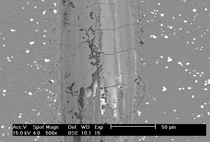
6 Laser Drilled Ceramic HAZ HAZ Boundary Molten/solidified ceramic Chip out at the top of the via due to molten ceramic cracking Cracking as molten ceramic region solidifies

7
8
9 Observations from Cross Sections Re-caste zone where molten ceramic resolidifies and cracks HAZ formation Cracking at HAZ/non HAZ interface


10 SEM Planar Photos of Top of Via Optical Photos of Top Surface for AlN Part Blisters
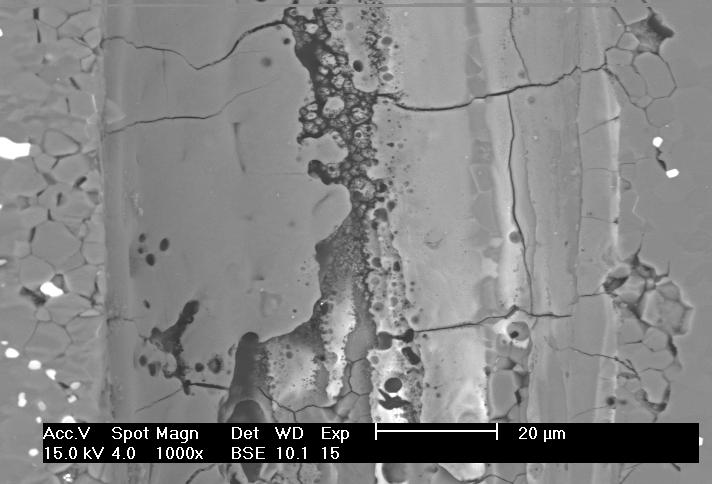
11 SEM Planar Photos of Top of Via after Vacuum Impregnation with Epoxy and Re-Polishing Wetted Y-Al-O Cracking in HAZ HAZ Boundary Drilling is thermal (melt/vaporize) vs. direct vaporization - Average power is too high - Peak power may be too low - Use shorter laser pulses if possible to increase peak power and decrease average power
12 SEM Planar Photos of Top of Via after Vacuum Impregnation with Epoxy and Re-Polishing Wetted Y-Al-O Cracking in HAZ
13 Why Process with Ultra-Short Pulses 10 femtosecond (10-14 seconds) to 10 nanoseconds (10-8 seconds) which includes the picosecond regime Very high peak power, very low average power Drill without heat and without melting the substrate using cold ablation Substrate material is directly converted into a plasma

 vs.")
14 Threshold of laser pulse energy to create plasma (ablation drilling) vs. thermal drilling

15 No heat transfer to surrounding materialà NO HAZ FORMATION AND NO CRACKING AT HAZ/ NON HAZ INTERFACE No melting or vaporizing of substrate à NO SLAG ON SURFACE OR WITHIN THE VIA Key sacrifice for improved quality à LOWER DRILLING SPEED

16 Laser Drill with NO HEAT
17 Examples of Materials Drilled with Picosecond Pulses

18 Drilling Stainless Steel
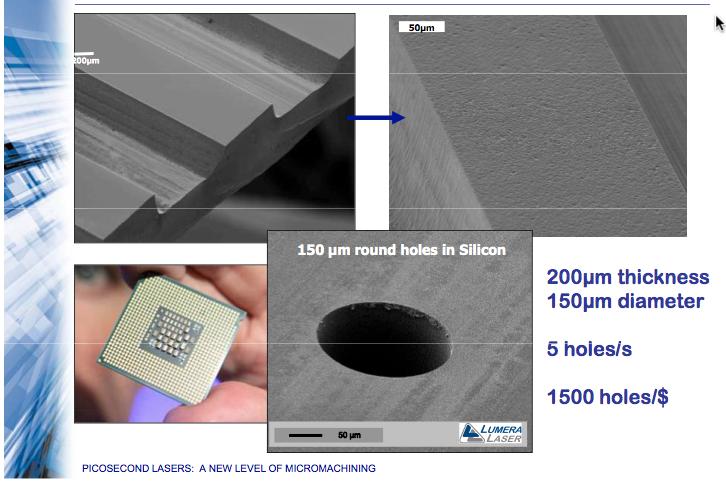
19 Silicon
20 Picosecond Laser Systems
21 Picosecond Laser Characteristics

22 Thin Disc Lasers Gain medium is a thin disc (typically Yb doped YAG Crystal) Attached to a heat sink for very efficient heat removal Pumped with a diode laser
23 Pump Laser incident on Yb:YAG disc to provide energy


24 Crystal Oscillator driven by RF signal inserted in laser cavity. Only certain laser mode are now supported by the cavity, a condition called mode locked. This results in a laser output of a stream of short pulses.
25 Pulsed laser output is followed by Pulse Selection and Amplifier(s)

26 Picosecond Laser Characteristics
27 Comparison with Longer Pulse Drilling

28 Optimum Range: ps Thermal Drilling Effects Peak powers so high that nonlinear optical effects start to occur
29 Shorter Pulses- Longer Drill Times (for Fixed Frequency and Pulse Energy) In this example: 20 ns is 1 µm/pulse 100 ns is 7 µm/pulse
30 Summary Picosecond pulse width => optimum for hole quality Cold ablation with minimal thermal effects Minimize: slag, HAZ formation, cracking at HAZ interface Trade off with slower drilling speed Material removal per pulse scale with pulse energy Shorter pulse, higher peak energy, lower pulse energy 50W ps laser could be 10x slower than CO2 laser at same frequency
Optical Components: Laser Crystals
 Optical Components: Laser Crystals Table of Contents Crystals Introduction... 2 Nd: YVO 4... 3 Nd:YAG... 6 Nd:YLF... 7 Cr:YAG... 9 1 Crystals Introduction Sinoceramics supplies many types of crystals for
Enabling Technology in Thin Wafer Dicing
 Enabling Technology in Thin Wafer Dicing Jeroen van Borkulo, Rogier Evertsen, Rene Hendriks, ALSI, platinawerf 2G, 6641TL Beuningen Netherlands Abstract Driven by IC packaging and performance requirements,
PDF created with FinePrint pdffactory Pro trial version
 Benefits Damage-free dicing of thin silicon Capable of producing smallest street widths which in return provides additional space for more parts per wafer Single step process results in reduction of cost
3 Pulsed laser ablation and etching of fused silica
 3 Pulsed laser ablation and etching of fused silica 17 3 Pulsed laser ablation and etching of fused silica Material erosion caused by short laser pulses takes place far from equilibrium and may be based
Lasers and Laser Systems for Micro-machining
 Lasers and Laser Systems for Micro-machining Martyn Knowles Oxford Lasers Ltd Unit 8, Moorbrook Park Didcot, Oxfordshire, OX11 7HP Tel: +44 (0) 1235 810088 www.oxfordlasers.com Lasers and Laser Systems
Thermal Evaporation. Theory
 Thermal Evaporation Theory 1. Introduction Procedures for depositing films are a very important set of processes since all of the layers above the surface of the wafer must be deposited. We can classify
High Power Operation of Cryogenic Yb:YAG. K. F. Wall, B. Pati, and P. F. Moulton Photonics West 2007 San Jose, CA January 23, 2007
 High Power Operation of Cryogenic Yb:YAG K. F. Wall, B. Pati, and P. F. Moulton Photonics West 2007 San Jose, CA January 23, 2007 Outline Early work on cryogenic lasers MPS laser technology Recent program
11.3 Polishing with Laser Radiation
 196 E. Willenborg 11.3 Polishing with Laser Radiation Edgar Willenborg The surface roughness of a part or product strongly influences its properties and functions. Among these can be counted abrasion and
Laser Micromachining of Bulk Substrates and Thin Films Celine Bansal
 Laser Micromachining of Bulk Substrates and Thin Films Celine Bansal Oxford Lasers Ltd Moorbrook Park Didcot, Oxfordshire, OX11 7HP Tel: +44 (0) 1235 810088 www.oxfordlasers.com Outline Oxford Lasers Importance
LOW TEMPERATURE PHOTONIC SINTERING FOR PRINTED ELECTRONICS. Dr. Saad Ahmed XENON Corporation November 19, 2015
 LOW TEMPERATURE PHOTONIC SINTERING FOR PRINTED ELECTRONICS Dr. Saad Ahmed XENON Corporation November 19, 2015 Topics Introduction to Pulsed Light Photonic sintering for Printed Electronics R&D Tools for
TruMicro: Power meets precision. Machine tools / Power tools Laser technology / Electronics
 TruMicro: Power meets precision. Machine tools / Power tools Laser technology / Electronics Great results on a small scale. Contents Great results on a small scale. 2 Cold material processing. 4 Our expertise
PULSED LASER WELDING
 PULSED LASER WELDING Girish P. Kelkar, Ph.D. Girish Kelkar, Ph.D, WJM Technologies, Cerritos, CA 90703, USA Laser welding is finding growing acceptance in field of manufacturing as price of lasers have
Fabrication of the Crystalline ITO Pattern by Picosecond Laser with a Diffractive Optical Element
 Fabrication of the Crystalline ITO Pattern by Picosecond Laser with a Diffractive Optical Element C.W. Chien and C.W. Cheng* ITRI South Campus, Industrial Technology Research Institute, No. 8, Gongyan
Qswitched lasers are gaining more interest because of their ability for various applications in remote sensing, environmental monitoring, micro
 90 Qswitched lasers are gaining more interest because of their ability for various applications in remote sensing, environmental monitoring, micro machining, nonlinear frequency generation, laserinduced
High Transmittance Ti doped ITO Transparent Conducting Layer Applying to UV-LED. Y. H. Lin and C. Y. Liu
 High Transmittance Ti doped ITO Transparent Conducting Layer Applying to UV-LED Y. H. Lin and C. Y. Liu Department of Chemical Engineering and Materials Engineering, National Central University, Jhongli,
Challenges and Future Directions of Laser Fuse Processing in Memory Repair
 Challenges and Future Directions of Laser Fuse Processing in Memory Repair Bo Gu, * T. Coughlin, B. Maxwell, J. Griffiths, J. Lee, J. Cordingley, S. Johnson, E. Karagiannis, J. Ehrmann GSI Lumonics, Inc.
High Throughput Laser Processing of Guide Plates for Vertical Probe Cards Rouzbeh Sarrafi, Dana Sercel, Sean Dennigan, Joshua Stearns, Marco Mendes
 High Throughput Laser Processing of Guide Plates for Vertical Probe Cards Rouzbeh Sarrafi, Dana Sercel, Sean Dennigan, Joshua Stearns, Marco Mendes IPG Photonics - Microsystems Division Outline Introduction
Laser damage threshold of AR coatings on phosphate glass
 Laser damage threshold of AR coatings on phosphate glass Optical Coatings for Laser Applications Wednesday, 12 th April 2017, Buchs SG, Switzerland dirk.apitz@schott.com, SCHOTT Suisse SA, Advanced Optics,
Laser grooving technique for dicing nanoscale low-k wafer
 Laser grooving technique for dicing nanoscale low-k wafer Hsiang-Chen Hsu and Shih-Jeh Wu Professor Department of Mechanical and Automation Engineering I-Shou University HCHSU, ISU/Slide 1 Outline Background
Laser Material Processing New Frontiers New Opportunities Terry VanderWert/ Prima Power Laserdyne
 Laser Material Processing New Frontiers New Opportunities Terry VanderWert/ Prima Power Laserdyne Moving the frontier from solution looking for a problem to enabling technology 2 About Prima Power Laserdyne
Modern Methods of Surface Engineering
 LVIV POLYTECHNIC NATIONAL UNIVERSITY Modern Methods of Surface Engineering Institute of Engineering Mechanics and Transport Department of Applied Materials Science and Materials Engineering Asssistant
AILU Technology Workshop
 AILU Technology Workshop Welding of metals using high power fiber delivered diode laser beams Dipl.-Ing. Mark Daichendt Laserline GmbH Mülheim-Kärlich Germany www.laserline.de 1 Outline Laserline company
Optimizing the processing of sapphire with ultrashort laser pulses
 Optimizing the processing of sapphire with ultrashort laser pulses Geoff Lott 1, Nicolas Falletto 1, Pierre-Jean Devilder, and Rainer Kling 3 1 Electro Scientific Industries, Eolite Systems, 3 Alphanov
In-process Monitoring and Adaptive Control during Micro Welding with CW Fiber Laser
 In-process Monitoring and Adaptive Control during Micro Welding with CW Fiber Laser Yousuke KAWAHITO*, Masaharu KAWASAKI* and Seiji KATAYAMA* * Osaka University, Joining and Welding Research Institute
Chapter 3 Silicon Device Fabrication Technology
 Chapter 3 Silicon Device Fabrication Technology Over 10 15 transistors (or 100,000 for every person in the world) are manufactured every year. VLSI (Very Large Scale Integration) ULSI (Ultra Large Scale
Isolation Scribing on Hybrid Films for CIGS-Based Solar Cell Using Various Nanosecond Pulsed Laser Wavelengths
 Isolation Scribing on Hybrid Films for CIGS-Based Solar Cell Using Various Nanosecond Pulsed Laser Wavelengths Ming-Fei Chen *, Wen-Tse Hsiao **, Ming-Cheng Wang * and Ying-Fang Chen * * Department of
Introduction. 1. Sputtering process, target materials and their applications
 Sputtering is widely used in the production of electronic devices such as liquid crystal displays (LCDs), optical media, magnetic media and semiconductors. The Kobelco Research Institute, Inc. has been
Improving Laser Ablation of Zirconia by Liquid Films: Multiple Influence of Liquids on Surface Machining and Nanoparticle Generation
 Improving Laser Ablation of Zirconia by Liquid Films: Multiple Influence of Liquids on Surface Machining and Nanoparticle Generation Niko BÄRSCH *1, Antonietta GATTI *2, and Stephan BARCIKOWSKI *1 *1 Laser
SUPERPULSE : A NANOSECOND PULSE FORMAT FOR IMPROVING LASER DRILLING
 GA A25867 SUPERPULSE : A NANOSECOND PULSE FORMAT FOR IMPROVING LASER DRILLING by A.C. FORSMAN, E.H. LUNDGREN, A.L. DODELL, A.M. KOMASHKO, and M.S. ARMAS JUNE 2007 QTYUIOP DISCLAIMER This report was prepared
In-Process Monitoring and Adaptive Control in Micro Welding with a Single-Mode Fiber Laser.
 Title Author(s) In-Process Monitoring and Adaptive Control in Micro Welding with a Single-Mode Fiber Laser KAWAHITO, Yousuke; KATAYAMA, Seiji Citation Transactions of JWRI. 38(2) P.5-P.11 Issue Date 2009-12
A New Thermal Management Material for HBLEDs based on Aluminum Nitride Ceramics
 A New Thermal Management Material for HBLEDs based on Aluminum Nitride Ceramics Thermal Management Challenges in HBLED Excess heat leads to a whole range of performance and reliability issues for high
Device Fabrication: Metallization
 Device Fabrication: Metallization 1 Applications: Interconnection 2 Q & A Can we reduce all dimensions of metal interconnection line at the same ratio? R= l/wh. When we shrink all dimensions (length l,
Advances in Intense Pulsed Light Solutions For Display Manufacturing. XENON Corporation Dr. Saad Ahmed Japan IDW 2016
 Advances in Intense Pulsed Light Solutions For Display Manufacturing XENON Corporation Dr. Saad Ahmed Japan IDW 2016 Talk Outline Introduction to Pulsed Light Applications in Display UV Curing Applications
TruMicro: Power meets precision. Machine tools / Power tools Laser technology / Electronics
 TruMicro: Power meets precision. Machine tools / Power tools Laser technology / Electronics Great results on a small scale. Contents Great results on a small scale. 2 Cold material processing. 4 Our expertise
Trench Structure Improvement of Thermo-Optic Waveguides
 International Journal of Applied Science and Engineering 2007. 5, 1: 1-5 Trench Structure Improvement of Thermo-Optic Waveguides Fang-Lin Chao * Chaoyang University of Technology, Wufong, Taichung County
Excimer Laser Annealing of Hydrogen Modulation Doped a-si Film
 Materials Transactions, Vol. 48, No. 5 (27) pp. 975 to 979 #27 The Japan Institute of Metals Excimer Laser Annealing of Hydrogen Modulation Doped a-si Film Akira Heya 1, Naoto Matsuo 1, Tadashi Serikawa
INTRODUCTION. Think HSS
 INTRODUCTION Think HSS SUMMARY METALLURGY 2 Excellent strength 3 A super sharp edge 4 Safe and reliable tools Alloy elements 6 The influence of alloy elements 7 Standard compositions of HSS 8 The HSS-PM
Damage Threats and Response of Final Optics for Laser-Fusion Power Plants
 Damage Threats and Response of Final Optics for Laser-Fusion Power Plants M. S. Tillack 1, S. A. Payne 2, N. M. Ghoniem 3, M. R. Zaghloul 1 and J. F. Latkowski 2 1 UC San Diego, La Jolla, CA 92093-0417
Laser Dicing of Silicon: Comparison of Ablation Mechanisms with a Novel Technology of Thermally Induced Stress
 Dicing of Silicon: Comparison of Ablation Mechanisms with a Novel Technology of Thermally Induced Stress Oliver HAUPT, Frank SIEGEL, Aart SCHOONDERBEEK, Lars RICHTER, Rainer KLING, Andreas OSTENDORF Zentrum
Die Hardfacing and Remanufacturing using Direct Metal Deposition (DMD) B. Dutta POM Group, Inc., Auburn Hills, MI-48326
 B. Dutta POM Group, Inc., Auburn Hills, MI-48326") Die Hardfacing and Remanufacturing using Direct Metal Deposition (DMD) B. Dutta POM Group, Inc., Auburn Hills, MI-48326 OUTLINE Company Overview of Direct Metal Deposition DMD Systems DMD Application in
Die Hardfacing and Remanufacturing using Direct Metal Deposition (DMD) B. Dutta POM Group, Inc., Auburn Hills, MI-48326 OUTLINE Company Overview of Direct Metal Deposition DMD Systems DMD Application in
Microwave Plasma Processing
 Microwave Plasma Processing MUEGGE GMBH Hochstraße 4-6 64385 Reichelsheim Fon +49 (0) 6164-93 07 11 Fax +49 (0) 6164-93 07 93 info@muegge.de www.muegge.de Microwave Plasma Processing Microwave Plasma Technology:
Confocal Microscopy of Electronic Devices. James Saczuk. Consumer Optical Electronics EE594 02/22/2000
 Confocal Microscopy of Electronic Devices James Saczuk Consumer Optical Electronics EE594 02/22/2000 Introduction! Review of confocal principles! Why is CM used to examine electronics?! Several methods
Experiences of PLD Technology for LIB Separators. PICODEON Oy. Neal White
 Experiences of PLD Technology for LIB Separators PICODEON Oy Neal White 1 Outline Introduction to Picodeon Ceramic coating rationale Separator overview Why PLD for LIB separators Current status of Picodeon
Ceramic and glass technology
 1 Row materials preperation Plastic Raw materials preperation Solid raw materials preperation Aging wet milling mastication Mixing seving Grain size reduction Milling Crushing Very fine milling Fine milling
Sheet) Graphite Sheet
 Graphite Sheet") PGS(Pyrolytic Graphite Sheet) Graphite Sheet Panasonic Electronic Device Co.,Ltd Panasonic Electronic Device Hokkaido Co.,Ltd PGS Graphite Sheet PGS (Pyrolytic Highly Oriented Graphite Sheet) is made of
PGS(Pyrolytic Graphite Sheet) Graphite Sheet Panasonic Electronic Device Co.,Ltd Panasonic Electronic Device Hokkaido Co.,Ltd PGS Graphite Sheet PGS (Pyrolytic Highly Oriented Graphite Sheet) is made of
Effects of Laser Peening Parameters. on Plastic Deformation in Stainless Steel
 Effects of Laser Peening Parameters on Plastic Deformation in Stainless Steel Miho Tsuyama* 1, Yasuteru Kodama* 2, Yukio Miyamoto* 2, Ippei Kitawaki* 2, Masahiro Tsukamoto* 3 and Hitoshi Nakano* 1 *1 Faculty
Microstructuring of Steel and Hard Metal using Femtosecond Laser Pulses
 Available online at www.sciencedirect.com Physics Procedia 12 (2011) 60 66 LiM 2011 Microstructuring of Steel and Hard Metal using Femtosecond Laser Pulses Manuel Pfeiffer a *, Andy Engel a, Steffen Weißmantel
TECHNICAL GUIDE CUTTING
 TECHNICAL GUIDE CUTTING INTRODUCING OUR NEW PRODUCT NOMENCLATURE Bisalloy Steels has recently introduced a new product nomenclature. The following table details the grade equivalents. Note: Only the designation
Micro processing with laser radiation
 Micro processing with laser radiation Trends and perspectives Miniaturization and highly integrated functionalization are the driving factors in the production of innovative products in almost every industrial
Basics of Solar Photovoltaics. Photovoltaics (PV) Lecture-21
 Lecture-21") Lecture-21 Basics of Solar Photovoltaics Photovoltaics (PV) Photovoltaics (PV) comprise the technology to convert sunlight directly into electricity. The term photo means light and voltaic, electricity.
Lecture-21 Basics of Solar Photovoltaics Photovoltaics (PV) Photovoltaics (PV) comprise the technology to convert sunlight directly into electricity. The term photo means light and voltaic, electricity.
Cladding with High Power Diode Lasers
 White Paper Cladding with High Power Diode Lasers Cladding is a well established process used in a variety of industries for improving the surface and near surface properties (e.g. wear, corrosion or heat
Durability Testing of Ceramic Coatings for Indirect Resistance Heat Treating in Vehicle Lightweighting Applications
 Durability Testing of Ceramic Coatings for Indirect Resistance Heat Treating in Vehicle Lightweighting Applications Warren Peterson and Jerry E. Gould EWI Abstract The need for vehicle lightweighting has
The Many Facets and Complexities of 316L and the Effect on Properties
 The Many Facets and Complexities of 316L and the Effect on Properties Ingrid Hauer Miller Höganäs AB, Höganäs, Sweden state and country Ingrid.hauer@hoganas.com, +46702066244 Abstract One of the most widely
Introduction. Online course on Analysis and Modelling of Welding. G. Phanikumar Dept. of MME, IIT Madras
 Introduction Online course on Analysis and Modelling of Welding G. Phanikumar Dept. of MME, IIT Madras Classification of Manufacturing Processes Manufacturing Processes Ingot Casting Shape Casting Power
Surface Coating of Tungsten Carbide by Electric Exploding of Contact
 Surface Coating of Tungsten Carbide by Electric Exploding of Contact Evgeny G. Grigoryev General Physics Department, Moscow Engineering Physics Institute, Kashirskoe sh. 31, Moscow, 115409, Russia Abstract.
2.1 µm CW Raman Laser in GeO 2 Fiber
 2.1 µm CW Raman Laser in GeO 2 Fiber B. A. Cumberland, S. V. Popov and J. R. Taylor Femtosecond Optics Group, Imperial College London, SW7 2AZ, United Kingdom O. I. Medvedkov, S. A. Vasiliev, E. M. Dianov
Yung-Hui Yeh, and Bo-Cheng Kung Display Technology Center (DTC), Industrial Technology Research Institute, Hsinchu 310, Taiwan
, Industrial Technology Research Institute, Hsinchu 310, Taiwan") Amorphous In 2 O 3 -Ga 2 O 3 -ZnO Thin Film Transistors and Integrated Circuits on Flexible and Colorless Polyimide Substrates Hsing-Hung Hsieh, and Chung-Chih Wu* Graduate Institute of Electronics Engineering,
Amorphous In 2 O 3 -Ga 2 O 3 -ZnO Thin Film Transistors and Integrated Circuits on Flexible and Colorless Polyimide Substrates Hsing-Hung Hsieh, and Chung-Chih Wu* Graduate Institute of Electronics Engineering,
IMPACT DAMAGE DETECTION ON SCARF-REPAIRED COMPOSITES USING LAMB WAVE SENSING
 16 TH INTERNATIONAL CONFERENCE ON COMPOSITE MATERIALS IMPACT DAMAGE DETECTION ON SCARF-REPAIRED COMPOSITES USING LAMB WAVE SENSING Ichiya Takahashi*, Yusaku Ito*, Shin-ichi Takeda**, Yutaka Iwahori**,
Development of New Grade SUMIBORON BN7000 for Cast Iron and Ferrous Powder Metal Machining
 SPECIAL ISSUE Development of New SUMIBORON for Cast Iron and Ferrous Powder Metal Machining Yusuke Matsuda*, Katsumi OKaMura, shinya uesaka and tomohiro FuKaYa SUMIBORON P (polycrystalline cubic boron
Realisation d'un laser int6gr6 continu sur Nd:LiTaOs
 JOURNAL DE PHYSIQUE IV Colloque C4, supplkment au Journal de Physique 111, Volume 4, avril1994 Realisation d'un laser int6gr6 continu sur Nd:LiTaOs S. NOUH, I? BALDI, M. DE MICHELI, G. MONNOM, D.B. OSTROWSKY,
FABRICATION AND RELIABILITY OF ULTRA-FINE RDL STRUCTURES IN ADVANCED PACKAGING BY EXCIMER LASER ABLATION
 FABRICATION AND RELIABILITY OF ULTRA-FINE RDL STRUCTURES IN ADVANCED PACKAGING BY EXCIMER LASER ABLATION NCCAVS Joint Users Group Technical Symposium San Jose, June 7 th, 2017 Markus Arendt, SÜSS MicroTec
Leveraging the Precision of Electroforming over Alternative Processes When Developing Nano-scale Structures
 VOLUME 4 - ELECTROFORMING Leveraging the Precision of over Alternative Processes When Developing Nano-scale Structures Electrical and mechanical component and subsystem designers generally have five techniques
Laser assisted Cold Spray
 2009-02-16 Laser assisted Cold Spray Andrew Cockburn, Matthew Bray, Rocco Lupoi Bill O Neill Innovative Manufacturing Research Centre (IMRC) Institute for Manufacturing, Department of Engineering, University
>10 11 ohm-cm. ε T 11/ε0=6.7, ε T 33/ε0=8.1; Tan δ<0.001
 Beta-Barium Borate Crystal BBO Beta-Barium Borate (β-bab2o4 or BBO) is one of the most excellent NLO crystals. Using a newly improved flux method, AOTK now produces highquality BBO crystal with high optical
Abstract. Introduction
 Accelerating Silicon Carbide Power Electronics Devices into High Volume Manufacturing with Mechanical Dicing System By Meng Lee, Director, Product Marketing and Jojo Daof, Senior Process Engineer Abstract
FABRICATION ENGINEERING MICRO- NANOSCALE ATTHE AND. Fourth Edition STEPHEN A. CAMPBELL. of Minnesota. University OXFORD UNIVERSITY PRESS
 AND FABRICATION ENGINEERING ATTHE MICRO- NANOSCALE Fourth Edition STEPHEN A. CAMPBELL University of Minnesota New York Oxford OXFORD UNIVERSITY PRESS CONTENTS Preface xiii prrt i OVERVIEW AND MATERIALS
Alternative Methods of Yttria Deposition For Semiconductor Applications. Rajan Bamola Paul Robinson
 Alternative Methods of Yttria Deposition For Semiconductor Applications Rajan Bamola Paul Robinson Origin of Productivity Losses in Etch Process Aggressive corrosive/erosive plasma used for etch Corrosion/erosion
Ultra High Barrier Coatings by PECVD
 Society of Vacuum Coaters 2014 Technical Conference Presentation Ultra High Barrier Coatings by PECVD John Madocks & Phong Ngo, General Plasma Inc., 546 E. 25 th Street, Tucson, Arizona, USA Abstract Silicon
Available online at ScienceDirect. Physics Procedia 56 (2014 ) Ultra-short pulse laser structuring of molding tools
 Ultra-short pulse laser structuring of molding tools") Available online at www.sciencedirect.com ScienceDirect Physics Procedia 56 (2014 ) 1041 1046 8 th International Conference on Photonic Technologies LANE 2014 Ultra-short pulse laser structuring of molding
Available online at www.sciencedirect.com ScienceDirect Physics Procedia 56 (2014 ) 1041 1046 8 th International Conference on Photonic Technologies LANE 2014 Ultra-short pulse laser structuring of molding
Marking Decorative Features to Stainless Steel with Fiber Laser
 Marking Decorative Features to Stainless Steel with Fiber Laser Petri Laakso, Ville Mehtälä VTT Technical Research Centre of Finland Henrikki Pantsar Fraunhofer Color marking on stainless steel has been
SUSS SOLUTIONS FOR LARGE FORMAT PATTERNING UV Scanning Lithography and Excimer Laser Ablation
 SUSS SOLUTIONS FOR LARGE FORMAT PATTERNING UV Scanning Lithography and Excimer Laser Ablation Kevin Yang, Habib Hichri, Ralph Zoberbier SÜSS MicroTec Photonic Systems Inc. June 18, 2015 MARKET DRIVER Mobile
Project III. 4: THIN FILM DEVICES FOR LARGE AREA ELECTRONICS
 Project III. 4: THIN FILM DEVICES FOR LARGE AREA ELECTRONICS Project leader: Dr D.N. Kouvatsos Collaborating researchers from other projects: Dr D. Davazoglou Ph.D. candidates: M. Exarchos, L. Michalas
Evaluation of Bubblers and Baffles for Cooling of Die Casting Dies
 NADCA Die Materials Committee Evaluation of Bubblers and Baffles for Cooling of Die Casting Dies John F. Wallace David Schwam Sun Feng Sebastian Birceanu Case Western Reserve University Cleveland, OH -
Fraunhofer ENAS Current results and future approaches in Wafer-level-packaging FRANK ROSCHER
 Fraunhofer ENAS - Current results and future approaches in Wafer-level-packaging FRANK ROSCHER Fraunhofer ENAS Chemnitz System Packaging Page 1 System Packaging Outline: Wafer level packaging for MEMS
Index. Automotive engines, silicon nitride products development, 83-94
 Index Advanced composite ceramics, properties and applications, 109-22 Aircraft engine bearings, shaft speed limits, 46-8 Alumina cast sintered, applications, 72-5 comparative erosive wear performance,
NanoSystemsEngineering: NanoNose Final Status, March 2011
 1 NanoSystemsEngineering: NanoNose Final Status, March 2011 The Nanonose project is based on four research projects (VCSELs, 3D nanolithography, coatings and system integration). Below, the major achievements
Femtosecond Laser Materials Processing
 Preprint UCRL-JC-126901 Rev 4 Femtosecond Laser Materials Processing P. S. Banks, B. C. Stuarf, A. M. Komashko, M. D. Feit, A. M. Rubenchik, and M. D. Perry This article was submitted to Photonics West
Effects of Pulsed Laser Micro Polishing on Microstructure and Mechanical Properties of S7 Tool Steel
 Effects of Pulsed Laser Micro Polishing on Microstructure and Mechanical Properties of S7 Tool Steel ICOMM 2014 No. 103 Justin D. Morrow 1, Qinghua Wang 2, Neil A. Duffie 3, Frank E. Pfefferkorn 4 1 Justin
Cu/synthetic and impact-diamond composite heatconducting
 Journal of Physics: Conference Series PAPER OPEN ACCESS Cu/synthetic and impact-diamond composite heatconducting substrates To cite this article: E N Galashov et al 2016 J. Phys.: Conf. Ser. 690 012043
Optical Coatings. Photonics 4 Luxury Coatings , Genève. Dr. Andreas Bächli Head of Optical Coatings at RhySearch, Buchs (SG)
") Optical Coatings Photonics 4 Luxury Coatings 21.06.2017, Genève Dr. Andreas Bächli Head of Optical Coatings at RhySearch, Buchs (SG) RhySearch The Research- and Innovation Center in the Rhine Valley RhySearch
Optical Coatings Photonics 4 Luxury Coatings 21.06.2017, Genève Dr. Andreas Bächli Head of Optical Coatings at RhySearch, Buchs (SG) RhySearch The Research- and Innovation Center in the Rhine Valley RhySearch
BBO Crystals. Features. Broad phase-matchable second-harmonic-generation (SHG) range from nm to 2500 nm
 range from nm to 2500 nm") BBO Crystals Broad phase-matchable second-harmonic-generation (SHG) range from 409.6 nm to 2500 nm Wide transparency range from 189 nm to 2600 nm High damage threshold of 10 J/cm 2 for 10 ns pulse-width
BBO Crystals Broad phase-matchable second-harmonic-generation (SHG) range from 409.6 nm to 2500 nm Wide transparency range from 189 nm to 2600 nm High damage threshold of 10 J/cm 2 for 10 ns pulse-width
EE 330 Lecture 9. IC Fabrication Technology Part II. -Oxidation -Epitaxy -Polysilicon -Planarization -Resistance and Capacitance in Interconnects
 EE 330 Lecture 9 IC Fabrication Technology Part II -Oxidation -Epitaxy -Polysilicon -Planarization -Resistance and Capacitance in Interconnects Review from Last Time Etching Dry etch (anisotropic) SiO
LOT. Contents. Introduction to Thin Film Technology. Chair of Surface and Materials Technology
 Introduction to Thin Film Contents 1. Introduction and Application Examples (2h) 2. Preparation of Thin Films by PVD (Physical Vapor Deposition) (6h) 2.1 Vacuum Technique (1h) 2.1.1 Kinetics of Gases 2.1.2
MODELING OF LASER BASED DIRECT METAL DEPOSITION PROCESS
 MODELING OF LASER BASED DIRECT METAL DEPOSITION PROCESS Jayanth N PG Student PSG College of Technology jayanthnagaraj@gmail.com Ravi K R Associate Professor PSG College of Technology Krravi.psgias@gmail.com
I IRRI
 THE AMERICAN SOCIETY OF MECHANICAL ENGINEERS Three Park Avenue, New York, N.Y. 10016-6990 99-GT-417 The Society shall not be responsible for statements or opinions advanced In papers or discuszo311 at
Issue 51 September 2013
 Laser Decapsulation By Christopher Henderson Historically, failure analysts used either mechanical or chemical means to decapsulate integrated circuits. They used primarily mechanical means on hermetically-sealed
Characterization of laser-material interaction during laser cladding process P.-A. Vetter,* J. Fontaine,* T. Engel," L. Lagrange,& T.
 Characterization of laser-material interaction during laser cladding process P.-A. Vetter,* J. Fontaine,* T. Engel," L. Lagrange,& T. Marchione^ f^, BID de /a rzcfozre ^7000 France ABSTRACT The interaction
Pulsed Laser Assisted Micromilling for Die/Mold Manufacturing
 Pulsed Laser Assisted Micromilling for Die/Mold Manufacturing Tuğrul Özel* Dept. of Industrial and Systems Engineering Rutgers University Piscataway, NJ 08854 USA ozel@rci.rutgers.edu *Corresponding author
Annealing Effect on Elastic Constant of Ultrathin Films Studied by Acoustic-Phonon Resonance Spectroscopy
 1st International Symposium on Laser Ultrasonics: Science, Technology and Applications July 16-18 28, Montreal, Canada Annealing Effect on Elastic Constant of Ultrathin Films Studied by Acoustic-Phonon
3D technologies for integration of MEMS
 3D technologies for integration of MEMS, Fraunhofer Institute for Electronic Nano Systems Folie 1 Outlook Introduction 3D Processes Process integration Characterization Sample Applications Conclusion Folie
FIVE STAR PRODUCTS, INC. (800)
") FIVE STAR PRODUCTS, INC. www.fivestarproducts.com (800) 243-2206 Page 1 of 11 DESIGN-A-SPEC GUIDELINES FIVE STAR RS ANCHOR GEL CONTENTS PART A - GENERAL CONDITIONS PART B - MATERIAL SPECIFICATIONS PART
FIVE STAR PRODUCTS, INC. www.fivestarproducts.com (800) 243-2206 Page 1 of 11 DESIGN-A-SPEC GUIDELINES FIVE STAR RS ANCHOR GEL CONTENTS PART A - GENERAL CONDITIONS PART B - MATERIAL SPECIFICATIONS PART
Transparent Ceramic Yb 3+ :Lu2O3 Materials
 Contract no.: FA2386-10-1-4113 Final report for the project on: Transparent Ceramic Yb 3+ :Lu2O3 Materials Submission Date: Jan 19 th, 2012 Principal Investigator: Dr. Akio Ikesue World-Lab. Co., Ltd.
BONDING OF MULTIPLE WAFERS FOR HIGH THROUGHPUT LED PRODUCTION. S. Sood and A. Wong
 10.1149/1.2982882 The Electrochemical Society BONDING OF MULTIPLE WAFERS FOR HIGH THROUGHPUT LED PRODUCTION S. Sood and A. Wong Wafer Bonder Division, SUSS MicroTec Inc., 228 SUSS Drive, Waterbury Center,
J. B. Bates, Xiaohua Yu, C. F. Luck, and N. J. Dudney
 C/ORNL 90 0038 CRADA Final Report for CRADA Number ORNL90-0038 DEVELOPMENT OF A LITHIUM MICROBATTERY PACKAGING TECHNOLOGY ERKTSOl J. B. Bates, Xiaohua Yu, C. F. Luck, and N. J. Dudney Oak Ridge National
CHAPTER 4 APPLICATION OF SEMISOLID LUBRICANTS FOR IMPROVING RAKE FACE LUBRICATION 4.1 INTRODUCTION During minimal fluid application, since only a
 CHAPTER 4 APPLICATION OF SEMISOLID LUBRICANTS FOR IMPROVING RAKE FACE LUBRICATION 4.1 INTRODUCTION During minimal fluid application, since only a very small quantity of cutting fluid is used for the dual
Superconductors Processing and Equipment. Text Reference: Manufacturing Engineering and Technology, Kalpakjian & Schmid, 6/e, 2010 Chapter 18
 Ceramics, Glasses, Superconductors Processing and Equipment Text Reference: Manufacturing Engineering and Technology, g g g gy, Kalpakjian & Schmid, 6/e, 2010 Chapter 18 FIGURE 18.1 (a) Examples of typical
curamik CERAMIC SUBSTRATES AMB technology Design Rules Version #04 (09/2015)
") curamik CERAMIC SUBSTRATES AMB technology Design Rules Version #04 (09/2015) Content 1. Geometric properties 1.01. Available ceramic types / thicknesses... 03 1.02. thicknesses (standard)... 03 3. Quality
curamik CERAMIC SUBSTRATES AMB technology Design Rules Version #04 (09/2015) Content 1. Geometric properties 1.01. Available ceramic types / thicknesses... 03 1.02. thicknesses (standard)... 03 3. Quality
Fully Active Cooled In-vessel Components of EAST Tokamak
 1 FTP/P1-30 Fully Active Cooled In-vessel Components of EAST Tokamak Y.T. Song, X. Ji, G. Shen, T.J. Xu, Z.B. Zhou, L. Cao, X.F. Liu, W.W. Xu, X.B. Peng, S.M. Wang, P, Zhang, N. Zhu, J.F. Wu, D.M. Gao,
Application of Electronic Devices for Aerosol Deposition Methods
 Application of Electronic Devices for Aerosol Deposition Methods NAKADA Masafumi, KAWAKAMI Toshihiro, IWANAMI Mizuki, OHASHI Keishi Abstract Oxide materials have superior functional characteristics that