About Omics Group conferences
|
|
|
- Jeremy Fields
- 5 years ago
- Views:
Transcription
1 About Omics Group OMICS Group International through its Open Access Initiative is committed to make genuine and reliable contributions to the scientific community. OMICS Group hosts over 400 leading-edge peer reviewed Open Access Journals and organize over 300 International Conferences annually all over the world. OMICS Publishing Group journals have over 3 million readers and the fame and success of the same can be attributed to the strong editorial board which contains over eminent personalities that ensure a rapid, quality and quick review process.
2 About Omics Group conferences OMICS Group signed an agreement with more than 1000 International Societies to make healthcare information Open Access. OMICS Group Conferences make the perfect platform for global networking as it brings together renowned speakers and scientists across the globe to a most exciting and memorable scientific event filled with much enlightening interactive sessions, world class exhibitions and poster presentations Omics group has organised 500 conferences, workshops and national symposium across the major cities including SanFrancisco,Omaha,Orlado,Rayleigh,SantaClara,Chicag o,philadelphia,unitedkingdom,baltimore,sanantanio,dub ai,hyderabad,bangaluru and Mumbai.
3 Synthesis of nanometric iron oxide and chromium oxide films by reactive pulsed laser deposition for thermo sensors and thermo converters 1 S. A. Mulenko, 2 V.A.Nikirin, 3 N.Stefan 1 Institute for Metal Physics NAS of Ukraine, 36, Academician Vernadsky Blvd., UA-03142, Kiev-142, Ukraine; 2 V.F.Lashkaryov Vernadsky Blvd., UA-03142, Kiev-142, Ukraine; V.F.Lashkaryov Institute of Semiconductor Physics NAS of Ukraine, 41, Prospect Nauki, UA-03028, Kiev-28, Ukraine; 3 National Institute for Laser, Plasma and Radiation Physics, PO Box MG-54, RO-77125, Magurele, Romania.
4 Outline Introduction. Reactive Pulsed laser deposition (RPLD). Structural and electrical properties of nanometric iron oxide and chromium oxide films Thermo sensors and thermo converters. Conclusions.
5
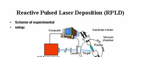
6
7 Structural and electrical properties : thermo e.m.f. coefficient (S) measurement Experimental scheme: T 1 T 2 S= V/ T T = T 1 -T 2 V Heater Substrate Film
8 Deposition of nanometric -x films by RPLD 1,6 ln[σ(t 1 )/σ(t)] 1,4 1, ,0 0,8 0,6 1 0,4 0,2 0,0 0, , , , , , , , /T, 1/K σ=σ g exp(-eg/2kt); Arrhenius plots of ln[σ(t 1 )/σ(t)] vs. 1/T. From the best fit of the experimental points the energy gap values Eg were calculated for films deposited at different oxygen pressure:1) p=0.05 Pa: Eg=0.43 ev; 2)p=0.1 Pa: Eg =0.70 ev; 3) p = 0.5 Pa: Eg=0.86 ev; 4)p=1.0 Pa: Eg=0.93 ev; Ts=293 K, N=4000. Eg = 2k ln[ σ( T1 )/ σ( T)] 1/ T 1/ T 1
9 XRD spectra of nanometric iron oxide films deposited on <100>Si substrate Intensity, a.u [012] [104] [202] [400] Si Intensity, a.u [214] 100 [012] [104] [110] O Fe 3 2 [113] [024] [400] Si [116] [214] O Fe 3 2 [1010] Θ Θ XRD spectra of -X (0 x 1) deposited on <100>Si substrate at O 2 pressure of 0.5 Pa in the chamber and the number of laser pulses (N)= 5000: left-substrate temperature 293 K; right-substrate temperature 800 K.
10 Iron oxide film thickness vs. the number of laser pulses (N) and O 2 pressure of 0.5 Pa in the chamber 40 d, nm T S =293 K; 2-T S = 800 K N
11 Thermo-electromotive force coefficient (S) vs. temperature for nanometric iron oxide films S, mv/k N=4000; N=5000; N=6000; PO 2 =0.5 Pa;T S =800 K; <100>Si; -X T, K
12 The figure of merit (ZT) vs. temperature for nanometric -X (0 x 1) films deposited by RPLD on Si substrate at PO 2 = 0.5 Pa, T S = 800 K, N = 5000, 6000 σ(ωxcm) T, K ZT N=5000; N=6000; T S =800 K;<100>Si; -X N=5000; N=6000; PO 2 =0.5 Pa; T S =800 K; <100>Si; -X T, K 2 T = ZT= σ ( S) χ χ χ + ; e l ; σ χ = L T χ e
13 Deposition of nanometric Cr 3-x -y films by RPLD 1,7 1,6 1,5 1,4 1,3 1,2 1,1 1,0 0,9 0,8 0,7 0,6 0,5 0,4 0,3 0,2 0,1 0,0 ln[σ(t 1 )σ/(t)] 0,0030 0,0031 0,0032 0,0033 0,0034 0, /T, 1/K 80 nm: Ω -1 cm -1 at K: Eg = 0.40 ev; 200 nm: Ω -1 cm -1 at K: Eg = 0.71 ev. Arhenius plot of ln[ σ(t 1 )/ σ (T) ] vs.1/t, wherefrom the energy band gap Eg was calculated for films deposited on <100>Si substrate at different oxygen pressure (P): 1- P = 0.05 Pa: Eg = (0.32 ± 0.03) ev; 2- P = 0.10 Pa: Eg = (0.40 ± 0.04) ev; 3 P = 1.0 Pa: Eg= (0.71 ± 0.07) ev; 4- P= 5 Pa;Eg= (0.38 ± 0.04)eV.N=4000, Ts=293K
14 XRD spectra of nanometric chromium oxide films deposited on <100>Si substrate [400] Si [400] Si Intensity, a. u [104] [110] [133] Cr CrO 2 Cr 3 PO 2 = 0.5 Pa; T S =293 K; N=4000; <100>Si Intensity, a. u [152] Cr [110] Cr [104] Cr 2 [041] [200] CrO3 3 Cr 3 O [152] [133] CrO CrO3 3 PaO 2 =0.5 O 2 ; T S =800Κ; N=4000;<100>Si Θ Θ XRD spectra of Cr 3-x -y (0 x 2; 0 y 2) film deposited on<100>si substrate at O 2 pressure of 0.5 Pa in the chamber and the number of laser pulses (N) = 4000 : left T S = 293 K; right T S = 800 K
15 Thermo-electromotive force coefficient (S) and the figure of merit (ZT) vs. temperature for nanometric chromium oxide films deposited on <100>Si substrate S, mv/k PaO 2 ; T S =800 K; N=4000; 0.5 PaO 2 ; T S =293 K; N=4000; Cr 3-X -Y ;<100>Si ZT Pa O 2 ; T S =293 K; 0.5 Pa O 2 ; T S =800 K; N=4000; Cr 3-X -Y ;<100>Si T, K T, K σ(ωxcm) T S = 800 K; T S = 293 K T, K
16 Conclusions The presented results show that RPLD can be used to produce nanometric iron oxide and chromium oxide films with polycrystalline structure variable thickness, variable degree of oxidation and variable band gap. The S coefficient and the figure of merit ZT for nanometric -x and Cr 3-x -y films deposited by RPLD demonstrated essentially higher values in comparison with other bulk or thin-film thermoelectric materials. These values strongly depend on deposition conditions. Nanometric iron and chromium oxide films, synthesized by UV photons using RPLD method, an exceptionally strong candidate for effective thermo sensors and thermo converters materials operating at moderate temperature.
17 Thank you for your attention!
18 Let Us Meet Again We welcome all to our future group conferences of Omics group international Please visit:
About Omics Group IBM Corporation. OMICS Group Conference - Philadelphia, PA 2014
 About Omics Group OMICS Group International through its Open Access Initiative is committed to make genuine and reliable contributions to the scientific community. OMICS Group hosts over 400 leading-edge
About Omics Group conferences
 About Omics Group OMICS Group International through its Open Access Initiative is committed to make genuine and reliable contributions to the scientific community. OMICS Group hosts over 400 leading-edge
Red luminescence from Si quantum dots embedded in SiO x films grown with controlled stoichiometry
 Red luminescence from Si quantum dots embedded in films grown with controlled stoichiometry Zhitao Kang, Brannon Arnold, Christopher Summers, Brent Wagner Georgia Institute of Technology, Atlanta, GA 30332
Department of Chemistry, University of California, Davis, California 95616, USA 2
 Enhance Solar Water Splitting Performance by Utilizing Near Infrared Radiation with Composite Films of Hematite and Rare Earth Doped Upconversion Materials Ming Zhang, 1 Yongjing Lin, 2 Thomas J. Mullen,
Preparation and characterization of nanostructured thermoelectric materials
 QuickTime et un décompresseur TIFF (non compressé) sont requis pour visionner cette image. Preparation and characterization of nanostructured thermoelectric materials Laboratoire de Physique des Matériaux,
Properties of Inclined Silicon Carbide Thin Films Deposited by Vacuum Thermal Evaporation
 182 Properties of Inclined Silicon Carbide Thin Films Deposited by Vacuum Thermal Evaporation Oday A. Hamadi, Khaled Z. Yahia, and Oday N. S. Jassim Abstract In this work, thermal evaporation system was
OMICS Group signed an agreement with more than International Societies to make healthcare informati on Open Access. OMICS Group Conferences
 About Omics Group OMICS Group International through its Open Ac cess Initiative is committed to make genuine an d reliable contributions to the scientific commu nity. OMICS Group hosts over 400 leading-edg
Supplementary Information
 Supplementary Information Formation of oxygen vacancies and Ti 3+ state in TiO 2 thin film and enhanced optical properties by air plasma treatment Bandna Bharti a, Santosh Kumar b, Heung-No Lee c and Rajesh
A NOVEL METHOD FOR THE IMPROVEMENT IN THERMOELECTRIC PROPERTY OF TIN OXIDE THIN FILMS AND ITS APPLICATION IN GAS SENSING
 INTERNATIONAL JOURNAL ON SMART SENSING AND INTELLIGENT SYSTEMS, VOL. 1, NO. 2, JUNE 2008 A NOVEL METHOD FOR THE IMPROVEMENT IN THERMOELECTRIC PROPERTY OF TIN OXIDE THIN FILMS AND ITS APPLICATION IN GAS
Solid-Phase Synthesis of Mg2Si Thin Film on Sapphire substrate
 Proc. Asia-Pacific Conf. on Semiconducting Silicides and Related Materials 2016 JJAP Conf. Proc. 5, https://doi.org/10.7567/jjapcp.5.011302 Solid-Phase Synthesis of Mg2Si Thin Film on Sapphire substrate
Influence of Annealing Temperature on the Properties of ITO Films Prepared by Electron Beam Evaporation and Ion-Assisted Deposition
 Kasetsart J. (Nat. Sci.) 42 : 362-366 (2008) Influence of Annealing Temperature on the Properties of ITO Films Prepared by Electron Beam Evaporation and Ion-Assisted Deposition Artorn Pokaipisit 1 *, Mati
Optical and Electrical Characterization of CuO Thin Films as Absorber Material for Solar Cell Applications
 American Journal of Condensed Matter Physics 16, 6(1): 1-6 DOI: 1.5923/j.ajcmp.11.1 Optical and Electrical Characterization of CuO Thin Films as Absorber Material for Solar Cell Applications K. S. Wanjala
Pulsed Laser Deposition of Epitaxial Titanium Nitride on Magnesium Oxide substrate
 Pulsed Laser Deposition of Epitaxial Titanium Nitride on Magnesium Oxide substrate By, Preetam ANBUKARASU UTRIP 2012 (1 st Crew) Under the Guidance of, Prof. Tetsuya HASEGAWA, Solid State Chemistry Lab,
Surfaces and Interfaces of Transparent Conducting Oxides Andreas Klein
 Surfaces and Interfaces of Transparent Conducting Oxides Andreas Klein Technische Universität Darmstadt, Institute of Materials Science, Surface Science Division Transparent conducting oxides d R T high
tion band derived electrons. Achieving high performance p-type oxide TFTswilldefinitelypromoteaneweraforelectronicsinrigidandflexible substrate away
 Preface Thin film transistor (TFT) is a combination of thin films necessary to create the function of a transistor. It consists of a thin film of a semiconducting material which forms the conducting channel
TFA Thin Film Analyzer
 TFA Thin Film Analyzer Thin Film Analyzer The LINSEIS Thin Film Analyzer is the perfect solution to characterize a broad range of thin film samples in a very comfortable and quick way. It is an easy to
Cluster-Assembled Nanophase (5 to 25 nm grains) Materials, Siegel, Annu. Rev. Mater. Sci. 21 (2991) 559.
 Materials, Siegel, Annu. Rev. Mater. Sci. 21 (2991) 559.") Cluster-Assembled Nanophase (5 to 25 nm grains) Materials, Siegel, Annu. Rev. Mater. Sci. 21 (2991) 559. Thermal evaporation of metals either in an inert gas or a reactive atmosphere. Metals, ceramics,
Cluster-Assembled Nanophase (5 to 25 nm grains) Materials, Siegel, Annu. Rev. Mater. Sci. 21 (2991) 559. Thermal evaporation of metals either in an inert gas or a reactive atmosphere. Metals, ceramics,
Materials Science for Achieving Green Innovation Thermoelectric Modules that Exploit Unutilized Heat for Revolutionizing Energy Conversion
 FEATURED ARTICLES Taking on Future Social Issues through Open Innovation Materials Science for Achieving Green Innovation Thermoelectric Modules that Exploit Unutilized Heat for Revolutionizing Energy
Kinetics of Silicon Oxidation in a Rapid Thermal Processor
 Kinetics of Silicon Oxidation in a Rapid Thermal Processor Asad M. Haider, Ph.D. Texas Instruments Dallas, Texas USA Presentation at the National Center of Physics International Spring Week 2010 Islamabad
International Journal of ChemTech Research CODEN (USA): IJCRGG ISSN: Vol.7, No.3, pp ,
: IJCRGG ISSN: Vol.7, No.3, pp ,") International Journal of ChemTech Research CDEN (USA): IJCRGG ISSN: 0974-4290 Vol.7, No.3, pp 1079-1084, 2014-2015 ICNN 2015 [4 th - 6 th Feb 2015] International ocnference on Nanoscience and Nanotechnology-2015
International Journal of ChemTech Research CDEN (USA): IJCRGG ISSN: 0974-4290 Vol.7, No.3, pp 1079-1084, 2014-2015 ICNN 2015 [4 th - 6 th Feb 2015] International ocnference on Nanoscience and Nanotechnology-2015
Structural and Optical Properties of MnO 2 : Pb Nanocrystalline Thin Films Deposited By Chemical Spray Pyrolysis
 IOSR Journal of Engineering (IOSRJEN) e-issn: 2250-3021, p-issn: 2278-8719 Vol. 3, Issue 4 (April. 2013), V4 PP 52-57 Structural and Optical Properties of MnO 2 : Pb Nanocrystalline Thin Films Deposited
Formation and Study of Properties of Ta and Mo Nanocluster Films
 MEPhI s Section of the Scientific Session on Breakthrough directions of scientific research at MEPhI: Development prospects within the Strategic Academic Units Volume 2018 Conference Paper Formation and
Electrical characteristics of Gd 2 O 3 thin film deposited on Si substrate
 Electrical characteristics of Gd 2 O 3 thin film deposited on Si substrate Chizuru Ohshima*, Ikumi Kashiwagi*, Shun-ichiro Ohmi** and Hiroshi Iwai* Frontier Collaborative Research Center* Interdisciplinary
Synthesis and Characterization of Zinc Iron Sulphide (ZnFeS) Of Varying Zinc Ion Concentration
 Of Varying Zinc Ion Concentration") International Journal of Science and Technology Volume 5 No. 5, May, 2016 Synthesis and Characterization of Zinc Iron Sulphide (ZnFeS) Of Varying Zinc Ion Concentration I. B. Obasi 1 and J. C. Osuwa 2
International Journal of Science and Technology Volume 5 No. 5, May, 2016 Synthesis and Characterization of Zinc Iron Sulphide (ZnFeS) Of Varying Zinc Ion Concentration I. B. Obasi 1 and J. C. Osuwa 2
Brochure Biotechnology World Convention
 Brochure Biotechnology World Convention Sao Paulo, Brazil August 15-17, 2016 Conference Secretariat 5716 Corsa Ave., Suite 110, West Lake, Los Angeles, CA 91362-7354, USA Ph: +1-650-268-9744, Fax: +1-650-618-1414,
Supplementary Figure S1 Photograph of MoS 2 and WS 2 flakes exfoliated by different metal naphthalenide (metal = Na, K, Li), and dispersed in water.
, and dispersed in water.") Supplementary Figure S1 Photograph of MoS 2 and WS 2 flakes exfoliated by different metal naphthalenide (metal = Na, K, Li), and dispersed in water. Supplementary Figure S2 AFM measurement of typical LTMDs
Supplementary Figure S1 Photograph of MoS 2 and WS 2 flakes exfoliated by different metal naphthalenide (metal = Na, K, Li), and dispersed in water. Supplementary Figure S2 AFM measurement of typical LTMDs
Summary and Scope for further study
 Chapter 6 Summary and Scope for further study 6.1 Summary of the present study Transparent electronics is an emerging science and technology field concentrated on fabricating invisible electronic circuits
Supporting Information
 Copyright WILEY-VCH Verlag GmbH & Co. KGaA, 69469 Weinheim, Germany, 2015. Supporting Information for Adv. Mater., DOI: 10.1002/adma.201500039 An Optoelectronic Resistive Switching Memory with Integrated
Combinatorial RF Magnetron Sputtering for Rapid Materials Discovery: Methodology and Applications
 Combinatorial RF Magnetron Sputtering for Rapid Materials Discovery: Methodology and Applications Philip D. Rack,, Jason D. Fowlkes, and Yuepeng Deng Department of Materials Science and Engineering University
This lecture is part of the Basic XRD Course.
 This lecture is part of the Basic XRD Course. Basic XRD Course 1 A perfect polycrystalline sample should contain a large number of crystallites. Ideally, we should always be able to find a set of crystallites
CHAPTER 5 Co-DOPED TiO 2 THIN FILMS: RESULTS AND DISCUSSION. 5.1 Introduction. 5.2 Effect of laser energy density (I)
") Chapter 5 Co-doped TiO 2 thin films results and discussion 81 CHAPTER 5 Co-DOPED TiO 2 THIN FILMS: RESULTS AND DISCUSSION 5.1 Introduction Thin films of Co-doped TiO 2 are used in a variety of optoelectronic
Chapter 5 Co-doped TiO 2 thin films results and discussion 81 CHAPTER 5 Co-DOPED TiO 2 THIN FILMS: RESULTS AND DISCUSSION 5.1 Introduction Thin films of Co-doped TiO 2 are used in a variety of optoelectronic
Influence of In/Sn ratio on nanocrystalline indium tin oxide thin films by spray pyrolysis method
 Available online at www.scholarsresearchlibrary.com Scholars Research Library Archives of Physics Research, 2011, 2 (1): 19-25 (http://scholarsresearchlibrary.com/archive.html) ISSN 0976-0970 CODEN (USA):
High Purity Chromium Metal Oxygen Distribution (Determined by XPS and EPMA)
") High Purity Chromium Metal Oxygen Distribution (Determined by XPS and EPMA) K. Suzuki, H. Tomioka To cite this version: K. Suzuki, H. Tomioka. High Purity Chromium Metal Oxygen Distribution (Determined
High Purity Chromium Metal Oxygen Distribution (Determined by XPS and EPMA) K. Suzuki, H. Tomioka To cite this version: K. Suzuki, H. Tomioka. High Purity Chromium Metal Oxygen Distribution (Determined
About OMICS Group Conferences
 About OMICS Group OMICS Group International is an amalgamation of Open Access publications and worldwide international science conferences and events. Established in the year 2007 with the sole aim of
Polycrystalline and microcrystalline silicon
 6 Polycrystalline and microcrystalline silicon In this chapter, the material properties of hot-wire deposited microcrystalline silicon are presented. Compared to polycrystalline silicon, microcrystalline
CHAPTER 4. SYNTHESIS OF ALUMINIUM SELENIDE (Al 2 Se 3 ) NANO PARTICLES, DEPOSITION AND CHARACTERIZATION
 NANO PARTICLES, DEPOSITION AND CHARACTERIZATION") 40 CHAPTER 4 SYNTHESIS OF ALUMINIUM SELENIDE (Al 2 Se 3 ) NANO PARTICLES, DEPOSITION AND CHARACTERIZATION 4.1 INTRODUCTION Aluminium selenide is the chemical compound Al 2 Se 3 and has been used as a precursor
40 CHAPTER 4 SYNTHESIS OF ALUMINIUM SELENIDE (Al 2 Se 3 ) NANO PARTICLES, DEPOSITION AND CHARACTERIZATION 4.1 INTRODUCTION Aluminium selenide is the chemical compound Al 2 Se 3 and has been used as a precursor
Properties of TiN thin films grown on SiO 2 by reactive HiPIMS
 Properties of TiN thin films grown on SiO 2 by reactive HiPIMS Friðrik Magnus 1, Árni S. Ingason 1, Ólafur B. Sveinsson 1, S. Shayestehaminzadeh 1, Sveinn Ólafsson 1 and Jón Tómas Guðmundsson 1,2 1 Science
Materials Synthesis Via Directed Vapor Deposition
 Chapter 6 Materials Synthesis Via Directed Vapor Deposition 6.1 Overview Experimental work was undertaken to explore the ability of Directed Vapor Deposition to synthesize a variety of films in a low vacuum
Photon Enhanced Thermionic Emission for Solar Energy Harvesting Progress Report to the Global Climate and Energy Project
 Photon Enhanced Thermionic Emission for Solar Energy Harvesting Progress Report to the Global Climate and Energy Project March 5 th, 2010 Investigators Nicholas Melosh, Department of Materials Science
Synthesis and Laser Processing of ZnO Nanocrystalline Thin Films. GPEC, UMR 6631 CNRS, Marseille, France.
 TH.B 9.45 O Synthesis and Laser Processing of ZnO Nanocrystalline Thin Films I. Ozerov 1, D. Nelson 2, A.V. Bulgakov 3, W. Marine* 1, and M. Sentis 4 1 GPEC, UMR 6631 CNRS, 13288 Marseille, France. 2 A.F.
CHAPTER 8 CONCLUSIONS AND SCOPE FOR FUTURE WORK
 CHAPTER 8 CONCLUSIONS AND SCOPE FOR FUTURE WORK In this thesis an experimental investigation about Magnisium oxide (MgO) nanoparticles and its nanocomposites i.e.mgo-x (X= NiO, CuO, Co3O4, Fe2O3, CeO2,
Published in: Proceedings of the 20th Annual Symposium of the IEEE Photonics Benelux Chapter, November 2015, Brussels, Belgium
 Low optical loss n-type ohmic contacts for InP-based membrane devices Shen, L.; Veldhoven, van, P.J.; Jiao, Y.; Dolores Calzadilla, V.M.; van der Tol, J.J.G.M.; Roelkens, G.; Smit, M.K. Published in: Proceedings
Supporting information
 Supporting information Determination of Thermal Expansion Coefficients and Locating the Temperature Induced Phase Transition in Methyl Ammonium Lead Perovskites using X-Ray Diffraction T. Jesper Jacobsson
Metabolomics & Systems Biology
 4 th International Conference and Exhibition on Metabolomics & Systems Biology Philadelphia, USA April 27-29, 2015 Brochure Conference Secretariat 5716 Corsa Ave., Suite 110, West Lake, Los Angeles, CA
Growth, Optical and Electrical Properties of zinc tris (thiourea) sulphate (ZTS) Single Crystals
 sulphate (ZTS) Single Crystals") Volume 7 No.1, May 013 Growth, Optical and Electrical Properties of zinc tris (thiourea) sulphate (ZTS) Single Crystals M.Loganayaki Department of Physics, SRM University, Ramapuram, Chennai-600 089 A.
Volume 7 No.1, May 013 Growth, Optical and Electrical Properties of zinc tris (thiourea) sulphate (ZTS) Single Crystals M.Loganayaki Department of Physics, SRM University, Ramapuram, Chennai-600 089 A.
Synthesis and Characterization of DC Magnetron Sputtered ZnO Thin Films Under High Working Pressures
 Accepted Manuscript Synthesis and Characterization of DC Magnetron Sputtered ZnO Thin Films Under High Working Pressures M. Hezam, N. Tabet, A. Mekki PII: S0040-6090(10)00417-7 DOI: doi: 10.1016/j.tsf.2010.03.091
Biotechnology and Health Care
 0+ conferenceseries.com nd International Convention on Biotechnology and Health Care April 17-18, 019 Osaka, Japan Theme: Future Directions to Biotechnology and Healthcare 0+ Exhibitors BB Meetings Invitation
Thermoelectric properties of Bi 2 Te 3 and Sb 2 Te 3 and its bilayer thin films
 Indian Journal of Pure & Applied Physics Vol. 48, February 2010, pp. 115-120 Thermoelectric properties of Bi 2 Te 3 and Sb 2 Te 3 and its bilayer thin films P P Pradyumnan* & Swathikrishnan Department
Alloys and Solid Solutions
 Alloys and Solid Solutions Chemistry 123 Spring 2008 Dr. Woodward Solutions Solid Solution 14 Carat Gold Liquid Solution Vodka Gaseous Solution Air Solution = A homogeneous mixture 1 Alloys An alloy is
Metabolomics and Integrated Systems
 Scient Global Conferences METABOLOMICS 2019 Global Conference On Metabolomics and Integrated Systems Theme Novel Approaches and Advances in Metabolomics D V March 18-20, 2019 Las Vegas, USA INVITATION
CHAPTER 3. Experimental Results of Magnesium oxide (MgO) Thin Films
 Thin Films") CHAPTER 3 Experimental Results of Magnesium oxide (MgO) Thin Films Chapter: III ---------------------------------------------------------------- Experimental Results of Magnesium oxide (MgO) Thin Films
CHAPTER 3 Experimental Results of Magnesium oxide (MgO) Thin Films Chapter: III ---------------------------------------------------------------- Experimental Results of Magnesium oxide (MgO) Thin Films
Supplementary Information
 Supplementary Information Supplementary Figure 1 Characterization of precursor coated on salt template. (a) SEM image of Mo precursor coated on NaCl. Scale bar, 50 μm. (b) EDS of Mo precursor coated on
Synthesis, Structural, Optical and Electrical Properties of Cadmium sulphide Thin Films by Chemical Bath Deposition Method
 International Journal of ChemTech Research CODEN (USA): IJCRGG ISSN : 0974-4290 Vol.6, No.7, pp 3748-3752, Sept-Oct 2014 Synthesis, Structural, Optical and Electrical Properties of Cadmium sulphide Thin
Simultaneous Reflection and Transmission Measurements of Scandium Oxide Thin Films in the Extreme Ultraviolet
 Simultaneous Reflection and Transmission Measurements of Scandium Oxide Thin Films in the Extreme Ultraviolet Introduction Guillermo Acosta, Dr. David Allred, Dr, Steven Turley Brigham Young University
Supporting Information
 Electronic Supplementary Material (ESI) for Energy & Environmental Science. This journal is The Royal Society of Chemistry 2014 Supporting Information Dual Nature of the Excited State in Organic-Inorganic
ZnO-based Transparent Conductive Oxide Thin Films
 IEEE EDS Mini-colloquium WIMNACT 32 ZnO-based Transparent Conductive Oxide Thin Films Weijie SONG Ningbo Institute of Material Technology and Engineering, Chinese Academy of Sciences, Ningbo, P. R. China
Nanoparticle generation using sputtering plasmas
 NCCAVS Joint Users Group Technical Symposium Nanomaterials for Energy, Biomedical, and Electronic Devices In Conjunction with the NCCAVS 35th Annual Equipment Exhibition Nanoparticle generation using sputtering
Doris Ehrt and Doris Möncke. Friedrich Schiller University of Jena, Otto-Schott-Institut, Fraunhoferstr. 6, D Jena, Germany,
 Charge transfer absorption of Fe 3+ and Fe + complexes and UV radiation induced defects in different glasses Doris Ehrt and Doris Möncke Friedrich Schiller University of Jena, Otto-Schott-Institut, Fraunhoferstr.
A LIDAR SYSTEM FOR REMOTE MEASUREMENT OF OIL FILM THICKNESS ON SEA SURFACE *
 A LIDAR SYSTEM FOR REMOTE MEASUREMENT OF OIL FILM THICKNESS ON SEA SURFACE * Jacek Piskozub, Violetta Drozdowska Institute of Oceanology PAS, Sopot, Poland; email: piskozub@iopan.gda Viktor Varlamov Institute
CEMS study on diluted magneto titanium oxide films prepared by pulsed laser deposition
 Hyperfine Interact (2006) 168:1065 1071 DOI 10.1007/s10751-006-9406-2 CEMS study on diluted magneto titanium oxide films prepared by pulsed laser deposition K. Nomura & K. Inaba & S. Iio & T. Hitosugi
Influence of oxygen to argon ratio on the optical and structural properties of rf magnetron sputtered Ba 0.7 Sr 0.3 TiO 3 thin films.
 Chapter 4 Influence of oxygen to argon ratio on the optical and structural properties of rf magnetron sputtered Ba 0.7 Sr 0.3 TiO 3 thin films. The optical properties of barium strontium titanate thin
Previous Lecture. Vacuum & Plasma systems for. Dry etching
 Previous Lecture Vacuum & Plasma systems for Dry etching Lecture 9: Evaporation & sputtering Objectives From this evaporation lecture you will learn: Evaporator system layout & parts Vapor pressure Crucible
Studies on Structural and Optical Properties of Iron doped Cds Nanoparticles ABSTRACT
 Studies on Structural and Optical Properties of Iron doped Cds Nanoparticles Atheek P., Vidhya M. and Balasundaram O. N Department of Physics, PSG College of Arts & Science, Coimbatore, Tamil Nadu, India
SOLID SOLUTION METAL ALLOYS
 SOLID SOLUTION METAL ALLOYS Synergy Effects vs. Segregation Phenomena D. Manova, J. Lutz, S. Mändl, H. Neumann 1 Table of Content Motivation Alloys vs. Pure Elements or Intermetallic Compounds Introduction
Supplementary Information
 Supplementary Information Facile growth of hierarchical hematite ( -Fe 2 O 3 ) nanopetals on FTO by pulse reverse electrodeposition for photoelectrochemical water splitting Pravin S. Shinde, Geun Ho Go
X-ray Photoelectron Spectroscopy
 X-ray Photoelectron Spectroscopy X-ray photoelectron spectroscopy (XPS) is a non-destructive technique used to analyze the elemental compositions, chemical and electronic states of materials. XPS has a
TFA Thin Film Analyzer
 TFA Thin Film Analyzer Thin Film Analyzer LINSEIS Thin Film Analyzer (TFA) Motivation The LINSEIS Thin Film Analyzer is the perfect solution to characterize a broad range of thin film samples in a very
Properties of Ilmenite-Hematite Ferromagnetic Semiconductors
 Properties of Ilmenite-Hematite Ferromagnetic Semiconductors D. Allen, P. Padmini, H. Alouach, R. Schad, W. Butler and R.K. Pandey Ilmenite - FeTiO 3 Oxide wide bandgap semiconductor; p-type, E g = 2.58
X-ray Studies of Magnetic Nanoparticle Assemblies
 SLAC-PUB-9994 June 2003 X-ray Studies of Magnetic Nanoparticle Assemblies S. Anders, a), M. F. Toney, T. Thomson, J.-U. Thiele, and B. D. Terris IBM Almaden Research Center, 650 Harry Road, San Jose, CA
The next thin-film PV technology we will discuss today is based on CIGS.
 ET3034TUx - 5.3 - CIGS PV Technology The next thin-film PV technology we will discuss today is based on CIGS. CIGS stands for copper indium gallium selenide sulfide. The typical CIGS alloys are heterogeneous
New Performance Levels for TPV Front Surface Filters
 LM-4K54 June 1, 24 New Performance Levels for TPV Front Surface Filters TD Rahmlow, JE Lazo-Wasem, EJ Gratrix, PM Fourspring, and DM DePoy NOTICE This report was prepared as an account of work sponsored
Supporting Information
 Electronic Supplementary Material (ESI) for Journal of Materials Chemistry A. This journal is The Royal Society of Chemistry 18 Supporting Information CVD-grown copper tungstate thin films for solar water
Deposition and characterization of sputtered ZnO films
 Superlattices and Microstructures 42 (2007) 89 93 www.elsevier.com/locate/superlattices Deposition and characterization of sputtered ZnO films W.L. Dang, Y.Q. Fu, J.K. Luo, A.J. Flewitt, W.I. Milne Electrical
Electrolytes: Stabilized Zirconia
 Laurea Magistrale in Scienza dei Materiali Materiali Inorganici Funzionali Electrolytes: Stabilized Zirconia Prof. Antonella Glisenti - Dip. Scienze Chimiche - Università degli Studi di Padova Bibliography
Supporting Information
 Supporting Information Fast-Response, Sensitivitive and Low-Powered Chemosensors by Fusing Nanostructured Porous Thin Film and IDEs-Microheater Chip Zhengfei Dai,, Lei Xu,#,, Guotao Duan *,, Tie Li *,,
PRECIS AND CONCLUSIONS
 CHAPTER VIII PRECIS AND CONCLUSIONS 8.1 SUMMARY Present study was undertaken to establish a new mechano-chemical method using auto combustion for preparing nanoparticle Mn-Zn materials by using metal oxides
DEPOSITION OF Ga 2 O 3 THIN FILM FOR HIGH-TEMPERATURE OXYGEN SENSING APPLICATIONS
 Journal of Ovonic esearch Vol. 8, No. 3, May - June 0, p. 73-79 DEPOSITION OF Ga O 3 THIN FILM FO HIGH-TEMPEATUE OXYGEN SENSING APPLICATIONS LONG-TSONG JU *, SH-LIANG JU a Department of Computer Application
Oxidation behavior of Cu nanoclusters in hybrid thin films
 Oxidation behavior of Cu nanoclusters in hybrid thin films Harm Wulff,* Steffen Drache*, Vitezslav Stranak**, Angela Kruth*** *EMAU Greifswald, **South Bohemian University, Budweis, *** INP Greifswald
High-Energy Resolution Microcalorimeter EDS System for Electron Beam Excitation
 High-Energy Resolution Microcalorimeter EDS System for Electron Beam Excitation *K. Tanaka, A. Nagata, N. Sasayama, M. Ikeda, A. Odawara, S. Nakayama and K. Chinone. SII NanoTechnology Inc.,563 Takatsuka-shinden,
Interface potential measurement with electron spectroscopic method
 Journal of Surface Analysis Vol.13 No. 2 (2006) pp. 185-189 Interface potential measurement with electron spectroscopic method Michiko Yoshitake * and Weijie Song National Research Institute for Materials
Effect of Layer Sequence on Formation of CdTe Thin Film Prepared by Stacked Elemental Layers
 Egypt. J. Solids, Vol. (31), No. (1), (2008) 1 Effect of Layer Sequence on Formation of CdTe Thin Film Prepared by Stacked Elemental Layers S. H. Moustafa Physics Department, Faculty of Science, Helwan
Structural, electronic transport and optical properties of Zn-doped CdTe thin films
 JOURNAL OF OPTOELECTRONICS AND ADVANCED MATERIALS Vol., No. 3, June, p. 931-935 Structural, electronic transport and optical properties of Zn-doped thin films G. G. RUSU Al. I. Cuza University, Faculty
THIN FILM ANALYZER TFA
 T H E R M A L A N A L Y S I S THIN FILM ANALYZER TFA Since 1957 LINSEIS Corporation has been delivering outstanding service, know how and leading innovative products in the field of thermal analysis and
EFFECT OF DEPOSITION TIME ON CHEMICAL BATH DEPOSITION PROCESS AND THICKNESS OF BaSe THIN FILMS.
 Journal of Optoelectronics and Biomedical Materials Vol. 3 Issue 4, October-December 2011 p. 81-85 EFFECT OF DEPOSITION TIME ON CHEMICAL BATH DEPOSITION PROCESS AND THICKNESS OF BaSe THIN FILMS. N.A. OKEREKE
MATERIALS. Silicon Wafers... J 04 J 01. MATERIALS / Inorganics & thin films guide
 J MATERIALS SUBSTRATES Silicon Wafers... J 04 J J 01 MATERIALS SUBSTRATES NEYCO has a complete range of crystal substrates for a wide variety of applications, including Semiconductor, Biotechnology, Nanotechnology,
OXYGEN SENSOR BASED ON Ga 2 O 3 FILMS OPERATING AT HIGH TEMPERATURE
 Journal of ptoelectronics and Advanced Materials Vol. 7, No. 2, Apil 2005, p. 891-896 Section 6: Functional materials. Applications XYGEN SENSR BASED N Ga 2 3 FILMS PERATING AT HIGH TEMPERATURE C. Baban
Structure and optical properties of M/ZnO (M=Au, Cu, Pt) nanocomposites
 nanocomposites") Solar Energy Materials & Solar Cells 8 () 339 38 Structure and optical properties of M/ (M=Au, Cu, Pt) nanocomposites U. Pal a,b, *, J. Garc!ıa-Serrano a, G. Casarrubias-Segura a, N. Koshizaki c, T. Sasaki
Solar Energy Materials & Solar Cells 8 () 339 38 Structure and optical properties of M/ (M=Au, Cu, Pt) nanocomposites U. Pal a,b, *, J. Garc!ıa-Serrano a, G. Casarrubias-Segura a, N. Koshizaki c, T. Sasaki
Study of The Structural and Optical Properties of Titanium dioxide Thin Films Prepared by RF Magnetron sputtering
 Study of The Structural and Optical Properties of Titanium dioxide Thin Films Prepared by RF Magnetron sputtering Aqeel K. Hadi 1, Muneer H.Jaduaa 1, Abdul- Hussain K. Elttayef 2 1 Wasit University - College
LOT. Contents. Introduction to Thin Film Technology. Chair of Surface and Materials Technology
 Introduction to Thin Film Contents 1. Introduction and Application Examples (2h) 2. Preparation of Thin Films by PVD (Physical Vapor Deposition) (6h) 2.1 Vacuum Technique (1h) 2.1.1 Kinetics of Gases 2.1.2
Optical Coatings. Photonics 4 Luxury Coatings , Genève. Dr. Andreas Bächli Head of Optical Coatings at RhySearch, Buchs (SG)
") Optical Coatings Photonics 4 Luxury Coatings 21.06.2017, Genève Dr. Andreas Bächli Head of Optical Coatings at RhySearch, Buchs (SG) RhySearch The Research- and Innovation Center in the Rhine Valley RhySearch
Optical Coatings Photonics 4 Luxury Coatings 21.06.2017, Genève Dr. Andreas Bächli Head of Optical Coatings at RhySearch, Buchs (SG) RhySearch The Research- and Innovation Center in the Rhine Valley RhySearch
High Transmittance Ti doped ITO Transparent Conducting Layer Applying to UV-LED. Y. H. Lin and C. Y. Liu
 High Transmittance Ti doped ITO Transparent Conducting Layer Applying to UV-LED Y. H. Lin and C. Y. Liu Department of Chemical Engineering and Materials Engineering, National Central University, Jhongli,
Application note. Coated wafer mapping using an Agilent Cary 7000 Universal Measurement Spectrophotometer (UMS) with Solids Autosampler
 with Solids Autosampler") Coated wafer mapping using an Agilent Cary 7000 Universal Measurement Spectrophotometer (UMS) with Solids Autosampler Application note Materials testing and research Authors Travis Burt, Farinaz Haq Agilent
Coated wafer mapping using an Agilent Cary 7000 Universal Measurement Spectrophotometer (UMS) with Solids Autosampler Application note Materials testing and research Authors Travis Burt, Farinaz Haq Agilent
EFFECT OF AIR ANNEALING ON CuSbS 2 THIN FILM GROWN BY VACUUM THERMAL EVAPORATION
 Chalcogenide Letters Vol. 8, No. 4, April 2011, p. 255-262 EFFECT OF AIR ANNEALING ON CuSbS 2 THIN FILM GROWN BY VACUUM THERMAL EVAPORATION A. RABHI *, M. KANZARI Laboratoire de Photovoltaïque et Matériaux
Chapter 3. Deposition and Characterization of yttrium oxide (Y 2 O 3 ) thin films
 thin films") Chapter 3 Deposition and Characterization of yttrium oxide (Y 2 O 3 ) thin films This chapter describes about the deposition of yttrium oxide thin films by RF plasma enhanced MOCVD technique using Y(thd)
Chapter 3 Deposition and Characterization of yttrium oxide (Y 2 O 3 ) thin films This chapter describes about the deposition of yttrium oxide thin films by RF plasma enhanced MOCVD technique using Y(thd)
Optical parameter determination of ZrO 2 thin films prepared by sol gel dip coating
 International Journal of ChemTech Research CODEN (USA): IJCRGG ISSN : 0974-490 Vol.6, No.13, pp 534-5346, November 014 MESCon 014 [4th -5 th September 014] National Conference on Material for Energy Storage
Formation of High-quality Aluminum Oxide under Ion Beam Irradiation
 15th International School-Conference New materials Materials of innovative energy: development, characterization methods and application Volume 2018 Conference Paper Formation of High-quality Aluminum
Application of INAA for Aluminium Magnesium Oxide Materials Investigation
 Application of INAA for Aluminium Magnesium Oxide Materials Investigation D. Riekstina, O. Veveris, V. Skvortsova, Institute of Solid State Physics, University of Latvia APPLICATIONS T melt = 2800ºC ccubic
Characterization and control of defect states of polycrystalline silicon thin film transistor fabricated by laser crystallization
 Journal of Non-Crystalline Solids 299 302 (2002) 1321 1325 www.elsevier.com/locate/jnoncrysol Characterization and control of defect states of polycrystalline silicon thin film transistor fabricated by
Growth and Micro-structural Study of Bismuth Antimony Telluride for Thermoelectric Applications
 International Journal of Mechanics Structural. ISSN 0974-312X Volume 7, Number 1 (2017), pp. 1-5 International Research Publication House http://www.irphouse.com Growth and Micro-structural Study of Bismuth
Highly conducting and transparent ZnO:Al thin films have been grown by off axis rf magnetron sputtering on glass substrate without any post
 Chapter 5 Transparent Conducting Zinc Oxide Thin Film Prepared By Off Axis RF Magnetron Sputtering 144 Highly conducting and transparent ZnO:Al thin films have been grown by off axis rf magnetron sputtering