Progress And Scientific Goals at ANL and UIUC
|
|
|
- Juniper Gilbert
- 5 years ago
- Views:
Transcription
1 Progress And Scientific Goals at ANL and UIUC Klaus Attenkofer 50% growth; characterization; i facility XSD Zikri Yusof 30% growth; facility HEP Bernhard Adams ~10% characterization XSD Igor Veryovkin ~10% characterization i MSD Zeke Insepov ~20% Theory MCS Junqi Xie 100% growth; characterization; facility HEP Seon Wu Lee 20% 100% growth; characterization; HEP Alexander Paramonov 30% growth; facility HEP Slade Jokela 30% characterization HEP Matth Wetstein 20% timing characterization (in future) HEP Ryan Dowdy 50% growth UIUC
2 The Design Concept of the Photocathode Itself QE is defined by many factors: reflection losses, absorption probability, electron transport to surface, and electron emission Cathode is heterogeneous structure: each layer influences the functionality of the others Allcathodes discussed aresemiconductorcathodes: cathodes: design principlescanbe can applied to all three classes. 2

3 Theory Inspired Design of Devices Basic Energy Sciences (BES) supports fundamental research to understand, predict, and ultimately control matter and energy at the electronic, atomic, and molecular levels in order to provide the foundations for new energy technologies and to support DOE missions in energy, environment, and national security. 3
4 A Few General Comments about Cathodes of Interest General properties: All cathodes of interest are Semiconductors All band gaps are between.6ev and 1.2eV 2eV(besides GaN). The photo electron: 400nm photons haveaa energyof 3.1eV All photo electrons are HOT electrons All cathodes are bt between 20nm 50nm thick (2 3 absorption length) Consequences of cathode thickness: Electron scattering on defects is not essential (may help to thermalize and randomize direction) Interface and surface chemistry determines band banding (nearly not avoidable; also in the case of bi and multi alkali. QE can be >100% 4
5 The Building Blocks at ANL Design of Cathode Production Facility Prototype t Facility for industrial i production (ability to tailor wavelength response) Materials Glass Cathode Interface (inclusive conduction layer) M3Sb (M: K, Na, Cs) C) (amorphous /crystalline) Ga(In)N (amorphous) Lead: WashU GaAs Surfac ce morphology ing levels & Fe ermi level Reflec ction Behavior ly crystalline versus crystalli ine growth Segregation to optimize wav velength op ptimization Inf fluence of buf ffer layer on gr rowth and electr ronic behavior Industrial gr rowth: evapor rators, sp putter?... does the In go Alt ternative grow wth technolog amorphous g gth optimizati ies (ALD?) rowth ion Doping pr rofile optimiza tion Minimiz zing dark curre ent evelopment of cost efficien nt transfer te echnology Main Focus E Po lectronic dopi Where Doping and Wavelen D 5
6 The Interface between Glass and Cathode Why is it important Morphology and chemical composition (especially surface) have strong influence on growth characteristics of cathode (crystallite/amorphous, grain boundaries, ) Fermi level will influence band bending of the cathode Large technological importance: Less influence of cleaning procedure of glass window Less influence of glass composition ii Conductivity allows higher count rate applications Glass: Fussed Silica or B33 ITO (ALD): 2 monolayer Al2O3 and 4.5nm ITO MgO: 5nm MgO layer applied with ALD 6
 Additional measurements (thoughts) will be necessary to determine if")
7 Optical Properties of Interface Layer Glass: Fussed Silica or B33 ITO (ALD): 2 monolayer Al2O3 and 4.5nm 45nmITO MgO: 5nm MgO layer applied with ALD Silica and B33 show no indication for doping states (within thermal resolution ) Additional measurements (thoughts) will be necessary to determine if optical spectroscopy can trace surface states caused by cleaning procedure (increase of signal to noise figure by differential techniques) 7
8 Optical Properties of Interface Layer Fussed dsilica or B33 ITO MgO show no indication for distinct doping states (within thermal resolution ) Continuous increaseindicates indicates manydoping levelswith different energies (additional temperature dependent conductivity measurements will be necessary) 8
9 Optical Properties of Interface Layer Fussed dsilica or B33 ITO MgO Bandgap:7.8eV (literature) First increase around 5.5eV is according literature Peak at 27eVis 2.7eV clear indication for doping level (O defect?) After temper: absorbance is less!; peak disappears; onset sifts to low energy 9


10 Can We Understand the Optical Spectrum? Phys. Rev. B 59, (1999) J. Chem. Theory Comput., Vol. 4, No. 7, 2008 Energy levels of specific defects can be calculated (Insepov & Stegailov) Theory includes relaxation effects! Width and position of optical transition can be compared Defect model helps to do the right thing (growth parameters) 10


11 The Model: What does that Mean for a Cathode Willrequire moresimulation and calculation Basic understanding on influence on electric fields inside the device possible Optical spectroscopy in combination with theory is an essential tool Carrier densities will be needed (doping of the cathode) 11
12 Influences on Growth? We are here on the starting point Analytical tools (first applied to multialkali): Exsitu AFM will determine the morphology XAFS (X ray Absorption Fine Structure): elemental composition and chemical bonding Exsitu experiments: samples will be prepared by Burle tool l In situ setup with time resolved gracing incident techniques (depth sensitivity) Gracing incidence scattering techniques Ex situ In situ Depending on funding situation: These measurements can be compared with simulations 12

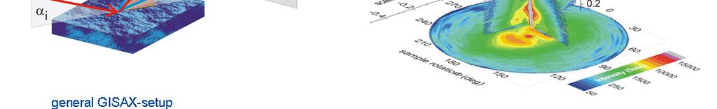
13 Surface X-ray Scattering Techniques 13
 S117")


14 What can the Theory Do? Petrov, JVSTA 21 (2003) S117 Microscopic model and calculation of the required energy levels of substrate Growth simulation allows to develop microscopic model of growth Prediction and guidance in growth parameters and surface manipulation Be aware: The cathode is only ~20nmthick! 14
15 M 3 Sb (M: K, Na, Cs)- Cathodes Good knowledge of what is known: Influence of gas pressure on growth Il Island growth film growth transition at 12nm thickness Vertical phase segregation yield to band banding Under layer shifts cathode to red PMT cathodes are with high probability amorphous Band structure calculations of different compounds First PMT like cathode made at Burle with Burle equipment Clear plan how to come from a PMT cathode (amorphous) to a transfer cathode PMT like cathodes will be used for first analytical tests (especially interlayer) 4 x4 design for evaporator compatible with Burle equipment with removable cathode Integration of Burle concept into transfer cathode fabrication fbi i center The center will allow to take out samples which can be transferred to characterization centers (under UHV) 15

16 Short Glance on the Idea (more by Zikri) Heating Chamber 350C over night Surface Cleaning Interlayer Sb layer (~15min at RT) Alkali treatment (~45min at ~160C) Seal at 50 80C SbPton Pt/Mowire Glass inset with pump and gasmanifold Cs, K, Na sources Glass inset with pump and gasmanifold One master plate will allow to process cathode and take 1cm diameter test samples 16
17 The Growth and Characterization Tools used for M 3 Sb (M: K, Na, Cs)- Cathodes Growth: Burle equipment (available in about 3month) Exactrecipe test Engineering issues of evaporators Transfer test Growth & Characterization Chamber (5 6 month) Modifications of recipe Cleaning procedure (ion/atomic source) Base pressure influence on growth and functionality Evaporation versus sputter Sequential versus co evaporation Study of inter layer influence Morphology Electronic properties Indirect structural properties Production facility (9 12 month) Homogeneity test Recipe test 17
18 The Growth and Characterization Tools used for M 3 Sb (M: K, Na, Cs)- Cathodes Characterization: In situ characterization of growth and characterization chamber Optical spectroscopy (UV VIS) VIS) with cryo capability capability (200nm 1600nm) Transmission and reflection Angle dependence Electrical characterization QE Photo conductivity Temperature dependent I V curves Lateral and transversal conductivity Ex situ (non vacuum) characterization AFM UV VIS Structural probes Gracing incidence X ray techniques (in collaboration with John Smedley (BNL) and APS) First beamtime in December Depth and lateral analysis by Igor (more by himself) 18
19 GaN Will be presented by Jim Buckley 19
20 GaAs: The Main Challenges Wavelength optimization Doping profile optimization Minimizing dark current Transfer and bonding technology 20

 Direct bandgap in IR (typical application) Typical absorption length")


21 Wavelength Optimization of Layer Thickness: The Optimization Criteria nm 248nm 873 nm Efficiency i depends d on Probability to absorb photon Probability to reach surface (Probability to escape from surface is thickness independent) Case GaAs (only an example) Direct bandgap in IR (typical application) Typical absorption length for IR: 1µm Absorption length for 400nm: 30nm 100nm Consequences: Cathode has to be by a factor 10 thinner! Photoelectron has defined kinetic energy Thickness is thinner than mean free pathlength Crystallographic direction matters Defect density, strain,. at the interface between cathode and window matters! LAPPD: Second Collaboration Meeting /5/

 Better: creating internal electric field")
22 What Happens in a 100nm Thick GaAs Cathode (400nm Photon) Answer: NO? Creation of hot electron Momentum in cathode plane! (electron will not reach surface if not scattered) Result: Low QE Very slow Solution: Increasing scattering probability (can be done: tuning band structure to phonon distribution) Better: creating internal electric field gradient By doping gradient (what we have done) Or by external electric Field. LAPPD: Second Collaboration Meeting /5/
23 The Doping Profile: The First Steps Doping profile Electric field distribution can be calculated by commercial simulation programs Typical potential difference eV Influence on timing behavior Theoretical potential possible which allows transient time independent from absorption position! Optimization possible even for very hard x rays? LAPPD: Second Collaboration Meeting /5/
24 Is the Doping Profile Stable During Processing Uncalibrate ed Concentration Model Equation Reduced Chi-Sqr ExpDec1 y = A1*exp(-x/t1) + y E-6 Adj. R-Square B Value Standard Error y E-4 A t Zn / 75 As Exponential Fit Depth (nm) Approach: Minimizing process temperature Using simulations to predict doping profile after processing Calibrating simulations with selected samples using SIMS (Igor & Slade) Status: First simulations done by Zeke Insepov In the process of creating SIMS measurements LAPPD: Second Collaboration Meeting /5/


 80")


25 The Emission Layer: The Standard Cleaning and Activation of GaAs As rich Ga rich ee J. J. Surf. Sci. Nanotech. Vol. 5 (2007) LAPPD: Second Collaboration Meeting /5/
 LAPPD: Second Collaboration Meeting 2010 Exact details of surface and Cs")

26 The Activation and Dark Current e J. Surf. Sci. Nanotech. Vol. 5 (2007) Phys. Rev. Lett. 81, (1998) LAPPD: Second Collaboration Meeting 2010 Exact details of surface and Cs contribution tib ti determines dt electronic states of activation layer Dark counts are highly effected by these details Effects of morphology unknown Long term stability depends on exact composition 10/5/


27 Where We are Now? e J Surf. e J. Surf Sci. Sci Nanotech. Nanotech Vol. Vol 5 (2007) LAPPD: Second Collaboration Meeting /5/
28 The Transfer and Bonding Technology 1. Grow thin layer of sacrificial AlGaAs 2. Growth of photocathode, with layers inverted 3. Deposition of intermediate bonding layers (i.e. SiO 2, S ix N x ) Glass substrate First test structured are made and characterized (roughness and shape errors (10x10mm 2 ) 4. Wafer bonded to a glass substrate predeposited bonding layers 5. Bulk of substrate is etched/cmp hd/ away 6. Sacrificial layer removed 7. Photocathode ready for activation 28
29 Bonding Apparatus Schematic Adjustable Height Metal Bracket 3x Guides IR Lamp Graphite Disk Glass window 3x Screw Shielding/ Mirror Glass Block 29
30 Conclusion & Take-Home-Message The selected cathode systems are: M 3 Sb (M: K, Na, Cs) Cathodes GaAs (in collaboration with UIUC) GaN (in collaboration and under lead of WashU) All cathodes of interest follow the same physics principle Similar band structure results in similar thickness requirements Design principles can be transferred between Materials science aspects are different for the three groups Optical, electrical and many structural properties are known: clear program what has to be done ANL is focused: Creating proto type production facility with most cost efficient recipe Creating the foundations that we will be able to cover the full spectral range after 2 years Providing microscopic i and macroscopic characterization i tools Providing state of the art theory support utilizing collaborations Communication with other institutions: First test using the interlayer study 30
Photocathode Status and Plans. JunqiXie, Klaus Attenkofer, ZikriYusof, SeonWu Lee, Alexander Paramonov, Richard Northrop
 Photocathode Status and Plans JunqiXie, Klaus Attenkofer, ZikriYusof, SeonWu Lee, Alexander Paramonov, Richard Northrop The Photocathode Building Blocks at ANL Photo Cathode Infrastructure Addressing 50%
Status of Multi-alkali Photo-cathode Production and Characterization at ANL Junqi Xie, Marcel Demarteau, Sasha Paramonov, Bob Wagner, Zikri Yusof
 Status of Multi-alkali Photo-cathode Production and Characterization at ANL Junqi Xie, Marcel Demarteau, Sasha Paramonov, Bob Wagner, Zikri Yusof LAPPD Collaboration High Energy Physics Division Argonne
Transmission Mode Photocathodes Covering the Spectral Range
 Transmission Mode Photocathodes Covering the Spectral Range 6/19/2002 New Developments in Photodetection 3 rd Beaune Conference June 17-21, 2002 Arlynn Smith, Keith Passmore, Roger Sillmon, Rudy Benz ITT
Erdong Wang Brookhaven National Laboratory
 Characterization of Multi-Alkali antimonide Cathodes at Cryogenic Temperature and their Performance in SRF Gun Erdong Wang Brookhaven National Laboratory 9/9/2015 1 Outline Motivation Multi-alkali photocathode
Factors Affecting QE and Dark Current in Alkali Cathodes. John Smedley Brookhaven National Laboratory
 Factors Affecting QE and Dark Current in Alkali Cathodes John Smedley Brookhaven National Laboratory Outline Desirable Photocathode Properties Low light detection Accelerator cathodes Factors Affecting
CHAPTER 4. SYNTHESIS OF ALUMINIUM SELENIDE (Al 2 Se 3 ) NANO PARTICLES, DEPOSITION AND CHARACTERIZATION
 NANO PARTICLES, DEPOSITION AND CHARACTERIZATION") 40 CHAPTER 4 SYNTHESIS OF ALUMINIUM SELENIDE (Al 2 Se 3 ) NANO PARTICLES, DEPOSITION AND CHARACTERIZATION 4.1 INTRODUCTION Aluminium selenide is the chemical compound Al 2 Se 3 and has been used as a precursor
40 CHAPTER 4 SYNTHESIS OF ALUMINIUM SELENIDE (Al 2 Se 3 ) NANO PARTICLES, DEPOSITION AND CHARACTERIZATION 4.1 INTRODUCTION Aluminium selenide is the chemical compound Al 2 Se 3 and has been used as a precursor
Passivation of InAs and GaSb with novel high dielectrics
 Passivation of InAs and GaSb with novel high dielectrics Professor Minghwei HONG Department of Materials Science and Engineering, National Tsing Hua University 101, Section 2, Kuang-Fu Rd., Hsinchu, Taiwan,
An advantage of thin-film silicon solar cells is that they can be deposited on glass substrates and flexible substrates.
 ET3034TUx - 5.2.1 - Thin film silicon PV technology 1 Last week we have discussed the dominant PV technology in the current market, the PV technology based on c-si wafers. Now we will discuss a different
Amorphous Materials Exam II 180 min Exam
 MIT3_071F14_ExamISolutio Name: Amorphous Materials Exam II 180 min Exam Problem 1 (30 Points) Problem 2 (24 Points) Problem 3 (28 Points) Problem 4 (28 Points) Total (110 Points) 1 Problem 1 Please briefly
Characterisation of Zinc Tin Oxide Thin Films Prepared
 Chapter 4 Characterisation of Zinc Tin Oxide Thin Films Prepared by Co-sputtering 4.1 Introduction This chapter describes the preparation of amorphous zinc tin oxide thin films by co-sputtering technique
Silver Diffusion Bonding and Layer Transfer of Lithium Niobate to Silicon
 Chapter 5 Silver Diffusion Bonding and Layer Transfer of Lithium Niobate to Silicon 5.1 Introduction In this chapter, we discuss a method of metallic bonding between two deposited silver layers. A diffusion
Ivan Bazarov Physics Department, Cornell University. Fundamental processes in III-V photocathodes; application for high-brightness photoinjectors
 Ivan Bazarov Physics Department, Cornell University Fundamental processes in III-V photocathodes; application for high-brightness photoinjectors 07/21/09 I.V. Bazarov, III-V Photocathodes, ERL09 2 Contents
Quo Vadis? The Multi-Alkali Program
 Quo Vadis? The Multi-Alkali Program Klaus A(enkofer PC- Group Goals and Activities Goals of the project High Quantum Efficiency Unclear what number but larger 50% Response opimized at 400nm First approach:
PHYSICSOF SOLARCELLS. Jenny Nelson. Imperial College, UK. Imperial College Press ICP
 im- PHYSICSOF SOLARCELLS Jenny Nelson Imperial College, UK ICP Imperial College Press Contents Preface v Chapter 1 Introduction 1 1.1. Photons In, Electrons Out: The Photovoltaic Effect 1 1.2. Brief History
Spectral selectivity of doped zinc and aluminium oxide thin films prepared by spray pyrolysis for solar energy applications
 Spectral selectivity of doped zinc and aluminium oxide thin films prepared by spray pyrolysis for solar energy applications P C Simpemba 1,2, K Chinyama 1, J Simfukwe 1 and N R Mlyuka 3 1 The Copperbelt
Microstructural Characterization of Materials
 Microstructural Characterization of Materials 2nd Edition DAVID BRANDON AND WAYNE D. KAPLAN Technion, Israel Institute of Technology, Israel John Wiley & Sons, Ltd Contents Preface to the Second Edition
Characterization and erosion of metal-containing carbon layers
 Characterization and erosion of metal-containing carbon layers Martin Balden Max-Planck-Institut für Plasmaphysik, EURATOM Association, D-85748 Garching, Germany Materials Research Division (MF) Outline
Supporting Information. Solution-Processed 2D PbS Nanoplates with Residual Cu 2 S. Exhibiting Low Resistivity and High Infrared Responsivity
 Supporting Information Solution-Processed 2D PbS Nanoplates with Residual Cu 2 S Exhibiting Low Resistivity and High Infrared Responsivity Wen-Ya Wu, Sabyasachi Chakrabortty, Asim Guchhait, Gloria Yan
Interface quality and thermal stability of laser-deposited metal MgO multilayers
 Interface quality and thermal stability of laser-deposited metal MgO multilayers Christian Fuhse, Hans-Ulrich Krebs, Satish Vitta, and Göran A. Johansson Metal MgO multilayers metal of Fe, Ni 80 Nb 20,
Properties of Inverse Opal Photonic Crystals Grown By Atomic Layer Deposition
 Properties of Inverse Opal Photonic Crystals Grown By Atomic Layer Deposition J.S. King 1, C. W. Neff 1, W. Park 2, D. Morton 3, E. Forsythe 3, S. Blomquist 3, and C. J. Summers 1 (1) School of Materials
Thickness and composition analysis of thin film samples using FP method by XRF analysis
 Technical articles Thickness and composition analysis of thin film samples using FP method by XRF analysis Hikari Takahara* 1. Introduction X-ray fluorescence spectroscopy (XRF) is an elemental quantification
Structural and Optical Properties of MnO 2 : Pb Nanocrystalline Thin Films Deposited By Chemical Spray Pyrolysis
 IOSR Journal of Engineering (IOSRJEN) e-issn: 2250-3021, p-issn: 2278-8719 Vol. 3, Issue 4 (April. 2013), V4 PP 52-57 Structural and Optical Properties of MnO 2 : Pb Nanocrystalline Thin Films Deposited
Materials Characterization
 Materials Characterization C. R. Abernathy, B. Gila, K. Jones Cathodoluminescence (CL) system FEI Nova NanoSEM (FEG source) with: EDAX Apollo silicon drift detector (TE cooled) Gatan MonoCL3+ FEI SEM arrived
General Introduction to Microstructure Technology p. 1 What is Microstructure Technology? p. 1 From Microstructure Technology to Microsystems
 General Introduction to Microstructure Technology p. 1 What is Microstructure Technology? p. 1 From Microstructure Technology to Microsystems Technology p. 9 The Parallels to Microelectronics p. 15 The
Time-resolved diffraction profiles and structural dynamics of Ni film under short laser pulse irradiation
 IOP Publishing Journal of Physics: Conference Series 59 (2007) 11 15 doi:10.1088/1742-6596/59/1/003 Eighth International Conference on Laser Ablation Time-resolved diffraction profiles and structural dynamics
Bialkali Photocathode Development
 Bialkali Photocathode Development Ossy Siegmund, Experimental Astrophysics Group, Space Sciences Laboratory, U. California at Berkeley Some LAPD Photocathode Milestones Systematic characterization of Photo-electron
Optically Assisted Metal-Induced Crystallization of Thin Si Films for Low-Cost Solar Cells
 Optically Assisted Metal-Induced Crystallization of Thin Si Films for Low-Cost Solar Cells Wei Chen, Bhushan Sopori, Kim Jones, and Robert Reedy, National Renewable Energy Laboratory, Golden, CO; N. M.
Optical parameter determination of ZrO 2 thin films prepared by sol gel dip coating
 International Journal of ChemTech Research CODEN (USA): IJCRGG ISSN : 0974-490 Vol.6, No.13, pp 534-5346, November 014 MESCon 014 [4th -5 th September 014] National Conference on Material for Energy Storage
Final Report for AOARD Grant FA Development of direct band gap group-iv. March, 2012
 Final Report for AOARD Grant FA2386-11-1-4037 Development of direct band gap group-iv semiconductor with the incorporation of Sn March, 2012 Name of Principal Investigators: Prof. H. H. Cheng - e-mail
Electron Probe Micro-Analysis (EPMA)
") Electron Probe Micro-Analysis (EPMA) Nilanjan Chatterjee, Ph.D. Principal Research Scientist 1 Electron Microprobe Facility Department of Earth, Atmospheric and Planetary Sciences Massachusetts Institute
Electron Probe Micro-Analysis (EPMA) Nilanjan Chatterjee, Ph.D. Principal Research Scientist 1 Electron Microprobe Facility Department of Earth, Atmospheric and Planetary Sciences Massachusetts Institute
Schottky Tunnel Contacts for Efficient Coupling of Photovoltaics and Catalysts
 Schottky Tunnel Contacts for Efficient Coupling of Photovoltaics and Catalysts Christopher E. D. Chidsey Department of Chemistry Stanford University Collaborators: Paul C. McIntyre, Y.W. Chen, J.D. Prange,
Fundamentals of X-ray diffraction and scattering
 Fundamentals of X-ray diffraction and scattering Don Savage dsavage@wisc.edu 1231 Engineering Research Building (608) 263-0831 X-ray diffraction and X-ray scattering Involves the elastic scattering of
Characterization of Nanoscale Electrolytes for Solid Oxide Fuel Cell Membranes
 Characterization of Nanoscale Electrolytes for Solid Oxide Fuel Cell Membranes Cynthia N. Ginestra 1 Michael Shandalov 1 Ann F. Marshall 1 Changhyun Ko 2 Shriram Ramanathan 2 Paul C. McIntyre 1 1 Department
PbS NANO THIN FILM PHOTOCONDUCTIVE DETECTOR
 International Journal of Physics and Research (IJPR) ISSN 2250-0030 Vol. 3, Issue 3, Aug 2013, 21-26 TJPRC Pvt. Ltd. PbS NANO THIN FILM PHOTOCONDUCTIVE DETECTOR SUDAD S. AHMED, EMAN K. HASSAN & FATN EMAD
Properties of Inclined Silicon Carbide Thin Films Deposited by Vacuum Thermal Evaporation
 182 Properties of Inclined Silicon Carbide Thin Films Deposited by Vacuum Thermal Evaporation Oday A. Hamadi, Khaled Z. Yahia, and Oday N. S. Jassim Abstract In this work, thermal evaporation system was
Department of Chemistry, University of California, Davis, California 95616, USA 2
 Enhance Solar Water Splitting Performance by Utilizing Near Infrared Radiation with Composite Films of Hematite and Rare Earth Doped Upconversion Materials Ming Zhang, 1 Yongjing Lin, 2 Thomas J. Mullen,
Supplementary Information
 Supplementary Information Supplementary Figure 1 Characterization of precursor coated on salt template. (a) SEM image of Mo precursor coated on NaCl. Scale bar, 50 μm. (b) EDS of Mo precursor coated on
X-ray Photoelectron Spectroscopy
 X-ray Photoelectron Spectroscopy X-ray photoelectron spectroscopy (XPS) is a non-destructive technique used to analyze the elemental compositions, chemical and electronic states of materials. XPS has a
High Resolution XPS Study of a Thin Cr 2 O Film Grown on Cr 110
 High Resolution XPS Study of a Thin Cr 2 O 3 111 Film Grown on Cr 110 M. Hassel and I. Hemmerich Lehrstuhl F. Physikal. Chemie I, Ruhr-Universität Bochum, Universitätsstr. 150, Bochum 44780, Germany H.
Growth Of TiO 2 Films By RF Magnetron Sputtering Studies On The Structural And Optical Properties
 Journal of Multidisciplinary Engineering Science and Technology (JMEST) Growth Of TiO 2 Films By RF Magnetron Sputtering Studies On The Structural And Optical Properties Ahmed K. Abbas 1, Mohammed K. Khalaf
ZnO thin film deposition on sapphire substrates by chemical vapor deposition
 ZnO thin film deposition on sapphire substrates by chemical vapor deposition Zhuo Chen 1, T. Salagaj 2, C. Jensen 2, K. Strobl 2, Mim Nakarmi 1, and Kai Shum 1, a 1 Physics Department, Brooklyn College
Simultaneous Reflection and Transmission Measurements of Scandium Oxide Thin Films in the Extreme Ultraviolet
 Simultaneous Reflection and Transmission Measurements of Scandium Oxide Thin Films in the Extreme Ultraviolet Introduction Guillermo Acosta, Dr. David Allred, Dr, Steven Turley Brigham Young University
Synthesis and Characterization of DC Magnetron Sputtered ZnO Thin Films Under High Working Pressures
 Accepted Manuscript Synthesis and Characterization of DC Magnetron Sputtered ZnO Thin Films Under High Working Pressures M. Hezam, N. Tabet, A. Mekki PII: S0040-6090(10)00417-7 DOI: doi: 10.1016/j.tsf.2010.03.091
Supporting Information. Quantum Wells
 Supporting Information Real-Time Observation of Exciton-Phonon Coupling Dynamics in Self-Assembled Hybrid Perovskite Quantum Wells Limeng Ni, Uyen Huynh, Alexandre Cheminal, Tudor H. Thomas, Ravichandran
1. Introduction. What is implantation? Advantages
 Ion implantation Contents 1. Introduction 2. Ion range 3. implantation profiles 4. ion channeling 5. ion implantation-induced damage 6. annealing behavior of the damage 7. process consideration 8. comparison
Multilayer Silver / Dielectric Thin-Film Coated Hollow Waveguides for Sensor and Laser Power Delivery Applications
 Multilayer Silver / Dielectric Thin-Film Coated Hollow Waveguides for Sensor and Laser Power Delivery Applications Theory, Design, and Fabrication Carlos M. Bledt a, James A. Harrington a, and Jason M.
Supplementary Figure S1 Crystal structure of the conducting filaments in sputtered SiO 2
 Supplementary Figure S1 Crystal structure of the conducting filaments in sputtered SiO 2 based devices. (a) TEM image of the conducting filament in a SiO 2 based memory device used for SAED analysis. (b)
CHAPTER 4: Oxidation. Chapter 4 1. Oxidation of silicon is an important process in VLSI. The typical roles of SiO 2 are:
 Chapter 4 1 CHAPTER 4: Oxidation Oxidation of silicon is an important process in VLSI. The typical roles of SiO 2 are: 1. mask against implant or diffusion of dopant into silicon 2. surface passivation
Specimen Preparation Technique for a Microstructure Analysis Using the Focused Ion Beam Process
 Specimen Preparation Technique for a Microstructure Analysis Using the Focused Ion Beam Process by Kozue Yabusaki * and Hirokazu Sasaki * In recent years the FIB technique has been widely used for specimen
Hall coefficient, mobility and carrier concentration as a function of composition and thickness of Zn-Te thin films
 Available online at www.pelagiaresearchlibrary.com Advances in Applied Science Research, 2015, 6(4):215-220 ISSN: 0976-8610 CODEN (USA): AASRFC Hall coefficient, mobility and carrier concentration as a
Development of the Large-Area Picosecond Photo-Detectors
 Development of the Large-Area Picosecond Photo-Detectors Andrey Elagin University of Chicago 3 rd Berkeley Workshop on the Direct Detection of Dark Matter LBL, December 6, 2016 Outline LAPPD Overview Commercialization
CHAPTER 3. Experimental Results of Magnesium oxide (MgO) Thin Films
 Thin Films") CHAPTER 3 Experimental Results of Magnesium oxide (MgO) Thin Films Chapter: III ---------------------------------------------------------------- Experimental Results of Magnesium oxide (MgO) Thin Films
CHAPTER 3 Experimental Results of Magnesium oxide (MgO) Thin Films Chapter: III ---------------------------------------------------------------- Experimental Results of Magnesium oxide (MgO) Thin Films
Ruthenium Oxide Films Prepared by Reactive Biased Target Sputtering
 Ruthenium Oxide Films Prepared by Reactive Biased Target Sputtering Hengda Zhang Anthony Githinji 1. Background RuO2 in both crystalline and amorphous forms is of crucial importance for theoretical as
"OPTICAL AND ELECTRICAL PROPERTIES OF ZnTe AND ZnTe:O THIN FILMS DEPOSITED BY CSVT TECHNIQUE"
 "OPTICAL AND ELECTRICAL PROPERTIES OF ZnTe AND ZnTe:O THIN FILMS DEPOSITED BY CSVT TECHNIQUE" M. A. González Trujillo 1, M.L. Albor Aguilera 2 D.A. Rodríguez Morán 3 M. Galván Arellano 4, A. Morales Acevedo
Influence of Annealing Temperature on the Properties of ITO Films Prepared by Electron Beam Evaporation and Ion-Assisted Deposition
 Kasetsart J. (Nat. Sci.) 42 : 362-366 (2008) Influence of Annealing Temperature on the Properties of ITO Films Prepared by Electron Beam Evaporation and Ion-Assisted Deposition Artorn Pokaipisit 1 *, Mati
Polycrystalline and microcrystalline silicon
 6 Polycrystalline and microcrystalline silicon In this chapter, the material properties of hot-wire deposited microcrystalline silicon are presented. Compared to polycrystalline silicon, microcrystalline
P. N. LEBEDEV PHYSICAL INSTITUTE OF THE RUSSIAN ACADEMY OF SCIENCES PREPRINT
 P. N. LEBEDEV PHYSICAL INSTITUTE OF THE RUSSIAN ACADEMY OF SCIENCES PREPRINT 18 CHANNELING A.V. BAGULYA, O.D. DALKAROV, M.A. NEGODAEV, A.S. RUSETSKII, A.P. CHUBENKO, V.G. RALCHENKO, A.P. BOLSHAKOV EFFECT
Band-gap Engineering in Sputter Deposited Amorphous/Microcrystalline Sc x Ga 1-x N
 NASA/CR-2001-211241 ICASE Report No. 2001-36 Band-gap Engineering in Sputter Deposited Amorphous/Microcrystalline Sc x Ga 1-x N Mark E. Little ICASE, Hampton, Virginia Martin E. Kordesch Ohio University,
INFLUENCE OF TiO2 THIN FILM ANNEALING TEMPERATURE ON ELECTRICAL PROPERTIES SYNTHESIZED BY CVD TECHNIQUE
 INFLUENCE OF TiO2 THIN FILM ANNEALING TEMPERATURE ON ELECTRICAL PROPERTIES SYNTHESIZED BY CVD TECHNIQUE F. N. Mohamed, M. S. A. Rahim, N. Nayan, M. K. Ahmad, M. Z. Sahdan and J. Lias Faculty of Electrical
Dielectric II-VI and IV-VI Metal Chalcogenide Thin Films in Hollow Glass Waveguides (HGWs) for Infrared Spectroscopy and Laser Delivery
 for Infrared Spectroscopy and Laser Delivery") Dielectric II-VI and IV-VI Metal Chalcogenide Thin Films in Hollow Glass Waveguides (HGWs) for Infrared Spectroscopy and Laser Delivery Carlos M. Bledt * a, Daniel V. Kopp a, and James A. Harrington a
Dielectric II-VI and IV-VI Metal Chalcogenide Thin Films in Hollow Glass Waveguides (HGWs) for Infrared Spectroscopy and Laser Delivery Carlos M. Bledt * a, Daniel V. Kopp a, and James A. Harrington a
Pre-treatment of low temperature GaN buffer layer deposited on AlN Si substrate by hydride vapor phase epitaxy
 Ž. Surface and Coatings Technology 131 000 465 469 Pre-treatment of low temperature GaN buffer layer deposited on AlN Si substrate by hydride vapor phase epitaxy Ha Jin Kim, Ho-Sun Paek, Ji-Beom Yoo Department
Passivation of SiO 2 /Si Interfaces Using High-Pressure-H 2 O-Vapor Heating
 Jpn. J. Appl. Phys. Vol. 39 (2000) pp. 2492 2496 Part, No. 5A, May 2000 c 2000 The Japan Society of Applied Physics Passivation of O 2 / Interfaces Using High-Pressure-H 2 O-Vapor Heating Keiji SAKAMOTO
Synthesis and Characterization of Zinc Iron Sulphide (ZnFeS) Of Varying Zinc Ion Concentration
 Of Varying Zinc Ion Concentration") International Journal of Science and Technology Volume 5 No. 5, May, 2016 Synthesis and Characterization of Zinc Iron Sulphide (ZnFeS) Of Varying Zinc Ion Concentration I. B. Obasi 1 and J. C. Osuwa 2
International Journal of Science and Technology Volume 5 No. 5, May, 2016 Synthesis and Characterization of Zinc Iron Sulphide (ZnFeS) Of Varying Zinc Ion Concentration I. B. Obasi 1 and J. C. Osuwa 2
Electron field emission properties of tetrahedral amorphous carbon films
 JOURNAL OF APPLIED PHYSICS VOLUME 85, NUMBER 9 1 MAY 1999 Electron field emission properties of tetrahedral amorphous carbon films L. K. Cheah, a) X. Shi, E. Liu, and B. K. Tay Ion Beam Processing Lab,
Damage Threats and Response of Final Optics for Laser-Fusion Power Plants
 Damage Threats and Response of Final Optics for Laser-Fusion Power Plants M. S. Tillack 1, S. A. Payne 2, N. M. Ghoniem 3, M. R. Zaghloul 1 and J. F. Latkowski 2 1 UC San Diego, La Jolla, CA 92093-0417
More on oxidation. Oxidation systems Measuring oxide thickness Substrate orientation Thin oxides Oxide quality Si/SiO2 interface Hafnium oxide
 More on oxidation Oxidation systems Measuring oxide thickness Substrate orientation Thin oxides Oxide quality Si/SiO2 interface Hafnium oxide EE 432/532 oxide measurements, etc 1 Oxidation systems silicon
Supporting Information
 Supporting Information Large-Area, Transfer-Free, Oxide-Assisted Synthesis of Hexagonal Boron Nitride Films and Their Heterostructures with MoS2 and WS2 Sanjay Behura, Phong Nguyen, Songwei Che, Rousan
CEMS study on diluted magneto titanium oxide films prepared by pulsed laser deposition
 Hyperfine Interact (2006) 168:1065 1071 DOI 10.1007/s10751-006-9406-2 CEMS study on diluted magneto titanium oxide films prepared by pulsed laser deposition K. Nomura & K. Inaba & S. Iio & T. Hitosugi
State of the art quality of a GeOx interfacial passivation layer formed on Ge(001)
") APPLICATION NOTE State of the art quality of a Ox interfacial passivation layer formed on (001) Summary A number of research efforts have been made to realize Metal-Oxide-Semiconductor Field Effect Transistors
APPLICATION NOTE State of the art quality of a Ox interfacial passivation layer formed on (001) Summary A number of research efforts have been made to realize Metal-Oxide-Semiconductor Field Effect Transistors
Effect Thickness and Temperature Annealing on Structural and Optical Proportion of CuInTe 2 Thin Film
 AASCIT Journal of Materials 2016; 2(1): 1-5 Published online February 24 2016 (http://www.aascit.org/journal/materials) Effect Thickness and Temperature Annealing on Structural and Optical Proportion of
Supplementary Figure 1 TEM of external salt byproducts. TEM image of some salt byproducts precipitated out separately from the Si network, with
 Supplementary Figure 1 TEM of external salt byproducts. TEM image of some salt byproducts precipitated out separately from the Si network, with non-uniform particle size distribution. The scale bar is
Supplementary Information
 Supplementary Information Facile growth of hierarchical hematite ( -Fe 2 O 3 ) nanopetals on FTO by pulse reverse electrodeposition for photoelectrochemical water splitting Pravin S. Shinde, Geun Ho Go
7 µc-si:h n-i-p solar cells on textured Ag ZnO:Al back reflectors
 7 µc-si:h n-i-p solar cells on textured Ag ZnO:Al back reflectors 7.1 Introduction The present study on ZnO:Al and textured Ag back reflectors is aimed at application in thin film µc-si n-i-p solar cells.
Thin film solar cells
 Thin film solar cells pn junction: a:si cells heterojunction cells: CIGS-based CdTe-based 1 Amorphous Si large concentration of defects N T >10 16 cm -3 ( dangling bonds D +, D -, D o ) passivation of
Section 4: Thermal Oxidation. Jaeger Chapter 3. EE143 - Ali Javey
 Section 4: Thermal Oxidation Jaeger Chapter 3 Properties of O Thermal O is amorphous. Weight Density =.0 gm/cm 3 Molecular Density =.3E molecules/cm 3 O Crystalline O [Quartz] =.65 gm/cm 3 (1) Excellent
SUPPLEMENTARY INFORMATIONS
 SUPPLEMENTARY INFORMATIONS Dynamic Evolution of Conducting Nanofilament in Resistive Switching Memories Jui-Yuan Chen, Cheng-Lun Hsin,,, Chun-Wei Huang, Chung-Hua Chiu, Yu-Ting Huang, Su-Jien Lin, Wen-Wei
Supplimentary Information. Large-Scale Synthesis and Functionalization of Hexagonal Boron Nitride. Nanosheets
 Electronic Supplementary Material (ESI) for Nanoscale. This journal is The Royal Society of Chemistry 2014 Supplimentary Information Large-Scale Synthesis and Functionalization of Hexagonal Boron Nitride
Molecular Beam Epitaxy of Cu(In,Ga)S 2 on Si
S 2 on Si") Workshop 23 Molecular Beam Epitaxy of (In,Ga) 2 on Th. Hahn J. Cieslak H. Metzner J. Eberhardt M. Müller U. Kaiser U. Reislöhner W. Witthuhn J. Kräußlich Universität Jena hahn@pinet.uni-jena.de R. Goldhahn
Workshop 23 Molecular Beam Epitaxy of (In,Ga) 2 on Th. Hahn J. Cieslak H. Metzner J. Eberhardt M. Müller U. Kaiser U. Reislöhner W. Witthuhn J. Kräußlich Universität Jena hahn@pinet.uni-jena.de R. Goldhahn
Heterostructures of Oxides and Semiconductors - Growth and Structural Studies
 Heterostructures of Oxides and Semiconductors - Growth and Structural Studies Beamline 17B1 W20 X-ray Scattering beamline Authors M. Hong and J. R. Kwo National Tsing Hua University, Hsinchu, Taiwan H.
Excimer Laser Annealing of Hydrogen Modulation Doped a-si Film
 Materials Transactions, Vol. 48, No. 5 (27) pp. 975 to 979 #27 The Japan Institute of Metals Excimer Laser Annealing of Hydrogen Modulation Doped a-si Film Akira Heya 1, Naoto Matsuo 1, Tadashi Serikawa
SUPPLEMENTARY INFORMATION
 High Electrochemical Activity of the Oxide Phase in Model Ceria- and Ceria-Ni Composite Anodes William C. Chueh 1,, Yong Hao, WooChul Jung, Sossina M. Haile Materials Science, California Institute of Technology,
Czochralski Crystal Growth
 Czochralski Crystal Growth Crystal Pulling Crystal Ingots Shaping and Polishing 300 mm wafer 1 2 Advantage of larger diameter wafers Wafer area larger Chip area larger 3 4 Large-Diameter Wafer Handling
Bulk crystal growth. A reduction in Lg will increase g m and f oper but with some costs
 Bulk crystal growth The progress of solid state device technology has depended not only on the development of device concepts but also on the improvement of materials. A reduction in Lg will increase g
Supporting Online Material for
 www.sciencemag.org/cgi/content/full/327/5961/60/dc1 Supporting Online Material for Polarization-Induced Hole Doping in Wide Band-Gap Uniaxial Semiconductor Heterostructures John Simon, Vladimir Protasenko,
Molecular Beam Epitaxy Growth of GaAs 1-x Bi x
 Molecular Beam Epitaxy Growth of GaAs 1-x Bi x Dan Beaton, Ryan Lewis, Xianfeng Lu, Mostafa Masnadi-Shirazi, Sebastien Tixier, Erin Young, Martin Adamcyk, UBC, Vancouver, BC B. Fluegel, A. Mascarenhas,
2Dlayer Product Catalog
 2Dlayer Product Catalog Your idea, Our materials! We provide solutions, not just materials. Tel.: 1-919-228-9662 Email: info@2dlayer.com URL: http://2dlayer.com We accept purchase orders and all kinds
Supporting Online Material for
 www.sciencemag.org/cgi/content/full/science.1200448/dc1 Supporting Online Material for Increasing Solar Absorption for Photocatalysis with Black Hydrogenated Titanium Dioxide Nanocrystals This PDF file
In operandi observation of dynamic annealing: a case. Supplementary Material
 In operandi observation of dynamic annealing: a case study of boron in germanium nanowire devices Supplementary Material Maria M. Koleśnik-Gray, 1,3,4 Christian Sorger, 1 Subhajit Biswas, 2,3 Justin D.
High Density Iron Silicide Nanodots Formed by Ultrathin SiO 2 Film Technique
 Available online at www.sciencedirect.com Procedia Engineering 36 (2012 ) 382 387 IUMRS-ICA 2011 High Density Iron Silicide Nanodots Formed by Ultrathin SiO 2 Film Technique Yoshiaki Nakamura a,b* a Graduate
EUV optics lifetime Radiation damage, contamination, and oxidation
 EUV optics lifetime Radiation damage, contamination, and oxidation M. van Kampen ASML Research 10-11-2016 Preamble Slide 2 ASML builds lithography scanners High-resolution photocopiers Copies mask pattern
AMORPHOUS SILICON DIOXIDE LAYER FOR HIGH EFFICIENCY CRYSTALLINE SOLAR CELLS
 International Journal of Nanotechnology and Application (IJNA) ISSN(P): 2277-4777; ISSN(E): 2278-9391 Vol. 6, Issue 5, Dec 2016, 1-6 TJPRC Pvt. Ltd. AMORPHOUS SILICON DIOXIDE LAYER FOR HIGH EFFICIENCY
Study of The Structural and Optical Properties of Titanium dioxide Thin Films Prepared by RF Magnetron sputtering
 Study of The Structural and Optical Properties of Titanium dioxide Thin Films Prepared by RF Magnetron sputtering Aqeel K. Hadi 1, Muneer H.Jaduaa 1, Abdul- Hussain K. Elttayef 2 1 Wasit University - College
AIMCAL Fall Technical Conference & 19th International Conference on Vacuum Web Coating
 AIMCAL Fall Technical Conference & 19th International Conference on Vacuum Web Coating A.G. Talma, R. Schlatmann, J.W.G. Mahy Akzo Nobel Chemicals bv, P.O. Box 9300, 6800 SB Arnhem, The Netherlands. Phone
Lecture contents. Heteroepitaxy Growth technologies Strain Misfit dislocations. NNSE 618 Lecture #24
 1 Lecture contents Heteroepitaxy Growth technologies Strain Misfit dislocations Epitaxy Heteroepitaxy 2 Single crystalline layer on Single crystalline substrate Strong layer-substrate interaction orientation
Ceramic Processing Research
 Journal of Ceramic Processing Research. Vol. 9, No. 6, pp. 638~642 (2008) J O U R N A L O F Ceramic Processing Research Study of Ga-Doped ZnO films deposited on PET substrates by DC magnetron sputtering
Nucleation and growth of nanostructures and films. Seongshik (Sean) Oh
 Oh") Nucleation and growth of nanostructures and films Seongshik (Sean) Oh Outline Introduction and Overview 1. Thermodynamics and Kinetics of thin film growth 2. Defects in films 3. Amorphous, Polycrystalline
Nucleation and growth of nanostructures and films Seongshik (Sean) Oh Outline Introduction and Overview 1. Thermodynamics and Kinetics of thin film growth 2. Defects in films 3. Amorphous, Polycrystalline
Thermoelectric properties of Bi 2 Te 3 and Sb 2 Te 3 and its bilayer thin films
 Indian Journal of Pure & Applied Physics Vol. 48, February 2010, pp. 115-120 Thermoelectric properties of Bi 2 Te 3 and Sb 2 Te 3 and its bilayer thin films P P Pradyumnan* & Swathikrishnan Department
Red luminescence from Si quantum dots embedded in SiO x films grown with controlled stoichiometry
 Red luminescence from Si quantum dots embedded in films grown with controlled stoichiometry Zhitao Kang, Brannon Arnold, Christopher Summers, Brent Wagner Georgia Institute of Technology, Atlanta, GA 30332
Electronic Supplementary Information
 Electronic Supplementary Material (ESI) for ChemComm. This journal is The Royal Society of Chemistry 2016 Electronic Supplementary Information Thermally Induced Recrystallization of MAPbI 3 Perovskite
Deposited by Sputtering of Sn and SnO 2
 Journal of the Korean Ceramic Society Vol. 49, No. 5, pp. 448~453, 2012. http://dx.doi.org/10.4191/kcers.2012.49.5.448 Comparative Study of Nitrogen Incorporated SnO 2 Deposited by Sputtering of Sn and