Nanofabrication Prof. Stephen Y. Chou NanoStructure Laboratory
|
|
|
- Peregrine Smith
- 6 years ago
- Views:
Transcription
1 Nanofabrication Prof. Stephen Y. Chou Department of Electrical Engineering Princeton University 1
2 Acknowledgment Dr. Paul Fischer Dr. Yun Wang Dr. Jay Guo Dr. Peter Klauss Dr. Jim Wang Dr. Longtin He Dr. Linhshu Kong Dr. Wei Zhang Dr. Larry Zhuang Dr. Gary Li Dr. Wei Wu Dr. Rich Yu Dr. Jian Gu Dr. Paru Deshpende Dr. Allan Chang Harry Gao All other NSL members Students in my ELE547 class Some work was performed at the University of Minnesota Supported in part by DARPA, ONR and ARO 2
3 Outline Top-Down Approaches -- Conventional lithography (radiation-based) -- Nanoimprint and nanoprint (non-radiation-based) -- Etching Bottom-Up Approaches -- Self assembly -- Guided self-assembly -- Molecular epitaxy Commercial Nanoimprint tools and solutions 3
4 Nanotechnology Leads to Discovery and Innovation Because.. As a device size becomes less than a fundamental physical length scale, conventional theory may no longer apply. -- S.Y. Chou (Nanotech Report 1998) 4
5 Examples of Fundamental Length Scales and Impaccts Optical Phonon Scattering Length _ >Velocity overshoot and Fast transistors Phase Coherent Length _ >Quantum effects Nanocrystal size _ >single crystal on α-substrate New way to build transistors Quantum energy > RT energy _ >Room Temp Single Electron Devices 1 μm 100 nm 10 nm 1 nm Visible light wavelength _ >Subwavelength optics Optical ICs Magnetic domain wall size _ >New fast magnetic devices Ultra-high density memories DNA Persistent Length _ >DNA sorter Molecule size _ >Molecular electronics 5
6 Nanotechnology Impacts Multi-Disciplines Nanotechnology makes old products new ways and new products that can t be made before. It will grow exponentially to multi-dimensional, multi-billion dollar market in a few years. Semicon. ICs Displays Data Storage MEMS Optical Comm Nanotechnology Artificial Materials Biotech Pharm Chemical Synthesis etc 6
7 Nanofabrication Nanofabrication is the vehicle to bring us to the nanotechnology dreamland of multi-dimensional and multi-trillion-dollars markets. Today, we do not yet have a commercial general-purpose nanomanufacturing tool. Without nanofabrication, nanotechnology will be a pie in the sky. (--S.Y. Chou) 7
8 Nanofabrications Top-Down Approaches -- Conventional lithography (radiation-based) -- Nanoimprint and nanoprint (non-radiation-based) -- Etching Bottom-Up Approaches -- Self assembly -- Guided self-assembly -- Molecular epitaxy 8
9 Different Lithographies Radiation-based lithography Photolithography (deep ultraviolet, x-ray, extreme ultraviolet) Electron beam lithography (scanning, projection) Ion beam lithography (scanning, projection) Maskless lithographies Non-radiation-based lithography Nanonimprint Nanoprinting (ink stamping, ink jet, dip-pen lithography) 9

10 Photolithography A. Mask Making B. Exposures Whitesides, Sci. American,
11 Physics of Radiation Based Lithography Theoretical resolution = (K 1 λ) / (NA) Theoretical Depth of Focus = (K 2 λ) / (NA) 2 (λ: wavelength, NA: numerical aperture, K 1 and K 2 are constants) Real resolution also depends on resist properties, mask resolution enhancement technologies, etch process Stulen, at al., IEEE J. of Quan, Elec.,
12 12
13 13
14 14
15 15

16 16


17 Examples of EUV Lithography Stulen, at al., IEEE J. of Quan, Elec., nm elbow patterns Chapman, et al., J. Vac. Sci. Tech. B,

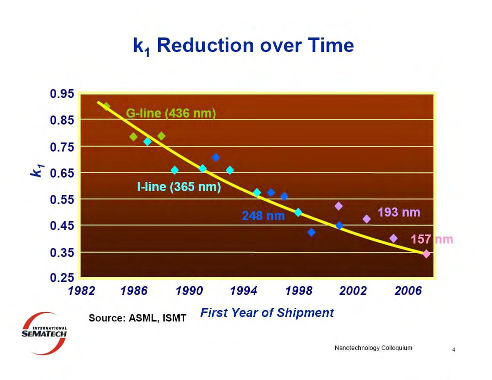
18 Conventional Lithography Can Not Offer the Resolution, Cost, and Exposure Area Needed for Nanomanufacturing NGL??..? Tool Price PEL, etc $50M 90 nm $20M $10M Manufacturing 2006 Limited to: nm? -- 1 sq-in area -- $40M/tool 18
19 Nanoimprint Lithography (NIL) a Solution to Nano-manufacturing mold resist substrate 10nm 1. Imprint Press Mold Remove Mold 2. Pattern Transfer RIE Chou, US Pat 5,772,905, 6,309,580, APL, Vol. 67, 3114 (1995); Science, Vol. 272, 85 (1996) 19
 10 nm")
20 10 nm Diameter, 40nm Period Imprint Mold (After 12 Imprints) 10 nm NanoStructureLaboratory 20
21 10 nm Diameter, 40 nm Period and 60 nm Deep Holes Imprinted into PMMA 10 nm 21

22 10 nm Diameter & 40 nm Period Ti/Au Dot Array by NIL and Lift-Off 10 nm 22


23 6 nm Diameter & 65 nm Period Ti/Au Dot Array by NIL and Lift-Off 23

24 6 nm Half-Pitch Resist Lines by NIL NIL resist (cured) Quartz Monomer (1.4 nm) 6 nm Half-Pitch 8.5 nm Half-Pitch 17 nm Half-Pitch 6 nm = 9 monomers 6 nm Polymerization within a constrained geometry Austin and Chou, J of Nanotechnology


25 Vertical Sidewall of 70 nm Resist Lines by Photo Curable/Transfer Nanoimprinting UV Curable Resist Transfer Layer Resist 25

26 20 nm Half-Pitch & 0.04 µm 2 SRAM Contact Layer by NIL 20 nm CD control measurements: Mean: 21.5 nm σ (sigma): 1.3 nm ITRS roadmap spec: 2016! Austin and Chou, J of Nanotech, Aug Nanonex NX-2000 NIL machines Nanonex NXR-2010 resist 26
 Princeton 0.")

27 Comparison of SRAM Metal Layers by 65 nm Node Photolithography & Nanoimprint lithography Intel 1.13 µm 2 cell by 193 nm lithography & phase masks (2002) Princeton 0.04 µm 2 cell by nanoimprint lithography 110 nm Half-Pitch 20 nm Half-Pitch Reduction: -- 6X in linear -- 30X in area ftp://download.intel.com/research/sili con/borodovskyphotomaskjapan040 2pres.pdf Austin and Chou, J Nanotech Nanonex NX-2000 NanoStructure NIL machines Laboratory Nanonex NXR-2010 resist 27
Nanoimprint Lithography and Applications at Hewlett Packard Labs
 Nanoimprint Lithography and pplications at Hewlett Packard Labs Wei Wu Quantum Science Research dvanced Studies HP Labs, Hewlett-Packard Email: wei.wu@hp.com Outline Background Motivation Nanoimprint lithography
Introduction to Micro/Nano Fabrication Techniques. Date: 2015/05/22 Dr. Yi-Chung Tung. Fabrication of Nanomaterials
 Introduction to Micro/Nano Fabrication Techniques Date: 2015/05/22 Dr. Yi-Chung Tung Fabrication of Nanomaterials Top-Down Approach Begin with bulk materials that are reduced into nanoscale materials Ex:
Nanoimprinting in Polymers and Applications in Cell Studies. Albert F. YEE Chemical Engineering & Materials Science UC Irvine
 Nanoimprinting in Polymers and Applications in Cell Studies Albert F. YEE Chemical Engineering & Materials Science UC Irvine Presentation outline Motivation Reversal imprinting Soft inkpad imprinting on
Introduction to Lithography
 Introduction to Lithography G. D. Hutcheson, et al., Scientific American, 290, 76 (2004). Moore s Law Intel Co-Founder Gordon E. Moore Cramming More Components Onto Integrated Circuits Author: Gordon E.
Integration of Block-Copolymer with Nano- Imprint Lithography: Pushing the Boundaries of Emerging Nano-Patterning Technology
 Integration of Block-Copolymer with Nano- Imprint Lithography: Pushing the Boundaries of Emerging Nano-Patterning Technology April 2010 update SNL Geoff Brennecka (PI) Bruce Burckel Matt George Jack Skinner
3. Overview of Microfabrication Techniques
 3. Overview of Microfabrication Techniques The Si revolution First Transistor Bell Labs (1947) Si integrated circuits Texas Instruments (~1960) Modern ICs More? Check out: http://www.pbs.org/transistor/background1/events/miraclemo.html
SCIENCE CHINA Technological Sciences. Replication of large area nanoimprint stamp with small critical dimension loss
 SCIENCE CHINA Technological Sciences RESEARCH PAPER March 2012 Vol.55 No.3: 600 605 doi: 10.1007/s11431-011-4695-3 Replication of large area nanoimprint stamp with small critical dimension loss MENG FanTao
Thermal Nanoimprinting Basics
 Thermal Nanoimprinting Basics Nanoimprinting is a way to replicate nanoscale features on one surface into another, like stamping copies are made by traditional fabrication techniques (optical/ebeam lith)
Imprint Lithography: Getting to the Next Level
 Imprint Lithography: Getting to the Next Level May 26 SEMECH Litho Forum James E. Ellenson; ; Ken Kramer; im S. Hostetler; Laura King; William M. ong Hewlett-Packard Company 24 Hewlett-Packard Development
One-kilobit cross-bar molecular memory circuits at 30-nm half-pitch fabricated by nanoimprint lithography
 Appl. Phys. A 80, 1173 1178 (2005) DOI: 10.1007/s00339-004-3176-y Applied Physics A Materials Science & Processing w. wu 1, g.-y. jung 1 d.l. olynick 2 j. straznicky 1 z. li 1 x. li 1 d.a.a. ohlberg 1
EECS130 Integrated Circuit Devices
 EECS130 Integrated Circuit Devices Professor Ali Javey 9/13/2007 Fabrication Technology Lecture 1 Silicon Device Fabrication Technology Over 10 15 transistors (or 100,000 for every person in the world)
Figure 6. Rare-gas atom-beam diffraction patterns. These results were obtained by Wieland Schöllkopf and Peter Toennies at the Max-Planck Institute
 Figure 6. Rare-gas atom-beam diffraction patterns. These results were obtained by Wieland Schöllkopf and Peter Toennies at the Max-Planck Institute in Göttingen, Germany, using a freestanding, 100nm-period
Micro- and Nano-Technology... for Optics
 Micro- and Nano-Technology...... for Optics 3.2 Lithography U.D. Zeitner Fraunhofer Institut für Angewandte Optik und Feinmechanik Jena Electron Beam Column electron gun beam on/of control magnetic deflection
Applications of Nano Patterning Process 1. Patterned Media
 Applications of Nano Patterning Process 1. Patterned Media Contents Introduction Part. 1. Nanoimprinting on Glass Substrate for Patterned Media Part. 2. Nanoinjection Molding of Nanopillars for Patterned
In-Situ Monitoring of Pattern Filling in Nano-Imprint Lithography Using Surface Plasmon Resonance
 Copyright 2011 American Scientific Publishers All rights reserved Printed in the United States of America Journal of Nanoscience and Nanotechnology Vol. 11, 1 6, 2011 In-Situ Monitoring of Pattern Filling
Surface Acoustic Wave fabrication using nanoimprint. Zachary J. Davis, Senior Consultant,
 Surface Acoustic Wave fabrication using nanoimprint Zachary J. Davis, Senior Consultant, zjd@teknologisk.dk Center for Microtechnology & Surface Analysis Micro and Nano Technology Sensor Technology Top
Polymer-based Microfabrication
 Polymer-based Microfabrication PDMS SU-8 PMMA Hydrogel 1 Soft Lithography Developed by Whitesides, et. al A set of techniques for microfabrication based on the use of lithography, soft substrate materials
More on VLSI Fabrication Technologies. Emanuele Baravelli
 More on VLSI Fabrication Technologies Emanuele Baravelli Some more details on: 1. VLSI meaning 2. p-si epitaxial layer 3. Lithography 4. Metallization 5. Process timings What does VLSI mean, by the way?
ELEC 3908, Physical Electronics, Lecture 4. Basic Integrated Circuit Processing
 ELEC 3908, Physical Electronics, Lecture 4 Basic Integrated Circuit Processing Lecture Outline Details of the physical structure of devices will be very important in developing models for electrical behavior
Micro & nanofabrica,on
 Micro & nanofabrica,on Photolitography : - contact - projec,on Electron Beam lithography (EBL) Nano imprint lithography Etching Contact Photolithography Substrate (e.g. Silicon wafer) Photoresist spinning
Chapter 7 NANOIMPRINTED CIRCULAR GRATING DISTRIBUTED FEEDBACK DYE LASER
 Chapter 7 66 NANOIMPRINTED CIRCULAR GRATING DISTRIBUTED FEEDBACK DYE LASER 7.1 Introduction In recent years, polymer dye lasers have attracted much attention due to their low-cost processing, wide choice
Introduction to Micro and Nanotechnologies
 Micro & Nanobioengineering Lab Biomedical Engineering Department McGill University Introduction to Micro and Nanotechnologies David Juncker david.juncker@mcgill.ca www.bmed.mcgill.ca/nanomed McGill, Nov
Innovative Roll-to-Roll Equipment & Material Development Suite
 Innovative Roll-to-Roll Equipment & Material Development Suite For Next Generation Technology from Carpe Diem Technologies and the University of Massachusetts Amherst By John Berg, Dimitur Benchev, James
From microelectronics down to nanotechnology.
 From microelectronics down to nanotechnology sami.franssila@tkk.fi Contents Lithography: scaling x- and y-dimensions MOS transistor physics Scaling oxide thickness (z-dimension) CNT transistors Conducting
Dr. Priyabrat Dash Office: BM-406, Mob: Webpage: MB: 205
 Email: dashp@nitrkl.ac.in Office: BM-406, Mob: 8895121141 Webpage: http://homepage.usask.ca/~prd822/ MB: 205 Nonmanufacturing In continuation from last class... 2 Top-Down methods Mechanical-energy methods
Invited paper. Issues on nanoimprint lithography with a single-layer resist structure. Applied Physics A Materials Science & Processing
 Appl. Phys. A 81, 1331 1335 (2005) DOI: 10.1007/s00339-005-3313-2 g.y. jung 1 w. wu 1 s. ganapathiappan 1 d.a.a. ohlberg 1 m. saif islam 2 x. li 1 d.l. olynick 3 h. lee 4 y. chen 5 s.y. wang 1 w.m. tong
Development of Imprint Materials for the Step and Flash Imprint Lithography Process
 Development of Imprint Materials for the Step and Flash Imprint Lithography Process Frank Xu a, Nick Stacey b, Michael Watts a, Van Truskett a, Ian McMackin a, Jin Choi a, Philip Schumaker a, Ecron Thompson
Technology process. It s very small world. Electronics and Microelectronics AE4B34EM. Why is the integration so beneficial?
 It s very small world Electronics and Microelectronics AE4B34EM 9. lecture IC processing technology Wafer fabrication Lithography How to get 1 000 000 000 Components to 1 cm 2 Human hair on the surface
Large Area Functional Surfaces By Roll-to-Roll Nanoimprint Lithography Project: APPOLO
 Large Area Functional Surfaces By Roll-to-Roll Nanoimprint Lithography Project: APPOLO Mr. Theodoros Tachtsidis Nanotypos 23rd and 24th of June Amsterdam Core Overview Nanotypos is a pioneering research
Nano-imprinting Lithography Technology І
 Nano-imprinting Lithography Technology І Agenda Limitation of photolithograph - Remind of photolithography technology - What is diffraction - Diffraction limit Concept of nano-imprinting lithography Basic
Contents. From microelectronics down to nanotechnology
 Contents From microelectronics down to nanotechnology sami.franssila@tkk.fi Lithography: scaling x- and y-dimensions MOS transistor physics Scaling oxide thickness (z-dimension) CNT transistors Conducting
Contents. From microelectronics down to nanotechnology. Top down nanotechnology. Writing patterns
 Contents From microelectronics down to nanotechnology sami.franssila@tkk.fi Lithography: scaling x- and y-dimensions MOS transistor physics Scaling oxide thickness (z-dimension) CNT transistors Conducting
Proton beam fabrication of nickel stamps for nanoimprint lithography
 Nuclear Instruments and Methods in Physics Research B 231 (2005) 407 412 www.elsevier.com/locate/nimb Proton beam fabrication of nickel stamps for nanoimprint lithography K. Ansari *, P.G. Shao, J.A. van
ECE280: Nano-Plasmonics and Its Applications. Week5. Extraordinary Optical Transmission (EOT)
") ECE280: Nano-Plasmonics and Its Applications Week5 Extraordinary Optical Transmission (EOT) Introduction Sub-wavelength apertures in metal films provide light confinement beyond the fundamental diffraction
ECE280: Nano-Plasmonics and Its Applications Week5 Extraordinary Optical Transmission (EOT) Introduction Sub-wavelength apertures in metal films provide light confinement beyond the fundamental diffraction
Nano-Scale Manufacturing:
 The Second U.S.-Korea Forum on Nanotechnology: Nanomanufacturing Research and Education Nano-Scale Manufacturing: Top-down, Bottom-up and System Engineering Cheng Sun, Xiang Zhang Center of Scalable and
Center for Scalable and Integrated NanoManufacturing
 Nanomanufacturing Summit 2009 Center for Scalable and Integrated NanoManufacturing Li Zeng Berkeley, CA Boston, MA May 27-29, 2009 UC Berkeley UCLA Stanford MIT UNCC HP Labs NSF Nanoscale Science and Engineering
Electron Beam Lithography - key enabling technology in nanofabrication. Frank Dirne
 Electron Beam Lithography - key enabling technology in nanofabrication Frank Dirne Moore s Law (x2/2 yr) Moore s Law EBL Electron Beam Lithography - key enabling technology in nanofabrication - Principles
Design, Fabrication, Optimization and Verification of FePt based Bit Patterned Media
 Design, Fabrication, Optimization and Verification of FePt based Bit Patterned Media Jian-Ping Wang, Professor MINT Center & Electrical and Computer Engineering Department, Graduate Faculty of Chemical
National Nanotechnology Infrastructure Network Vol.3 # 1. A Periodic Newsletter of NNIN News and Announcements NNIN. New Equipment and Processes
 National Nanotechnology Infrastructure Network Vol.3 # 1 A Periodic Newsletter of NNIN News and Announcements Feb. 2007 NNIN The National Nanotechnology Infrastructure Network consists of 13 nanotechnology
Texas Nanofabrication Facility (TNF)
") National Nanotechnology Coordinated Infrastructure Atlanta Jan 2017 Texas Nanofabrication Facility (TNF) Sanjay K. Banerjee Site Director TNF UT-Austin Capabilities 3 centers from UT: MRC (NNIN), TMI and
National Nanotechnology Coordinated Infrastructure Atlanta Jan 2017 Texas Nanofabrication Facility (TNF) Sanjay K. Banerjee Site Director TNF UT-Austin Capabilities 3 centers from UT: MRC (NNIN), TMI and
A Novel Extrusion Microns Embossing Method of Polymer Film
 Modern Mechanical Engineering, 2012, 2, 35-40 http://dx.doi.org/10.4236/mme.2012.22005 Published Online May 2012 (http://www.scirp.org/journal/mme) A Novel Extrusion Microns Embossing Method of Polymer
Tunable Nanoscale Plasmon Antenna for Localization and Enhancement of Optical Energy. Douglas Howe
 Tunable Nanoscale Plasmon Antenna for Localization and Enhancement of Optical Energy Douglas Howe Applied Optics Spring 2008 Table of Contents Abstract... 3 Introduction... 4 Surface Plasmons... 4 Nano
Fabrication Technology, Part I
 EEL5225: Principles of MEMS Transducers (Fall 2003) Fabrication Technology, Part I Agenda: Oxidation, layer deposition (last lecture) Lithography Pattern Transfer (etching) Impurity Doping Reading: Senturia,
NANO-FABRICATION FOR MESOSCOPIC PHYSICS
 NANO-FABRICATION FOR MESOSCOPIC PHYSICS Frédéric Pierre CNRS, Laboratory of Photonics and Nanostructures (LPN), Marcoussis, France ϕ Nano Team LPN PLAN Overview Electron beam lithography Step by step realization
A Uniform Pressure Apparatus for Micro/Nanoimprint Lithography Equipment
 Paper: A Uniform Pressure Apparatus for Micro/Nanoimprint Lithography Equipment Jian-Shian Lin Λ;ΛΛ, Chieh-Lung Lai Λ, Ya-Chun Tu Λ, Cheng-Hua Wu Λ, and Yoshimi Takeuchi ΛΛ Λ Mechanical and System Research
Simple UV-based Soft-lithography Process for. Fabrication of Low-Loss Polymer PSQ-L-based. Waveguides
 Simple UV-based Soft-lithography Process for Fabrication of Low-Loss Polymer PSQ-L-based Waveguides Jie Teng 1, 2, 4, Stijn Scheerlinck 4, Geert Morthier 4, Roel Baets 4, Hongbo Zhang 2,3, Xigao Jian 2,3,
WP7 JRA2 JRA2 Research on High Precision Manufacturing. Investigation of optimum NIL stamp fabrication method to copy sub-10 nm BCP features
 DELIVERABLE REPORT WP7 JRA2 JRA2 Research on High Precision Manufacturing D7.1 Investigation of optimum NIL stamp fabrication method to copy sub-10 nm BCP features M18 NFFA-Europe has received funding
Creating Greater Capacity on Smaller Spaces
 Creating Greater Capacity on Smaller Spaces Manufacturability of Pattern Media Babak Heidari, Obducat, Sweden Obducat Overview Company Background Founded in 1989 Facilities in Sweden (HQ) and in Cambridge
Title: Localized surface plasmon resonance of metal nanodot and nanowire arrays studied by far-field and near-field optical microscopy
 Contract Number: AOARD-06-4074 Principal Investigator: Heh-Nan Lin Address: Department of Materials Science and Engineering, National Tsing Hua University, 101, Sec. 2, Kuang Fu Rd., Hsinchu 30013, Taiwan
Step and Flash Imprint Lithography for sub-100nm Patterning
 Step and Flash Imprint Lithography for sub-100nm Patterning Matthew Colburn, Annette Grot, Marie Amistoso, Byung Jin Choi, Todd Bailey, John Ekerdt, S.V. Sreenivasan, James Hollenhorst, C. Grant Willson
Vertically aligned Ni magnetic nanowires fabricated by diblock-copolymer-directed Al thin film anodization
 Vertically aligned Ni magnetic nanowires fabricated by diblock-copolymer-directed Al thin film anodization Researcher: Kunbae (Kevin) Noh, Graduate Student, MAE Dept. and CMRR Collaborators: Leon Chen,
MODERN COMPUTER TENDING TOWARDS NANOTECHNOLOGY MAKING GRATE GROWTH IN 21 ST CENTURY
 MODERN COMPUTER TENDING TOWARDS NANOTECHNOLOGY MAKING GRATE GROWTH IN 21 ST CENTURY Mrs. Jayashree Yadannavar Department of Information Technology,MIT AOE, Alandi(D),Pune ABSTRACT At present in the field
Advanced Polymers And Resists For Nanoimprint Lithography
 Q U A L I T Y A S S U R A N C E MICROSYSTEMS & NANOSYSTEMS SPECIAL REPORT Advanced Polymers And Resists For Nanoimprint Lithography Numerous polymer systems specifically designed for nanoimprint lithography
Sub-5 nm Structures Process Development and Fabrication Over Large Areas
 A S Jugessur,, 2017, 1:1 SciFed Nanotech Research Letters Research Article Open Access Sub-5 nm Structures Process Development and Fabrication Over Large Areas * A S Jugessur * University of Iowa Microfabrication
Chapter 3 Silicon Device Fabrication Technology
 Chapter 3 Silicon Device Fabrication Technology Over 10 15 transistors (or 100,000 for every person in the world) are manufactured every year. VLSI (Very Large Scale Integration) ULSI (Ultra Large Scale
NIL defect performance toward High volume mass production
 NIL defect performance toward High volume mass production Masayuki Hatano a, Kei Kobayashi a, Hiroyuki Kashiwagi a, Hiroshi Tokue a, Takuya Kono a, Nakasugi Tetsuro a, Eun Hyuk Choi b, Wooyung Jung b a
ADVANCED NANOSCALE SCIENCE & ENGINEERING NANOPHYSICS SEMESTER MONTH CONTENT LAB THEMES SKILLS ASSESSMENTS. Cutting it Down to Nano Lab
 September Nano-Intro (Same topics for nanophysics and nanochem) Topic I: GOT NANO? Unit 1 Nano -Calculations Metric Review 2 Dimensional Analysis 3 Dimensional Analysis Sci. Not. & Sig. Figs. NanoDefinitions
Development of the equipments for nano photonic crystal
 Development of the equipments for nano photonic crystal Wen-Yuh Jywe, Jing-Chung Shen, Chien-Hung Liu, Shang-Liang Chen, Tung Hsien Hsieh, Li-Li Duan, Chen-Hua She Department of Automation Engineering
EUV optics lifetime Radiation damage, contamination, and oxidation
 EUV optics lifetime Radiation damage, contamination, and oxidation M. van Kampen ASML Research 10-11-2016 Preamble Slide 2 ASML builds lithography scanners High-resolution photocopiers Copies mask pattern
Multiphoton lithography based 3D micro/nano printing Dr Qin Hu
 Multiphoton lithography based 3D micro/nano printing Dr Qin Hu EPSRC Centre for Innovative Manufacturing in Additive Manufacturing University of Nottingham Multiphoton lithography Also known as direct
Soft Lithography. Jin-Goo Park. Materials and Chemical Engineering Hanyang University, Ansan. Electronic Materials and Processing Lab.
 Hanyang University Soft Lithography Jin-Goo Park Materials and Chemical Engineering Hanyang University, Ansan Electronic Materials and Processing Lab. Introduction to Soft Lithography Research Micro- Electro-
Nano-imprint Technology on LED Applications
 Nano-imprint Technology on LED Applications Dr. Sean Lin September 4, 2013 Outline Background Introduction Industry Updates on Nanoimprint Technology (NIT) Photonic Crystal (PhC) LEDs by NIT Other Work
Nanoscale Imaging, Material Removal and Deposition for Fabrication of Cutting-edge Semiconductor Devices
 Hitachi Review Vol. 65 (2016), No. 7 233 Featured Articles Nanoscale Imaging, Material Removal and Deposition for Fabrication of Cutting-edge Semiconductor Devices Ion-beam-based Photomask Defect Repair
Lessons Learned from SEMATECH s Nanoimprint Program
 Accelerating the next technology revolution Lessons Learned from SEMATECH s Nanoimprint Program Matt Malloy Lloyd C. Litt Mac Mellish 10/19/11 Copyright 2010 SEMATECH, Inc. SEMATECH, and the SEMATECH logo
Applications of LIGA on Micro-punching Process for Metallic Materials
 Materials Science Forum Vols. 505-507 (2006) pp. 55-60 online at http://www.scientific.net (2006) Trans Tech Publications, Switzerland Applications of LIGA on Micro-punching Process for Metallic Materials
Lithography options for the 32nm half pitch node. imec
 Lithography options for the 32nm half pitch node imec 2006 1 Lithography options for the 32nm half pitch node Luc Van den hove and Kurt Ronse ITRS roadmap:32 nm half pitch requirement Product Half-Pitch,
(12) Patent Application Publication (10) Pub. No.: US 2013/ A1
 Patent Application Publication (10) Pub. No.: US 2013/ A1") (19) United States US 2013 0220971 A1 (12) Patent Application Publication (10) Pub. No.: US 2013/0220971 A1 Bijkerk et al. (43) Pub. Date: (54) METHOD FOR MANUFACTURING A (30) Foreign Application Priority
(19) United States US 2013 0220971 A1 (12) Patent Application Publication (10) Pub. No.: US 2013/0220971 A1 Bijkerk et al. (43) Pub. Date: (54) METHOD FOR MANUFACTURING A (30) Foreign Application Priority
2010 NMS RESEARCH NEEDS IN PATTERNING, NANOENGINEERED MATERIALS, AND METROLOGY July 8, 2010
 Introduction Patterning and nanoengineered materials are recognized today as critical to the success of high volume device manufacturing, with enhanced functional density. It also is understood that unless
Lithography Independent Fabrication of Nano-MOS-Transistors with W = 25 nm and L = 25 nm
 Lithography Independent Fabrication of Nano-MOS-Transistors with W = 25 nm and L = 25 nm J. T. Horstmann John_Horstmann@ieee.org C. Horst Christian.Horst@udo.edu K. F. Goser goser@ieee.org Abstract The
Fabrication characteristics of a line-and-space pattern and a dot pattern on a roll mold by using electron-beam lithography
 0123456789 Bulletin of the JSME Journal of Advanced Mechanical Design, Systems, and Manufacturing Vol.10, No.5, 2016 Fabrication characteristics of a line-and-space pattern and a dot pattern on a roll
Supplementary information for
 Supplementary information for Metal hierarchical patterning by direct nanoimprint lithography Boya Radha 1,2, Su Hui Lim 2,3, Mohammad S. M. Saifullah 2* and Giridhar U. Kulkarni 1* 1 Chemistry and Physics
NanoSystemsEngineering: NanoNose Final Status, March 2011
 1 NanoSystemsEngineering: NanoNose Final Status, March 2011 The Nanonose project is based on four research projects (VCSELs, 3D nanolithography, coatings and system integration). Below, the major achievements
AAO MCP Substrate Development at ANL. High Energy Physics Division, Materials Science Division Argonne National Laboratory Friday, June 11, 2010
 AAO MCP Substrate Development at ANL Seon W. Lee and H. Hau Wang High Energy Physics Division, Materials Science Division Argonne National Laboratory Friday, June 11, 2010 Contents What is AAO? Advantage
Fabrication and Layout
 ECEN454 Digital Integrated Circuit Design Fabrication and Layout ECEN 454 3.1 A Glimpse at MOS Device Polysilicon Aluminum ECEN 475 4.2 1 Material Classification Insulators Glass, diamond, silicon oxide
Polymer-based optical interconnects using nano-imprint lithography
 Polymer-based optical interconnects using nano-imprint lithography Arjen Boersma,Sjoukje Wiegersma Bert Jan Offrein, Jeroen Duis, Jos Delis, Markus Ortsiefer, Geert van Steenberge, MikkoKarppinen, Alfons
NANOSCALE MANUFACTURING
 NANOSCALE MANUFACTURING From the Bottom Up: DNA Focus Todd Nilsen Overview Current Techniques Lithography Mechanical Stamping Advantages/Disadvantages New Technology Bottom Up Approach Using DNA Protein
Choi, Jun-Hyuk Korea Institute of Machinery & Materials
 The 11 th US-Korea Nanosymposium Choi, Jun-Hyuk 2014. 09. 29 Korea Institute of Machinery & Materials About KIMM Nano-research Bldg Clean RM Five Research Divisions; 1. Advanced Manufacturing Sys. 2. Extreme
Effect of nanoimprinted surface relief on Si and Ge nucleation and ordering
 Microelectronics Journal 37 (2006) 1481 1485 www.elsevier.com/locate/mejo Effect of nanoimprinted surface relief on Si and Ge nucleation and ordering T.I. Kamins a,, A.A. Yasseri a,1, S. Sharma a,2, R.F.W.
Fabrication Of Metallic Antenna Arrays Using Nanoimprint Lithography
 University of Central Florida Electronic Theses and Dissertations Masters Thesis (Open Access) Fabrication Of Metallic Antenna Arrays Using Nanoimprint Lithography 2013 Yu-Wei Lin University of Central
SUPPLEMENTARY INFORMATION
 Large-area, flexible 3D optical negative index metamaterial formed by nanotransfer printing DebashisChanda 1, KazukiShigeta 1, Sidhartha Gupta 1, Tyler Cain 1, Andrew Carlson 1, Agustin Mihi 1, Alfred
NSF Nanomanufacturing (NM) Program (Food for Thought) Khershed P. Cooper, PhD
 Program (Food for Thought) Khershed P. Cooper, PhD") NSF Nanomanufacturing (NM) Program (Food for Thought) Khershed P. Cooper, PhD Program Director, Nanomanufacturing ENG-CMMI National Science Foundation Arlington, VA 2013 NSF Nanoscale Science and Engineering
NSF Nanomanufacturing (NM) Program (Food for Thought) Khershed P. Cooper, PhD Program Director, Nanomanufacturing ENG-CMMI National Science Foundation Arlington, VA 2013 NSF Nanoscale Science and Engineering
Fabrication of 3-D Microstructures with Sidewall Inclination Controlled by Development Temperature
 Fabrication of 3-D Microstructures with Sidewall Inclination Controlled by Development Temperature Mitsuhiro Horade 1 amd Susumu Sugiyama 2 1) Research Organization of Science and Engineering, Ritsumeikan
DPN 5000 System. Figure 1: The DPN 5000 System. Page 1 of 5. Created on 9/9/2011 Revision
 Introduction NanoInk s is a dedicated, versatile instrument capable of nanopatterning a variety of materials with nanoscale accuracy and precision. With NanoInk s proprietary MEMs devices and deposition
Bistable nano-structured photoalignment surface by nanoimprint lithography
 Bistable nano-structured photoalignment surface by nanoimprint lithography Chung-Yung Lee (SID Member) Man-Chun Tseng (SID Student Member) Jacob Yeuk-Lung Ho (SID Member) Vladimir G. Chigrinov (SID Fellow)
Photolithography. Dong-Il Dan Cho. Seoul National University Nano/Micro Systems & Controls Laboratory
 Lecture 9: Photolithography School of Electrical l Engineering i and Computer Science, Seoul National University Nano/Micro Systems & Controls Laboratory Email: dicho@snu.ac.kr URL: http://nml.snu.ac.kr
Lateral epitaxial growth of two-dimensional layered semiconductor heterojunctions
 Lateral epitaxial growth of two-dimensional layered semiconductor heterojunctions Xidong Duan, Chen Wang, Jonathan Shaw, Rui Cheng, Yu Chen, Honglai Li, Xueping Wu, Ying Tang, Qinling Zhang, Anlian Pan,
STABILITY OF SELF-ASSEMBLED MONOLAYER SURFACTANT COATING IN THERMAL NANOIMPRINT. A Thesis PATRICK GORDON LUNSFORD
 STABILITY OF SELF-ASSEMBLED MONOLAYER SURFACTANT COATING IN THERMAL NANOIMPRINT A Thesis by PATRICK GORDON LUNSFORD Submitted to the Office of Graduate Studies of Texas A&M University in partial fulfillment
Subwavelength gratings fabricated on semiconductor substrates via E-beam lithography and lift-off method
 Optical and Quantum Electronics (2005) 37:425 432 Ó Springer 2005 DOI 10.1007/s11082-005-2027-1 Subwavelength gratings fabricated on semiconductor substrates via E-beam lithography and lift-off method
Superionic Solid State Stamping (S4)
") Superionic Solid State Stamping (S4) Lead Faculty Researcher: Placid Ferreira Department: Materials Science & Engineering Hsu et al, Nano Letters, 2007 1. Description: This dry, single step, electrochemical
Superionic Solid State Stamping (S4) Lead Faculty Researcher: Placid Ferreira Department: Materials Science & Engineering Hsu et al, Nano Letters, 2007 1. Description: This dry, single step, electrochemical
Today s Class. Materials for MEMS
 Lecture 2: VLSI-based Fabrication for MEMS: Fundamentals Prasanna S. Gandhi Assistant Professor, Department of Mechanical Engineering, Indian Institute of Technology, Bombay, Recap: Last Class What is
Advanced resists for e-beam lithography: processing, exposure and characterization (Part II)
") Advanced resists for e-beam lithography: processing, exposure and characterization (Part II) Dra. Mariana Pojar de Melo Prof. Dr. Antonio Carlos Seabra Dep. Eng. de Sistemas Eletrônicos Escola Politécnica
Advanced resists for e-beam lithography: processing, exposure and characterization (Part II) Dra. Mariana Pojar de Melo Prof. Dr. Antonio Carlos Seabra Dep. Eng. de Sistemas Eletrônicos Escola Politécnica
We are IntechOpen, the first native scientific publisher of Open Access books. International authors and editors. Our authors are among the TOP 1%
 We are IntechOpen, the first native scientific publisher of Open Access books 3,350 108,000 1.7 M Open access books available International authors and editors Downloads Our authors are among the 151 Countries
FABRICATION ENGINEERING MICRO- NANOSCALE ATTHE AND. Fourth Edition STEPHEN A. CAMPBELL. of Minnesota. University OXFORD UNIVERSITY PRESS
 AND FABRICATION ENGINEERING ATTHE MICRO- NANOSCALE Fourth Edition STEPHEN A. CAMPBELL University of Minnesota New York Oxford OXFORD UNIVERSITY PRESS CONTENTS Preface xiii prrt i OVERVIEW AND MATERIALS
NIR High-Efficiency Subwavelength DiEractive Structures In Semiconductors.
 c NIR High-Efficiency Subwavelength DiEractive Structures In Semiconductors. R.E. Smith, M.E. Warren, J.R. Wendt and G.A. Vawter Sandia National Laboratories Albuquerque, NM 87185-0603 Abstract: We have
THIN FILM THICKNESS MEASUREMENT FOR EVALUATION OF RESIDUAL LAYER OF NANO-IMPRINT LITHOGRAPHY USING NEAR-FIELD OPTICS
 9 th INTERNATIONAL SYMPOSIUM ON MEASUREMENT AND QUALITY CONTROL (9 th ISMQC) November 21 24, 27, IIT Madras THIN FILM THICKNESS MEASUREMENT FOR EVALUATION OF RESIDUAL LAYER OF NANO-IMPRINT LITHOGRAPHY
Study on microprobe processing by LIGA on Si
 Study on microprobe processing by LIGA on Si Fundamental study for 3-D 3 D mold -Report 1-1 Teppei Kimura, JEM Japan (Japan Electronic Materials Corp.) Tadashi Hattori Himeji Institute of Technology in
Hybrid Nanoimprint-Soft Lithography with Sub-15 nm Resolution
 Hybrid Nanoimprint-Soft Lithography with Sub-15 nm Resolution NANO LETTERS 2009 Vol. 9, No. 6 2306-2310 Zhiwei Li, Yanni Gu, Lei Wang, Haixiong Ge,*, Wei Wu,*, Qiangfei Xia, Changsheng Yuan, Yanfeng Chen,
Introduction to Nanoscience and Nanotechnology
 Introduction to Nanoscience and Nanotechnology ENS 463 2. Principles of Nano-Lithography by Alexander M. Zaitsev alexander.zaitsev@csi.cuny.edu Tel: 718 982 2812 Office 4N101b 1 Lithographic patterning
Electron Beam Induced Processes and their Applicability to Mask Repair
 & Electron Beam Induced Processes and their Applicability to Mask Repair Hans W.P. Koops (1), Volker Boegli (1), Klaus Edinger (1), Johannes Bihr (2), Jens Greiser (2), (1) NaWoTec GmbH Rossdorf Germany
SBDUV-APD Solar-Blind Deep UV APDs
 SBDUV-APD Solar-Blind Deep UV APDs Industry Day Dr. Y. K. Chen DARPA 9/18/2018 Distribution Statement A (Approved for Public Release, Distribution Unlimited) 1 SBDUV-APD Technical Background Distribution