Innovative Roll-to-Roll Equipment & Material Development Suite
|
|
|
- Philomena Charles
- 5 years ago
- Views:
Transcription


1 Innovative Roll-to-Roll Equipment & Material Development Suite For Next Generation Technology from Carpe Diem Technologies and the University of Massachusetts Amherst By John Berg, Dimitur Benchev, James Watkins, Jeff Morse
2 Overview In the Beginning NIL Inkjet and Sintered Conductors Challenges Alignment and Combined Technologies Next Gen and New Facility 2


3 In the Beginning
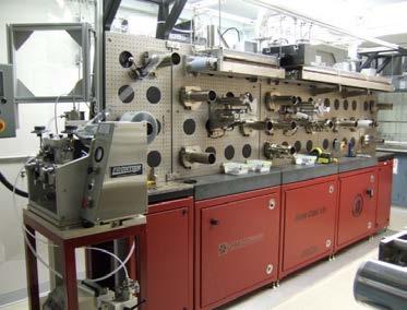
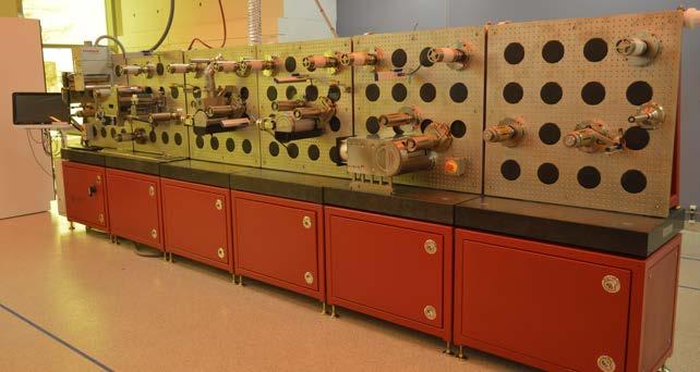
4 UMass / CHM R2R NIL Tool Touch one side of web only Vacuum rolls Vibration isolation loops Tension Control Energy transfer variables secret to success 4

5 R2RNIL 500 nm to Sub-100 nm Gratings John, Tang, Rothstein, Watkins,, Carter Nanotechnology, 2013,
6 Nanoimprint Lithography - Intermediate Assessment NIL Offers Very High Pattern Resolution R2R NIL Offers High Rate Continuous Patterning Current NIL Resists Offer Limited Functionality Can We Imprint Directly into Useful Materials?


7 Large Area Antimicrobial Textured Layers NIL and R2RNIL Challenge: Can we replicate Sharklet pattern? PFPE daughter mold from 6 inch master with K. Carter


8 Direct Imprinting of Patterned Metal Oxides Nanostructures Patterned ITO for transistors Patterned TiO 2 for solar cells Patterned YSZ for SOFC ACS Appl. Mater. Interfaces 2012, 4, Nanoscale, 2012, 4, 4464 Patterned electrodes for nanofluidics ACS Nano, 2011, 5, Patterned dielectrics for photonic devices Adv. Mater. 2010, 22,


9 Direct Imprinting NIL of Patterned Metal Oxides Nanostructures


10 Layer by Layer Printing of Crystalline Metal Oxides Pattern TiO 2 using NIL Planarize using polymers Remove planarizing layer at the end by calcination

11 What About Metals? Nanoimprinted/Photonically Sintered Cu Electrodes/Contacts


12 Conductors?...Inkjet-Printed Silver Pattern / Photonic Sintering Photonic sintering Optimized conditions: 420V, 5000us, 12uP, 6x, 25% duty Resistance ~ 5Ω Prototype Production


13 Cu Printed on PET followed by Photonic Sintering

14 UMass R2R Inkjet / Photonic Sintering Tool

15 Drying Cu Nanoink R2R

16 SIntering Cu R2R

17 Sintered Cu R2R


18 What Else? - Residual-Free Imprinting of Graphene 100 um 10 um 5 um 2 um
19 Nanoimprint for Microfluidic Channels Prototype Production
20 Challenges for Making more Complicated Devices Alignment of Ink jet to Nano Imprint Pattern Optical Lithography to Nano Imprint Ink Jet to Optical Lithography Pattern Optical Lithography to Ink jet Pattern Ink Jet to Ink jet Pattern Distorted Flexible Substrates and Masks Masters Seamless and Long life 20


21 Direct Write Stepper Lithography, Inkjet, & Interferometric Alignment / Metrology Ink jet Fiducial Projected Target Aligned Projected Pattern TI DLP UV projected through Nikon Objective Interferometer Alignment through Nikon Objective 21


22 Contact / Proximity Overlay Alignment for high speed & NIL Alignment Development 3 Cameras with microns/pixel 300 frames per second 5 axes Alignment Motion Control to.1 micron Exposure UV Laser Polygon Scanned Nominal line speed 12 ipm.. Energy limited Assuming ~150 mj/cm 2 22
23 Contact / Proximity Overlay Alignment NIL Alignment Development 23
24 Practical Limits on Contact Alignment, Resolution Mylar Mask Quality 20-40K DPI resolution micron resolution but micron min feature for < $300 (18 x 6 ) 1.25 micron on flexible glass for $5-10K (18 x 6 ) Substrate Distortion Mask-Web Tracking Requires Servo Following Error Match Encoder Resolution 1 million counts/rev is only.5 micron! Not good enough!!! But, Encoders available with 1 billion counts/ revolution.5 nanometer resolution Velocity for servo has not zero error but matched error which is a function of velocity Force and vibration isolation Image System Web, Mask, and Web plus Mask all <.1 micron positioning resolution on required fiducials 24


25 Roller building blocks lead to ALD Vacuum Roller I Vacuum Roller II + Atomic Layer Deposition Drum Air Bearing / Air Turn 25

26 Spatial ALD in Development First runs now 26


27 Institute for Applied Life Sciences UMass Amherst
 R2R Deep Reactive Ion Etching / Ion Beam Milling (CF 4, O 2, SF 6,")

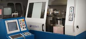
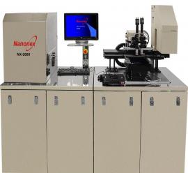
28 APRM: Advanced Print and Roll-to-Roll Manufacturing Demonstration Facility Rolling Opening Dr y Organic La Electronics b Print Cure Sinter Class 10,000 R2R Clean Room Facility Slit/Laminate Characterization / Optics Wet Chemistry R2R Sputter Deposition 4 Target System (Choose - Cu, Au, Pd, ITO, Al 2 O 3, SiO 2, Ni, Ti) R2R Deep Reactive Ion Etching / Ion Beam Milling (CF 4, O 2, SF 6, Ar, CHF 3, He) R2R Spatial ALD Advanced R2R Coater Gravure and Slot Die with Controlled Emissions Exhaust R2R Inkjet Printing (Xaar) with Xenon Pulse Flash Lamp and NIR Cure (NovaCentrix) R2R Alignment Technology with overlay resolution of 1 micron Advanced R2R NIL with through master exposure and solvent assisted NIL R2R Optical Contact Lithography Sheet-Based and R2R Pick and Place Secondary processes: slitting/cutting, layer release/transfer, integration/bonding/assembly Dry Room Optomec Aerosol printing system Sheet-based Inkjet and Optical Cure Nanonex Batch NIL Tool NX-2608BA CHM legacy tools: UV-Assisted Nanoimprint and Nanocoater
29 Current Technology: Coating, Sputter, Etch, Laminate etc 29


30 Future Technology: Nanoimprint and Direct Print of Sub- Micron Inorganic Conductors, Semiconductors, Dielectrics 30

31 Emerging Technology: R2R Ink Jet with Photonic Cure, R2R Pick and Place, Aerosol Jet, Spatial ALD 31

32 THANK YOU 32
Photonic Drying Pulsed Light as a low Temperature Sintering Process
 Photonic Drying Pulsed Light as a low Temperature Sintering Process Lou Panico Xenon Corporation W E S T E R N M I C H I G A N U N I V E R S I T Y PRESENTATION OVERVIEW What is Printed Electronics Materials
Manipulation and control of spatial ALD layers for flexible devices. Aimcal Memphis 2016; Edward Clerkx
 Manipulation and control of spatial ALD layers for flexible devices Meyer Burger Netherlands Equipment manufacturer Functional inkjet printing Based in Eindhoven, the Netherlands Part of world-wide Meyer
Introduction to Micro/Nano Fabrication Techniques. Date: 2015/05/22 Dr. Yi-Chung Tung. Fabrication of Nanomaterials
 Introduction to Micro/Nano Fabrication Techniques Date: 2015/05/22 Dr. Yi-Chung Tung Fabrication of Nanomaterials Top-Down Approach Begin with bulk materials that are reduced into nanoscale materials Ex:
Thermal Nanoimprinting Basics
 Thermal Nanoimprinting Basics Nanoimprinting is a way to replicate nanoscale features on one surface into another, like stamping copies are made by traditional fabrication techniques (optical/ebeam lith)
Technologies challenges and opportunities in UV and thermal Nanoimprint Lithography Roll2Roll technologies for flexible hybrid electronics
 Technologies challenges and opportunities in UV and thermal Nanoimprint Lithography Roll2Roll technologies for flexible hybrid electronics Thomas Kolbusch, Vice President, Coatema GmbH Wilfried Schipper,
Advances in Intense Pulsed Light Solutions For Display Manufacturing. XENON Corporation Dr. Saad Ahmed Japan IDW 2016
 Advances in Intense Pulsed Light Solutions For Display Manufacturing XENON Corporation Dr. Saad Ahmed Japan IDW 2016 Talk Outline Introduction to Pulsed Light Applications in Display UV Curing Applications
Towards scalable fabrication of high efficiency polymer solar cells
 Towards scalable fabrication of high efficiency polymer solar cells Hui Joon Park 2*, Myung-Gyu Kang 1**, Se Hyun Ahn 3, Moon Kyu Kang 1, and L. Jay Guo 1,2,3 1 Department of Electrical Engineering and
Roll-to-Roll Nanoimprint - 6 회 -
 Roll-to-Roll Nanoimprint - 6 회 - 목차 Click to add Title 1 Roll to Roll nanoimprint Introduction : Continuous Production System (Roll-to-Roll) Fabrication Processes Fabrication of nano roll mold 2 Case study
LOW TEMPERATURE PHOTONIC SINTERING FOR PRINTED ELECTRONICS. Dr. Saad Ahmed XENON Corporation November 19, 2015
 LOW TEMPERATURE PHOTONIC SINTERING FOR PRINTED ELECTRONICS Dr. Saad Ahmed XENON Corporation November 19, 2015 Topics Introduction to Pulsed Light Photonic sintering for Printed Electronics R&D Tools for
Laser treatment of gravure-printed ITO films on PET
 Laser treatment of gravure-printed ITO films on PET Howard V Snelling, Anton A Serkov, Jack Eden, Rob J Farley Physics, School of Mathematical and Physical Sciences, University of Hull, HU6 7RX, UK Presentation
Surface Acoustic Wave fabrication using nanoimprint. Zachary J. Davis, Senior Consultant,
 Surface Acoustic Wave fabrication using nanoimprint Zachary J. Davis, Senior Consultant, zjd@teknologisk.dk Center for Microtechnology & Surface Analysis Micro and Nano Technology Sensor Technology Top
THIN METALLIC LAYERS STRUCTURED BY E-BEAM LITHOGRAPHY. Miroslav HORÁČEK, Vladimír KOLAŘÍK, Michal URBÁNEK, František MATĚJKA, Milan MATĚJKA
 THIN METALLIC LAYERS STRUCTURED BY E-BEAM LITHOGRAPHY Miroslav HORÁČEK, Vladimír KOLAŘÍK, Michal URBÁNEK, František MATĚJKA, Milan MATĚJKA Ústav přístrojové techniky AV ČR, v. v. i., Královopolská 147,
Advances in Printing nano Cu and Using Existing Cu Based Manufacturing Processes. Michael J. Carmody Chief Scientist, Intrinsiq Materials
 Advances in Printing nano Cu and Using Existing Cu Based Manufacturing Processes Michael J. Carmody Chief Scientist, Intrinsiq Materials Why Use Copper? Lower Cost than Silver. Print on Numerous Substrates.
Chapter 3 Silicon Device Fabrication Technology
 Chapter 3 Silicon Device Fabrication Technology Over 10 15 transistors (or 100,000 for every person in the world) are manufactured every year. VLSI (Very Large Scale Integration) ULSI (Ultra Large Scale
Dr. Priyabrat Dash Office: BM-406, Mob: Webpage: MB: 205
 Email: dashp@nitrkl.ac.in Office: BM-406, Mob: 8895121141 Webpage: http://homepage.usask.ca/~prd822/ MB: 205 Nonmanufacturing In continuation from last class... 2 Top-Down methods Mechanical-energy methods
PulseForge TM. Curing Copper and other Thin-Film Materials. Stan Farnsworth, VP Marketing
 PulseForge TM Curing Copper and other Thin-Film Materials at Production Speeds Stan Farnsworth, VP Marketing Oct 2009 2009 PulseForge 3100 and Pulsed Thermal Processing www.novacentrix.com 2 NovaCentrix
Introduction to Lithography
 Introduction to Lithography G. D. Hutcheson, et al., Scientific American, 290, 76 (2004). Moore s Law Intel Co-Founder Gordon E. Moore Cramming More Components Onto Integrated Circuits Author: Gordon E.
Nanoimprinting in Polymers and Applications in Cell Studies. Albert F. YEE Chemical Engineering & Materials Science UC Irvine
 Nanoimprinting in Polymers and Applications in Cell Studies Albert F. YEE Chemical Engineering & Materials Science UC Irvine Presentation outline Motivation Reversal imprinting Soft inkpad imprinting on
Fabrication Technology, Part I
 EEL5225: Principles of MEMS Transducers (Fall 2003) Fabrication Technology, Part I Agenda: Oxidation, layer deposition (last lecture) Lithography Pattern Transfer (etching) Impurity Doping Reading: Senturia,
1.3.2 Nanotechnology Nanoporosity Deposition Methods Dissolution Methods
 Table of Contents 1. Metal Finishing 1 1.1 Introduction 1 1.1.1 Description of Industrial Activity Covered 1 1.1.2 Environmental and Legislative Background 3 1.1.3 Emerging Technology or Research? 4 1.2
Fraunhofer ENAS Current results and future approaches in Wafer-level-packaging FRANK ROSCHER
 Fraunhofer ENAS - Current results and future approaches in Wafer-level-packaging FRANK ROSCHER Fraunhofer ENAS Chemnitz System Packaging Page 1 System Packaging Outline: Wafer level packaging for MEMS
Advanced Polymers And Resists For Nanoimprint Lithography
 Q U A L I T Y A S S U R A N C E MICROSYSTEMS & NANOSYSTEMS SPECIAL REPORT Advanced Polymers And Resists For Nanoimprint Lithography Numerous polymer systems specifically designed for nanoimprint lithography
Imprint Lithography: Getting to the Next Level
 Imprint Lithography: Getting to the Next Level May 26 SEMECH Litho Forum James E. Ellenson; ; Ken Kramer; im S. Hostetler; Laura King; William M. ong Hewlett-Packard Company 24 Hewlett-Packard Development
EECS130 Integrated Circuit Devices
 EECS130 Integrated Circuit Devices Professor Ali Javey 9/13/2007 Fabrication Technology Lecture 1 Silicon Device Fabrication Technology Over 10 15 transistors (or 100,000 for every person in the world)
Organic Substrate - LCP
 Organic Substrate - LCP Why consider LCP as a substrate? Liquid Crystal Polymer (LCP) can be used as a high performance multilayer substrate Excellent electrical properties (ε r ~ 3.10 and tanδ=0.002)
LOW TEMPERATURE PHOTONIC SINTERING FOR PRINTED ELECTRONICS. Saad Ahmed, PhD Manager-Engineering
 LOW TEMPERATURE PHOTONIC SINTERING FOR PRINTED ELECTRONICS Saad Ahmed, PhD Manager-Engineering Topics Introduction Significance of nanotechnology Conductive inks Pulsed light for sintering Reel-to-reel
Three-dimensional SU-8 structures by reversal UV imprint
 Three-dimensional SU-8 structures by reversal UV imprint W. Hu, a B. Yang, C. Peng, and S. W. Pang b Solid State Electronics Laboratory, Department of Electrical Engineering and Computer Science, The University
Compact hybrid plasmonic-si waveguide structures utilizing Albanova E-beam lithography system
 Compact hybrid plasmonic-si waveguide structures utilizing Albanova E-beam lithography system Introduction Xu Sun Laboratory of Photonics and Microwave Engineering, Royal Institute of Technology (KTH),
Production and analysis of optical gratings and nanostructures created by laser based methods
 Summary of the Ph.D. thesis Production and analysis of optical gratings and nanostructures created by laser based methods Kiss Bálint Supervisor: Dr. Vass Csaba Research fellow Doctoral School in Physics
VISION INNOVATE INSPIRE DELIVER
 INSPIRE Vision About NovaCentrix Photonic Curing INNOVATE History Applications DELIVER Our Products SimPulse Conductive Inks NanoPowders VISION NovaCentrix partners with you to take ideas from inspiration
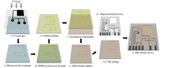
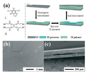
Integration and Scalable Manufacturing of Printed Microfluidic Devices
 Integration and Scalable Manufacturing of Printed Microfluidic Devices Jeffrey Morse, Aditi Naik, Yiliang Zhou, David Gonzalez, Brenda Warren, Uzodinma Okoroanyanwu and James J. Watkins University of Massachusetts,
Photovoltaics & Solar Thermals. Thin-film equipment. Customized. FHR Anlagenbau GmbH I
 Photovoltaics & Solar Thermals Thin-film equipment. Customized. FHR Anlagenbau GmbH I www.fhr.de FHR Anlagenbau GmbH is an innovative enterprise in the branch of vacuum processing and thin-film technologies.
Fabrication characteristics of a line-and-space pattern and a dot pattern on a roll mold by using electron-beam lithography
 0123456789 Bulletin of the JSME Journal of Advanced Mechanical Design, Systems, and Manufacturing Vol.10, No.5, 2016 Fabrication characteristics of a line-and-space pattern and a dot pattern on a roll
Flexible functional devices at mass production level with the FLEx R2R sald platform
 Flexible functional devices at mass production level with the FLEx R2R sald platform D. Spee, W. Boonen, D. Borsa and E. Clerkx Meyer Burger (Netherlands) B.V. Meyer Burger Introduction to sald Challenges
Micro Fabrication : Soft Lithography
 Micro Fabrication : Soft Lithography Last Class: 1. Electrowetting on Dielectric (EWOD) 2. Setup in EWOD 3. Basic Manipulations : Mixing Splitting, Translation 4. Optoelectrowetting (OEW) Today s Contents:
Fabrication Technologies and Instruments. The available fabrication technologies and instruments for fabricating the sub-wavelength
 Chapter 3 Fabrication Technologies and Instruments 3.1 Introduction The available fabrication technologies and instruments for fabricating the sub-wavelength grating will be described in this chapter.
Choi, Jun-Hyuk Korea Institute of Machinery & Materials
 The 11 th US-Korea Nanosymposium Choi, Jun-Hyuk 2014. 09. 29 Korea Institute of Machinery & Materials About KIMM Nano-research Bldg Clean RM Five Research Divisions; 1. Advanced Manufacturing Sys. 2. Extreme
WP7 JRA2 JRA2 Research on High Precision Manufacturing. Investigation of optimum NIL stamp fabrication method to copy sub-10 nm BCP features
 DELIVERABLE REPORT WP7 JRA2 JRA2 Research on High Precision Manufacturing D7.1 Investigation of optimum NIL stamp fabrication method to copy sub-10 nm BCP features M18 NFFA-Europe has received funding
From Vacuum to Atmosphere and back an in-house Process Chain for Different Products
 From Vacuum to Atmosphere and back an in-house Process Chain for Different Products Dr. Steffen Günther Vacuum coating low pressure 10-1 10-4 Pa (10-3 10-6 mbar) unhindered particle movement no unintended
About Cambridge NanoTech Atomic Layer Deposition (ALD) Selected Applications Manufacturing Considerations ALD Reactors Summary
 Selected Applications Manufacturing Considerations ALD Reactors Summary") About Cambridge NanoTech Atomic Layer Deposition (ALD) Selected Applications Manufacturing Considerations ALD Reactors Summary Founded in 2003 by Dr. Jill Becker Located in Cambridge, MA Grew directly
About Cambridge NanoTech Atomic Layer Deposition (ALD) Selected Applications Manufacturing Considerations ALD Reactors Summary Founded in 2003 by Dr. Jill Becker Located in Cambridge, MA Grew directly
Progress in Roll-to-Roll Atomic Layer Deposition
 Progress in Roll-to-Roll Atomic Layer Deposition Council for Chemical Research Barrier Workshop Arlington, Virginia September 20, 2012 E. Dickey Lotus Applied Technology Outline ALD for barrier films ALD
NANO-FABRICATION FOR MESOSCOPIC PHYSICS
 NANO-FABRICATION FOR MESOSCOPIC PHYSICS Frédéric Pierre CNRS, Laboratory of Photonics and Nanostructures (LPN), Marcoussis, France ϕ Nano Team LPN PLAN Overview Electron beam lithography Step by step realization
Photonic Sintering of Silver for Roll-to-Roll Printed Electronics. Saad Ahmed, PhD Manager-Engineering
 Photonic Sintering of Silver for Roll-to-Roll Printed Electronics Saad Ahmed, PhD Manager-Engineering Topics Introduction Significance of nanotechnology Conductive inks Pulsed light for sintering Reel-to-reel
Developments in Printed Electronics
 Developments in Printed Electronics Processing - Photonic Curing Materials - Copper Oxide Reduction Inks Simulation - Numerical Thermal Processing Stan Farnsworth VP Marketing Oct 2011 NovaCentrix in the
Nanofabrication Prof. Stephen Y. Chou NanoStructure Laboratory
 Nanofabrication Prof. Stephen Y. Chou Department of Electrical Engineering Princeton University 1 Acknowledgment Dr. Paul Fischer Dr. Yun Wang Dr. Jay Guo Dr. Peter Klauss Dr. Jim Wang Dr. Longtin He Dr.
Amorphous Oxide Transistor Electrokinetic Reflective Display on Flexible Glass
 Amorphous Oxide Transistor Electrokinetic Reflective Display on Flexible Glass Devin A. Mourey, Randy L. Hoffman, Sean M. Garner *, Arliena Holm, Brad Benson, Gregg Combs, James E. Abbott, Xinghua Li*,
Nano-imprinting Lithography Technology І
 Nano-imprinting Lithography Technology І Agenda Limitation of photolithograph - Remind of photolithography technology - What is diffraction - Diffraction limit Concept of nano-imprinting lithography Basic
Enabling new industries with high volume manufacturing: learnings from R2R processing in wearable and flexible displays
 Enabling new industries with high volume manufacturing: learnings from R2R processing in wearable and flexible displays Tobias Stolley, Technologist Applied Materials WEB Coating GmbH Industiral Technologies
Large-area patterning by roller-based nanoimprint lithography
 JOANNEUM RESEARCH Forschungsgesellschaft Institute MATERIALS, Weiz, Austria Large-area patterning by roller-based nanoimprint lithography Ursula Palfinger, Dieter Nees, Stephan Ruttloff, Markus Leitgeb,
Physical Vapor Deposition (PVD) Zheng Yang
 Zheng Yang") Physical Vapor Deposition (PVD) Zheng Yang ERF 3017, email: yangzhen@uic.edu Page 1 Major Fabrication Steps in MOS Process Flow UV light Mask oxygen Silicon dioxide photoresist exposed photoresist oxide
Physical Vapor Deposition (PVD) Zheng Yang ERF 3017, email: yangzhen@uic.edu Page 1 Major Fabrication Steps in MOS Process Flow UV light Mask oxygen Silicon dioxide photoresist exposed photoresist oxide
FABRICATION ENGINEERING MICRO- NANOSCALE ATTHE AND. Fourth Edition STEPHEN A. CAMPBELL. of Minnesota. University OXFORD UNIVERSITY PRESS
 AND FABRICATION ENGINEERING ATTHE MICRO- NANOSCALE Fourth Edition STEPHEN A. CAMPBELL University of Minnesota New York Oxford OXFORD UNIVERSITY PRESS CONTENTS Preface xiii prrt i OVERVIEW AND MATERIALS
EE40 Lec 22. IC Fabrication Technology. Prof. Nathan Cheung 11/19/2009
 Suggested Reading EE40 Lec 22 IC Fabrication Technology Prof. Nathan Cheung 11/19/2009 300mm Fab Tour http://www-03.ibm.com/technology/manufacturing/technology_tour_300mm_foundry.html Overview of IC Technology
Nanofabrication Technologies for Roll-to-Roll Processing Report from the NIST-NNN Workshop September 27-28, 2011
 Nanofabrication Technologies for Roll-to-Roll Processing Report from the NIST-NNN Workshop September 27-28, 2011 Edited by Jeffrey D. Morse, Ph.D. Nanofabrication Technologies for Roll-to-Roll Processing
ABSTRACT: INTRODUCTION:
 ABSTRACT: Nano-Composite Polymer Optical Coatings Tom Faris Vampire Optical Coatings, Inc. P.O. Box 240 Kirkersville, Ohio 43033 (740)-927-5257 f(740)-927-5032 vampirecoatings@earthlink.net Traditionally
Large Area Functional Surfaces By Roll-to-Roll Nanoimprint Lithography Project: APPOLO
 Large Area Functional Surfaces By Roll-to-Roll Nanoimprint Lithography Project: APPOLO Mr. Theodoros Tachtsidis Nanotypos 23rd and 24th of June Amsterdam Core Overview Nanotypos is a pioneering research
Holographix LLC Overview. High quality custom replicated optics and surface relief patterns in production volumes
 Holographix LLC Overview 2018 High quality custom replicated optics and surface relief patterns in production volumes One location in Marlborough, MA. 15,000 sq. ft. facility with additional space available
3. Overview of Microfabrication Techniques
 3. Overview of Microfabrication Techniques The Si revolution First Transistor Bell Labs (1947) Si integrated circuits Texas Instruments (~1960) Modern ICs More? Check out: http://www.pbs.org/transistor/background1/events/miraclemo.html
TSV Processing and Wafer Stacking. Kathy Cook and Maggie Zoberbier, 3D Business Development
 TSV Processing and Wafer Stacking Kathy Cook and Maggie Zoberbier, 3D Business Development Outline Why 3D Integration? TSV Process Variations Lithography Process Results Stacking Technology Wafer Bonding
Atomic Layer Deposition (ALD)
") Atomic Layer Deposition (ALD) ALD provides Uniform, controlled, conformal deposition of oxide, nitride, and metal thin films on a nanometer scale. ALD is a self limiting thin film deposition technique
Atomic Layer Deposition (ALD) ALD provides Uniform, controlled, conformal deposition of oxide, nitride, and metal thin films on a nanometer scale. ALD is a self limiting thin film deposition technique
CONFERENCE EVALUATION FORM
 2015 AIMCAL Web Coating & Handling / SPE FlexPackCon CONFERENCE EVALUATION FORM To upgrade the quality of the Web Coating & Handling / FlexPackCon Conference, we would appreciate your comments. MONDAY,
Basic&Laboratory& Materials&Science&and&Engineering& Micro&Electromechanical&Systems&& (MEMS)&
&") Basic&Laboratory& Materials&Science&and&Engineering& Micro&Electromechanical&Systems&& (MEMS)& M105& As of: 27.10.2011 1 Introduction... 2 2 Materials used in MEMS fabrication... 2 3 MEMS fabrication processes...
Basic&Laboratory& Materials&Science&and&Engineering& Micro&Electromechanical&Systems&& (MEMS)& M105& As of: 27.10.2011 1 Introduction... 2 2 Materials used in MEMS fabrication... 2 3 MEMS fabrication processes...
Spectrometer gratings based on direct-write e-beam lithography
 Spectrometer gratings based on direct-write e-beam lithography U.D. Zeitner, T. Flügel-Paul, T. Harzendorf, M. Heusinger, E.-B. Kley Fraunhofer Institut für Angewandte Optik und Feinmechanik Jena, Germany
Multiphoton lithography based 3D micro/nano printing Dr Qin Hu
 Multiphoton lithography based 3D micro/nano printing Dr Qin Hu EPSRC Centre for Innovative Manufacturing in Additive Manufacturing University of Nottingham Multiphoton lithography Also known as direct
AIMCAL R2R Conference
 Roll-to-Roll Integrated Deposition, Lithography, and Etching on Flexible Corning Willow Glass for Electronics Device Fabrication Robert Malay, Christian Bezama, Mark Poliks, Ming-Huang Huang, Sean Garner,
Nano Ag Conductive Ink
 Nano Ag Conductive Ink The practice of using an inkjet printer or roll-to-roll wet coating equipment to apply Ag conductive ink to substrates before drying and low-temperature sintering the substrates
Hybrid AM With Functional Printing. Denis Cormier Rochester Institute of Technology Department of Industrial and Systems Engineering
 Hybrid AM With Functional Printing Denis Cormier Rochester Institute of Technology Department of Industrial and Systems Engineering Outline Introduction to functional printing Digital functional printing
UCF Physics Shared Facilities
 UCF Physics Shared Facilities What can we do? Wafer-scale fabrication including MEMS, optoelectronics, nano-photonics, semiconductor devices, microfluidics, etc. User facility Open to campus and community
Nanotechnology makes brighter LED s. Michael P.C. Watts
 Nanotechnology makes brighter LED s Michael P.C. Watts www.impattern.com Outline Why are LED s such a big deal? Brightness; lumens per watt & lumens per dollar Applications How does nanotechnology help?
High Definition Selective Metallization for Printed Electronics
 High Definition Selective Metallization for Printed Electronics Wolfgang Decker VAST FILMS, Ltd. Outline Introduction of VAST FILMS What is Selective Metalization Range of Applications for Selective Metalization
Vacuum Coating Process Issues for Photovoltaic Devices
 Vacuum Coating Process Issues for Photovoltaic Devices James R. Sheats Lost Arrow Consulting Palo Alto, CA sheats@lostarrowc.com * AIMCAL Fall Conference (Vacuum Web Coating), Charleston, S.C. 25 October
Roll-to-roll Vacuum Processing of Organic Thin Film Transistors
 Roll-to-roll Vacuum Processing of Organic Thin Film Transistors Hazel Assender Department of Materials University of Oxford DALMATIAN TECHNOLOGY 1 Aim of the Research To demonstrate the ability to fabricate
Micro-Nano Fabrication Research
 Micro-Nano Fabrication Research Technical Education Quality Improvement Programme 22-23 December 2014 Dr. Rakesh G. Mote Assistant Professor Department of Mechanical Engineering IIT Bombay rakesh.mote@iitb.ac.in;
DPN 5000 System. Figure 1: The DPN 5000 System. Page 1 of 5. Created on 9/9/2011 Revision
 Introduction NanoInk s is a dedicated, versatile instrument capable of nanopatterning a variety of materials with nanoscale accuracy and precision. With NanoInk s proprietary MEMs devices and deposition
Replication of High Fidelity Surface Relief Structures. Jason Anagnostis, Scott Payette, David Rowe Holographix, Inc. 577 E. Main St.
 (Written for the ASPE 1999 Spring Topical Meeting) Replication of High Fidelity Surface Relief Structures Jason Anagnostis, Scott Payette, David Rowe Holographix, Inc. 577 E. Main St. Hudson, MA 01749
Presentation Outline. Plasma Surface Modification Plasmas for Fabricating PV Cells PV Cell Fabrication Trend. Modification Effects
 Reducing Solar Module Cost with Atmospheric Plasma Surface Modification A Green Technology Presented by Rory A. Wolf, V.P. Enercon Industries Corporation Presentation Outline Plasma Surface Modification
Power Vision Ltd. PV Research. Power Vision Ltd. Unit R2, Herald Park, Crewe, Cheshire, CW1 6EA, UK Tel:
 Power Vision Ltd PV Research Power Vision Ltd Unit R2, Herald Park, Crewe, Cheshire, CW1 6EA, UK www.pvoptical.com Tel: +44 1270 253000 Flexible Whether it be fast AR coating onto temperature sensitive
Developing Enhanced Substrates for OLED SSL
 Developing Enhanced Substrates for OLED SSL DOE SSL R&D Manufacturing Workshop San Diego CA 7 May, 2014 Dr. W. Dennis Slafer MicroContinuum, Inc. 57 Smith Place Cambridge, MA 02138 www.microcontinuum.com
ROLL-TO-ROLL PLATFORM FOR THE DEVELOPMENT OF FUNCTIONAL FLEXIBLE PRODUCTS. 14 th AM Platform Meeting Brussels June 2014
 ROLL-TO-ROLL PLATFORM FOR THE DEVELOPMENT OF FUNCTIONAL FLEXIBLE PRODUCTS 14 th AM Platform Meeting Brussels June 2014 LIGHT ROLLS: ROLL-TO-ROLL PILOT LINE A high throughput production platform for the
CSCI 4974 / 6974 Hardware Reverse Engineering. Lecture 5: Fabrication processes
 CSCI 4974 / 6974 Hardware Reverse Engineering Lecture 5: Fabrication processes QUIZ 3: CMOS layout Quiz Discussion Rationale If you know how something is put together, you can figure out how to take it
Nanotechnology Principles, Applications, Careers, and Education. Copyright 2011 The Pennsylvania State University
 Nanotechnology Principles, Applications, Careers, and Education Copyright 2011 The Pennsylvania State University Outline What are the principles of nanotechnology? What are some applications? What kind
Obviously the type of product or coating required will determine the surface required & technique to produce it.
 Etching & texturing polymer films - different options for patterned deposition or encouraging nucleation. Charles A. Bishop C.A.Bishop Consulting Ltd. Abstract. A number of the nanotechnologies or psuedonanotechnologies
A Functional Micro-Solid Oxide Fuel Cell with. Nanometer Freestanding Electrolyte
 Electronic Supplementary Material (ESI) for Journal of Materials Chemistry A. This journal is The Royal Society of Chemistry 2017 SUPPLEMENTARY INFORMATION A Functional Micro-Solid Oxide Fuel Cell with
One-kilobit cross-bar molecular memory circuits at 30-nm half-pitch fabricated by nanoimprint lithography
 Appl. Phys. A 80, 1173 1178 (2005) DOI: 10.1007/s00339-004-3176-y Applied Physics A Materials Science & Processing w. wu 1, g.-y. jung 1 d.l. olynick 2 j. straznicky 1 z. li 1 x. li 1 d.a.a. ohlberg 1
Thin. Smooth. Diamond.
 UNCD Wafers Thin. Smooth. Diamond. UNCD Wafers - A Family of Diamond Material UNCD is Advanced Diamond Technologies (ADT) brand name for a family of thin fi lm diamond products. UNCD Aqua The Aqua series
Continuous and R2R ALD for Coating of Polymer Webs
 Continuous and R2R ALD for Coating of Polymer Webs AIMCAL 2011 Web Coating Conference Dr. Mikko Söderlund Application Manager Cost of ownership [ /m 2 ] R2R ALD a paradigm change Large-area (batch) ALD
Thin. Smooth. Diamond.
 UNCD Wafers Thin. Smooth. Diamond. UNCD Wafers - A Family of Diamond Material UNCD is Advanced Diamond Technologies (ADT) brand name for a family of thin fi lm diamond products. UNCD Aqua The Aqua series
3D technologies for integration of MEMS
 3D technologies for integration of MEMS, Fraunhofer Institute for Electronic Nano Systems Folie 1 Outlook Introduction 3D Processes Process integration Characterization Sample Applications Conclusion Folie
Roll-to-roll Technology for Transparent High Barrier Films
 Roll-to-roll Technology for Transparent High Barrier Films Presented at the AIMCAL Fall Technical Conference, October 19-22, 2008, Myrtle Beach, SC, USA Nicolas Schiller, John Fahlteich, Matthias Fahland,
Synthesis, Characterization, and Isolation of Metal Precursor Inks
 Synthesis, Characterization, and Isolation of Metal Precursor Inks Khushbu Zope, Chaitanya Mahajan, Scott Williams, Denis Cormier, Bruce E. Kahn AMPrint Center at Rochester Institute of Technology AMPrint
Fabrication and Layout
 ECEN454 Digital Integrated Circuit Design Fabrication and Layout ECEN 454 3.1 A Glimpse at MOS Device Polysilicon Aluminum ECEN 475 4.2 1 Material Classification Insulators Glass, diamond, silicon oxide
2008 Summer School on Spin Transfer Torque
 2008 Summer School on Spin Transfer Torque Nano-scale device fabrication 2-July-2008 Byoung-Chul Min Center for Spintronics Research Korea Institute of Science and Technology Introduction Moore s Law
EE 5344 Introduction to MEMS. CHAPTER 3 Conventional Si Processing
 3. Conventional licon Processing Micromachining, Microfabrication. EE 5344 Introduction to MEMS CHAPTER 3 Conventional Processing Why silicon? Abundant, cheap, easy to process. licon planar Integrated
From microelectronics down to nanotechnology.
 From microelectronics down to nanotechnology sami.franssila@tkk.fi Contents Lithography: scaling x- and y-dimensions MOS transistor physics Scaling oxide thickness (z-dimension) CNT transistors Conducting
Applied Research for Vacuum Web Coating: What is Coming Next?
 Applied Research for Vacuum Web Coating: What is Coming Next? Matthias Fahland, John Fahlteich, Steffen Günther, Manuela Junghähnel, Claus Luber, Nicolas Schiller, Cindy Steiner, Steffen Straach, Michiel
Contents. From microelectronics down to nanotechnology
 Contents From microelectronics down to nanotechnology sami.franssila@tkk.fi Lithography: scaling x- and y-dimensions MOS transistor physics Scaling oxide thickness (z-dimension) CNT transistors Conducting
Contents. From microelectronics down to nanotechnology. Top down nanotechnology. Writing patterns
 Contents From microelectronics down to nanotechnology sami.franssila@tkk.fi Lithography: scaling x- and y-dimensions MOS transistor physics Scaling oxide thickness (z-dimension) CNT transistors Conducting
Soft Lithography. Jin-Goo Park. Materials and Chemical Engineering Hanyang University, Ansan. Electronic Materials and Processing Lab.
 Hanyang University Soft Lithography Jin-Goo Park Materials and Chemical Engineering Hanyang University, Ansan Electronic Materials and Processing Lab. Introduction to Soft Lithography Research Micro- Electro-
Micro & nanofabrica,on
 Micro & nanofabrica,on Photolitography : - contact - projec,on Electron Beam lithography (EBL) Nano imprint lithography Etching Contact Photolithography Substrate (e.g. Silicon wafer) Photoresist spinning
Handbook Of Thin Film Deposition Processes And Techniques (materials And Processing Technology)
") Handbook Of Thin Film Deposition Processes And Techniques (materials And Processing Technology) R. Glang, in: Handbook of Thin Film Technology (L. I. Maissel and R. Glang, eds.) T. A. Delchar, Vacuum Physics
Handbook Of Thin Film Deposition Processes And Techniques (materials And Processing Technology) R. Glang, in: Handbook of Thin Film Technology (L. I. Maissel and R. Glang, eds.) T. A. Delchar, Vacuum Physics