Presented at the 32nd European PV Solar Energy Conference and Exhibition, June 2016, Munich, Germany
|
|
|
- Kristopher Parrish
- 6 years ago
- Views:
Transcription
1 IMPACT OF HIGH-TEMPERATURE PROCESSES ON CARRIER LIFETIME OF N-TYPE CZ SILICON S. Werner 1, A. Wolf 1, S. Mack 1, E. Lohmüller 1, R.C.G. Naber 2 1 Fraunhofer Institute for Solar Energy Systems ISE, Heidenhofstraße 2, Freiburg, Germany 2 Tempress Systems, Radeweg 31, 8171 MD Vaassen, The Netherlands Phone: , sabrina.werner@ise.fraunhofer.de ABSTRACT: We investigate the impact of high-temperature processes on phosphorus-doped n-type Czochralskigrown silicon (Cz-Si) wafers. Wafers from five ingots are subjected to high-temperature process sequences with different temperatures, times, and gas atmospheres. The process sequences are specifically chosen to represent different routes for the fabrication of high-efficiency n-type Cz-Si solar cells. As POCl 3 diffusion is known for its effective gettering of metal impurities, it is preferably used as the last high-temperature step. However, our results show that other process sequences, e.g. with BBr 3 diffusion as last high-temperature step, enable high charge carrier lifetimes in the range of a few milliseconds as well. For some materials and process sequences, ring-shaped defect structures are observed while for others increased charge carrier lifetimes by a factor up to 2.6 are found compared to their initial values prior to high temperature processing. Keywords: n-type, silicon, high-temperature processes, lifetime, precipitates, oxygen, POCl 3 diffusion, BBr 3 diffusion, nitrogen 1 INTRODUCTION Phosphorus-doped n-type Czochralski-grown silicon (Cz-Si) wafers are often used in the fabrication of highefficiency silicon solar cells due to the absence of lightinduced degradation [1]. For processing n-type Cz-Si solar cells, typically high-temperature process steps form both the boron-doped emitter and the highly phosphorusdoped surfaces. These doped layers can be realized by, e.g., high-temperature tube furnace diffusion processes using BBr 3 and POCl 3 as liquid dopant precursors. Another option is the use of high-temperature tube furnace processes in O 2 or N 2 gas atmosphere, either to anneal crystal damage after ion-implantation or to drive in dopants from previously deposited or printed sources. However, these high-temperature processes may lead to a decrease in charge carrier lifetime in some n-type Cz-Si materials due to the formation of oxygen precipitates [2] or other defects. To overcome this issue, one may select either n-type Cz-Si material that does not degrade during high-temperature processing or process sequences that do not lead to a degradation of the bulk lifetime of n-type Cz-Si wafers. This work presents a comprehensive study of the key components: n-type Cz-Si wafer materials and processing sequences. Therefore, we investigate n-type Cz-Si wafer sets from different ingots and suppliers with respect to their lifetimes before and after different high-temperature tube furnace process sequences. 2 APPROACH 2.1 High-temperature processes For the fabrication of high-efficiency n-type silicon solar cells, different combinations of high-temperature processes are imaginable to form the phosphorus- and boron-doped regions. POCl 3 diffusion and ionimplantation of boron with subsequent high-temperature annealing or, on the other hand, BBr 3 diffusion and subsequent POCl 3 diffusion are two exemplary options. For the material evaluation of n-type Cz-Si wafers, various combinations and sequences of BBr 3, POCl 3, O 2, and N 2 tube furnace processes at different peak temperatures T Peak and peak times t Peak are used; see Table I. Both the POCl 3 diffusion process and the BBr 3 diffusion process feature an in-situ oxidation [3 5] and are frequently applied in the PV-TEC laboratory at Fraunhofer ISE. The processes O 2 low and N 2 low have a similar thermal budget as the POCl 3 diffusion process, but for the process atmosphere we look at two extreme cases with pure O 2 or pure N 2 gas atmosphere. The processes O 2 high and N 2 high feature a higher thermal budget as the diffusion processes. Such processes might be applied to drive in the dopants from a previously deposited layer or to anneal/redistribute implanted dopants. 2.2 Sample preparation Various n-type Cz-Si wafers with an edge length of 156 mm and different base resistivities ρ Base are investigated with respect to their lifetimes before and after different high-temperature tube furnace process sequences; see Fig. 1. Therefore, two experiments are carried out. The first experiment focuses on the investigation of a wide range of different materials in high-temperature process sequences while the second experiment focuses on a broader investigation of hightemperature process sequences. Thus, in the first experiment wafers from five different ingots from four different suppliers (Mat1 Mat5) are subjected to five high-temperature process sequences. In the second experiment, which includes eight additional hightemperature process sequences, only two materials (Mat1 and Mat2) are used. More details about the applied process sequences will follow with the discussion of the results. Each group contains four wafers per material. First, ρ Base of the wafers are measured by means of inductive coupling using an inline tool [6]. After random Table I: Peak temperature T Peak, peak time t Peak, and the gas atmosphere of the used high-temperature processes. Process name T Peak ( C) t Peak (min) Gas atmosphere POCl POCl 3, O 2, N 2 BBr BBr 3, O 2, N 2 O 2 low pure O 2 O 2 high pure O 2 N 2 low pure N 2 N 2 high pure N 2
 in different high-temperature tube furnace")
. In a second experiment, which addresses additional high-temperature processes, only two materials (Mat1 and Mat2) are used.")
2 Fig. 1. Schematic process sequence used for the material evaluation of n-type Cz-Si wafers from five different ingots and four different suppliers (Mat1 Mat5) in different high-temperature tube furnace process sequences (PSG: phosphosilicate glass, BSG: borosilicate glass, ρ Base: base resistivity, PECVD: plasma-enhanced chemical vapor deposition, QSSPC: quasi-steady-state photoconductance, PL: photoluminescence). In a second experiment, which addresses additional high-temperature processes, only two materials (Mat1 and Mat2) are used. pyramid formation in alkaline solution and wet-chemical cleaning, the wafers are subjected to one or two selected high-temperature processes such as BBr 3, POCl 3, O 2, or N 2 tube furnace processes at different T Peak and t Peak (see Table I). In between those two processes, the possibly formed phosphosilicate glasses (PSG), borosilicate glasses (BSG) or SiO 2 layers (depending on the used processes) are removed in HF solution. The two subsequently carried out high-temperature processes are referred to as process1 + process2 (e.g. BBr 3 + O 2 low ). The double-sided highly-doped regions after the initial POCl 3 /BBr 3 diffusion are neither removed nor coated by diffusion barrier layers for the second high-temperature process. One reference group per material is not subjected to any high-temperature process. After the high-temperature sequences, all surface oxide layers are removed in HF solution and the diffused and textured surfaces are subsequently etched back and smoothened in KOH solution (silicon removal of about 10 µm from each side resulting in a final wafer thickness W 150 µm, also for the reference group). The used high-temperature processes dissolve any thermal donors which might have existed before. To determine information about the content of thermal donors per material, another measurement of ρ Base is performed at this stage of the experiment. Following wet-chemical cleaning, the alkaline sawdamage etched surfaces are passivated with a layer stack consisting of silicon-rich oxynitride (SiRiON) [7] and silicon nitride (SiN x ) deposited by PECVD. After activating the passivation layers in a fast firing furnace at a set peak temperature of 700 C, the effective charge carrier lifetime τ eff is measured by QSSPC at five positions over each wafer and spatially resolved PL images are recorded. As all wafers are identically wetchemically etched and passivated, we assume the surface recombination velocity to be very similar for all wafers. Therefore, we conclude that all correlations found for the measured effective lifetimes can be related to the silicon bulk. Fig. 2. Base resistivity ρ Base of the wafers from five different n-type Cz-Si ingots investigated in this work with and without thermal donors, measured by means of inductive coupling [6]. 3 RESULTS 3.1 Base resistivity with and without thermal donors The base resistivities ρ Base of the five n-type Cz-Si materials investigated in this work are shown in Fig. 2 with and without thermal donors. Thermal donors can be correlated to the oxygen content of the Cz-Si [8]. For Mat1, ρ Base is determined to be ρ Base 1.6 Ωcm with and without thermal donors. Thus, the content of thermal donors within this material is marginal. In contrast, ρ Base for Mat3 increases from ρ Base 4.2 Ωcm with thermal donors to ρ Base 11.1 Ωcm without thermal donors, which comes along with a high content of thermal donors. The different materials have been chosen such that the investigation includes materials with different amounts of thermal donors to examine if they affect the material properties after exposure to different hightemperature processes. 3.2 Experiment 1: material variation Fig. 3a) shows the effective charge carrier lifetimes τ eff measured by QSSPC at an injection level Δn = cm -3 for the five materials and five different high-temperature process sequences after firing. The reference group Ref processed without any hightemperature steps is also stated. It is evident that the materials Mat3 and Mat4 with higher ρ Base show higher τ eff throughout the experiment due to less recombination active centres. For easier interpretation, we calculate the lifetime factor β by dividing τ eff per material and process sequence by the effective charge carrier lifetime τ eff,ref measured for the reference group per respective material: β = τ eff τ eff,ref. (1) Fig. 3b) shows β for all groups. Compared with τ eff,ref, the measured τ eff increases for all materials after a single POCl 3 diffusion by 1.6 β 2.4 or after sequential BBr 3 + POCl 3 diffusions by 1.2 β 1.9. Mat1 shows τ eff up to τ eff 3 ms after single POCl 3 diffusion and Mat3 and Mat4 even up to τ eff 6 ms. With BBr 3 diffusion being the second process (sequences: POCl 3 + BBr 3 and O 2 low + BBr 3 ), τ eff is on the
 Effective charge carrier lifetimes τ eff")


 Lifetime factor β as given in Eq. (1).")


.")


![of τ eff [9].](/docs-images/80/81500734/images/3-16.jpg "Here, we demonstrate that our optimized BBr 3")


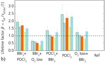
3 Fig. 3. a) Effective charge carrier lifetimes τ eff measured by QSSPC at an injection level Δn = cm -3 for five materials and five high-temperature process sequences as well as the reference group without any high-temperature process. The error bars represent the standard deviation of τ eff measured on three to four samples at five positions each. The measurement positions are exemplarily marked in the first PL image in Fig. 4. b) Lifetime factor β as given in Eq. (1). same level as the group Ref independent of whether there has been a POCl 3 diffusion or process O 2 low before BBr 3 diffusion. The factor β is found to be β 1 for most of the materials or even β 1.3 for Mat1 and Mat5. Only the process sequence BBr 3 + O 2 low significantly reduces τ eff by 0.3 β 0.7 compared with group Ref. This degradation might be correlated with the O 2 low process as for all other combinations with BBr 3 diffusion the factor β is found to be β 1 (see discussion above). A more detailed discussion will follow when discussing the PL images. In the literature, it is reported that BBr 3 diffusion might lead to a significant degradation of τ eff [9]. Here, we demonstrate that our optimized BBr 3 diffusion process is suitable for sequential diffusion processes. In combination with POCl 3 diffusion, τ eff is at least the same as for group Ref, no matter which process order is used. When using sequential diffusion processes with POCl 3 first and then BBr 3, the phosphorus atoms can be drivenin even deeper during the BBr 3 diffusion. Our results indicate that both orders of the two diffusion processes are suitable for cell manufacturing, but for cell concepts that heavily rely on high bulk lifetimes, such as back contact back junction cells, POCl 3 -last processing does appear to be advantageous. Single POCl 3 diffusion as well as POCl 3 -last processing lead to highest β values in this investigation. This might be correlated to a high gettering effect initiated by POCl 3 diffusion. In n-type silicon, impurities as Co, Cr, Ni and Fe might be recombination active and reduce τ eff [10]. Phosphorus gettering is known to reduce these impurities in silicon wafers [11 14]. However, it is Process sequences BBr 3 + POCl 3 BBr 3 + O 2 low POCl 3 + BBr 3 POCl 3 O 2 low + BBr 3 Ref Material Mat1 Mat2 Mat3 Mat4 Mat5 Fig. 4. Photoluminescence (PL) images for the five materials after the indicated high-temperature processes, etch back, passivation, and firing in the first experiment (one representative wafer per group). The PL intensity scale is the same for all images. The reference group Ref is also shown. At the top left PL image, the positions of the performed QSSPC measurements in Fig. 3 and Fig. 5 are exemplarily marked.


.")


4 not clear which type of impurity is relevant for the n-type wafers used in our investigation. However, all materials show the same trends for the different process combinations. Most of the materials and most of the process sequences show τ eff > 1 ms and β 1. Mat4 shows the lowest β for all process sequences compared with the other materials. In comparison with Mat1, Mat2, and Mat5, the content of thermal donors is much higher (see Fig. 2). Thus, the thermal donors might affect τ eff for Mat4. However, the high content of thermal donors for Mat3 does not seem to affect τ eff. In Fig. 4, PL images for the five materials after the high-temperature processes, as indicated in Fig. 3, are shown for one representative wafer per group after firing. Lines with lower PL intensity parallel to the wafer edges are caused by an insufficient saw-damage etching. Other scratches are attributed to wafer handling. The group Ref without any high-temperature processing is also shown in the very right column. As already discussed, the process combination BBr 3 + O 2 low shows a degradation of τ eff for all materials (Fig. 3). This can also be seen from the PL images. Wafers processed with BBr 3 + O 2 low show a dark area with lower PL intensity for all materials (Fig. 4). These dark structures might originate from an interaction of boron dopants and silicon interstitials injected by the O 2 low oxidation causing lower τ eff compared with the reference group Ref. As these dark structures are visible in every material, they might be attributed to the process sequence and not to the material properties. Mat2 and Mat3 show slight ring structures for the process sequence POCl 3 + BBr 3, and Mat3 also for the sequence O 2 low + BBr 3. Such ring structures are typically formed by oxygen precipitate formation [15]. These ring structures seem not to cause a significant degradation of τ eff for Mat2. The QSSPC measurement performed in the wafer s center results in a similar τ eff as the measurements performed at the other four positions. The wafers from Mat3 behave different. The QSSPC measurement in the wafer s center shows about 10% lower τ eff compared to the measurement at the other four positions for both sequences with BBr 3 -last processing. In general, Mat3 with high content of thermal donors behaves similar as Mat1 with marginal content of thermal donors. Only for the process sequences with BBr 3 -last processing small ring defects and a slight degradation of τ eff occur in the wafer s centre for Mat3. But these ring defects are also visible for Mat2 which does hardly contain any thermal donors. Hence, thermal donors do not seem to significantly influence the materials properties after exposure to specific high-temperature processes. 3.3 Experiment 2: high-temperature process sequence variation For Mat1 and Mat2, the influence of the order of high-temperature processes with higher or lower temperature first as well as the applied gas atmosphere on τ eff is investigated in more detail. The used process sequence is the same as in Fig. 1 and the measured τ eff after firing are shown in Fig. 5a). Again, we calculate the lifetime factor β as given in Eq. (1); see Fig. 5b). Again, it is obvious that the POCl 3 diffusion process being the second high temperature process shows an increased τ eff compared with the reference group Ref. The factor β is calculated to be β = 2.6 and β = 1.8 for Mat1 and Mat2, respectively, when O 2 high is the preceding Fig. 5. a) Effective charge carrier lifetimes τ eff measured by QSSPC at an injection level Δn = cm -3 for two materials and the stated eight high-temperature process sequences, including the reference group without any high-temperature process. The error bars represent the standard deviation of τ eff measured on three to four samples at five positions each. The measurement positions are exemplarily marked in the first PL image in Fig. 4. b) Lifetime factor β calculated as given in Eq. (1). Processes O 2 high + POCl Material 3 Mat1 Mat2 POCl 3 + O 2 high POCl 3 + N 2 high Fig. 6. Selected PL images for the two materials Mat1 and Mat2 taken after the indicated high-temperature processes, wet-chemical etch back, passivation and firing in the second experiment (one representative wafer per group). The PL intensity scale is the same as in Fig. 4. high-temperature process. These β values are very similar as those calculated for Mat1 and Mat2 after a single POCl 3 diffusion (see section 3.2). But when N 2 high is the preceding high-temperature process before POCl 3

. The factor β is found to be 0.6 < β < 0.9 for Mat2 while 1.2 < β < 1.6 for Mat1.")

5 diffusion, β is reduced to β = 1.3 for both materials. Thus, the process O 2 high seems advantageous compared to N 2 high within the process sequence with following POCl 3 diffusion. However, most of the process sequences with the high-temperature process at low temperature first and the process at high-temperature second yield 1.3 < β < 2.6, only the sequence N 2 high + N 2 low shows a reduced τ eff with β 0.7 for both materials. The reason for this is not clear yet and further investigations are necessary. Mat2 shows reduced τ eff after process sequences with the higher temperature last (either O 2 or N 2 gas atmosphere). The factor β is found to be 0.6 < β < 0.9 for Mat2 while 1.2 < β < 1.6 for Mat1. The origin can be found in ring-like structures as apparent from the PL images in Fig. 6. For Mat2, O 2 high as well as N 2 high cause dark ring structures when being the second hightemperature process. The PL intensity in the ring area is even lower for O 2 high than for N 2 high. This is not only valid when POCl 3 is the first process but also for the groups with O 2 low + O 2 high or N 2 low + N 2 high (PL images not shown). As already mentioned, such ring structures are typically formed by oxygen precipitate formation [15]. But no ring structures are visible when O 2 high is the first process followed by either POCl 3 diffusion or O 2 low. Furthermore, a lot of point-like structures appear especially for Mat1 after the process sequences featuring N 2 high as first process, as can be seen in the PL images in Fig. 7a) for representative wafers of material Mat1. The point-like structures are obvious for the sequences N 2 high + POCl 3 as well as N 2 high + N 2 low. These point-like structures might be attributed to oxide stacking faults [16]. But as β = 2.6 for Mat1 and the process sequence N 2 high + POCl 3, these point-like structures seem not to necessarily reduce τ eff. When changing the process order to N 2 low + N 2 high, no point-like structures are visible. Fig. 7b) shows the enlargement of the area marked in Fig. 7a). The PL images are taken as-cut, after process N 2 high, after POCl 3 diffusion and finally after passivation and firing. It is obvious that the point-like structures occur right after the N 2 high process. They stay at the same positions after POCl 3 diffusion as well as after passivation and firing. This indicates that the point-like structures can be related to the silicon bulk and not to the surface. The reason for these point-like structures as well as their impact on τ eff need to be further investigated. 4 SUMMARY AND CONCLUSION The present work shows the impact of hightemperature processes at different temperatures, times, and gas atmospheres on n-type Czochralski-grown silicon wafers. Symmetric samples for lifetime measurements have been processed from wafers from five different ingots with different base resistivities and different contents of thermal donors. The high-temperature processes include BBr 3, POCl 3, O 2, or N 2 tube furnace processes, which are typically used for fabrication of high-efficiency n-type silicon solar cells. The five materials react very differently to the hightemperature process sequences. Some process sequences have a positive impact on the effective charge carrier lifetimes τ eff of these wafers, while other wafers show reduced τ eff. a) Process sequences N 2 high + POCl 3 POCl 3 -last processing has a positive impact on τ eff for all materials. This might be related to a POCl 3 gettering that reduces recombination active impurities in the silicon wafers. After single POCl 3 diffusion, this results in 3 ms τ eff 6 ms for all investigated materials. Our optimized BBr 3 diffusion process is suitable for sequential diffusion processes. In combination with POCl 3 diffusion, τ eff is at least the same as for the reference group (no high-temperature processing), no matter which process order is used. For process sequences with a moderate temperature in the first and a high temperature in the second process, some of the investigated wafers show ring structures, which likely originate from oxygen precipitate formation. These materials do not show any ring structures when changing the order of the high-temperature processes. Besides ring structures, also point-like structures are observed for some wafers which are subjected to process sequences with pure N 2 gas atmosphere at 1000 C as first process. These point-like structures might be attributed to oxide stacking faults, but they seem not to necessarily reduce τ eff. An appropriate order of the high temperature processes enables final charge carrier lifetimes that maintain or even exceed the values initially measured without any high-temperature processing. ACKNOWLEDGEMENT N 2 high + N 2 low N 2 low + N 2 high b) Enlargement of the area marked in a) after passivation and as cut after N 2 high after POCl 3 firing Fig. 7. a) Selected PL images for the material Mat1 taken after the indicated high-temperature process sequences, wet-chemical etch back, passivation, and firing in the second experiment (one representative wafer per group). The PL intensity scale is the same as in Fig. 4 and Fig. 6. b) Enlargement of the area marked in a). The PL images are taken as-cut, directly after the N 2 high tube furnace process, after POCl 3 diffusion and finally after passivation and firing. Different PL systems are used and the scaling is different. The authors would like to thank all colleagues at the Fraunhofer ISE Photovoltaic Technology Evaluation
6 Center (PV-TEC), especially U. Belledin, S. Maier and J. Stoffel. lifetime in n-type silicon", J. Appl. Phys., vol. 118, no. 21, p , REFERENCES [1] K. Bothe, R. Sinton, J. Schmidt, "Fundamental boron-oxygen-related carrier lifetime limit in monoand multicrystalline silicon", Prog. Photovolt.: Res. Appl., vol. 13, pp , [2] A. Usami, Y. Fujii, K. Monoka, "The effect of swirl defects on the minority carrier lifetime in heattreated silicon crystals", J. Phys. D: Appl. Phys., vol. 10, no. 6, pp , [3] S. Werner, E. Lohmüller, S. Maier et al., "Process optimization for the front side of p-type silicon solar cells", Proc. 29th EU PVSEC, Amsterdam, Netherlands, 2014, pp [4] A. Wolf, A. Kimmerle, S. Werner et al., "Status and perspective of emitter formation by POCl 3 - diffusion", Proc. 31st EU PVSEC, Hamburg, Germany, 2015, pp [5] S. Werner, E. Lohmüller, U. Belledin et al., "Optimization of BBr 3 diffusion processes for n- type silicon solar cells", Proc. 31st EU PVSEC, Hamburg, Germany, 2015, pp [6] M. Spitz, U. Belledin, S. Rein, "Fast inductive inline measurement of the emitter sheet resistance in industrial solar cell fabrication", Proc. 22nd EU PVSEC, Milan, Italy, 2007, pp [7] Seiffe J., Weiss L., Hofmann M. et al., "Alternative rear surface passivation for industrial cell production", Proc. 23rd EU PVSEC, Valencia, Spain, [8] R. C. Newman, "Thermal donors in silicon: oxygen clusters or self-interstitial aggregates", J. Phys. C: Solid State Phys. (Journal of Physics C: Solid State Physics), vol. 18, no. 30, pp , [9] M. A. Kessler, T. Ohrdes, B. Wolpensinger et al., "Charge carrier lifetime degradation in Cz silicon through the formation of a boron-rich layer during BBr 3 diffusion processes", Semiconductor Science and Technology, vol. 25, no. 5, pp. 1 9, [10] J. Schmidt, B. Lim, D. Walter et al., "Impurityrelated limitations of next-generation industrial silicon solar cells", IEEE J. Photovoltaics, vol. 3, no. 1, pp , [11] S. M. Myers, M. Seibt, W. Schröter, "Mechanisms of transition-metal gettering in silicon", J. Appl. Phys., vol. 88, no. 7, pp , [12] M. Seibt, A. Sattler, C. Rudolf et al., "Gettering in silicon photovoltaics: current state and future perspectives", phys. stat. sol. (a), vol. 203, no. 4, pp , [13] M. B. Shabani, T. Yamashita, E. Morita, "Metallic impurities in mono and multi-crystalline silicon and their gettering by phosphorus diffusion", 214th ECS Meeting, Honolulu, HI, 2008, pp [14] J. Schön, H. Habenicht, W. Warta et al., "Chromium distribution in multicrystalline silicon: comparison of simulations and experiments", Prog. Photovolt: Res. Appl., pp , [15] A. Borghesi, B. Pivac, A. Sassella et al., "Oxygen precipitation in silicon", J. Appl. Phys., vol. 77, no. 9, pp , [16] J. D. Murphy, M. Al-Amin, K. Bothe et al., "The effect of oxide precipitates on minority carrier
Presented at the 29th European PV Solar Energy Conference and Exhibition, September 2014, Amsterdam (NL)
") POCL3-BASED CO-DIFFUSION PROCESS FOR N-TYPE BACK-CONTACT BACK-JUNCTION SOLAR CELLS R. Keding 1,2, M. Hendrichs 1, D.Stüwe 1, M. Jahn 1, C. Reichel 1, D. Borchert 1, A.Wolf 1, H. Reinecke 3, D.Biro 1 1
POCL3-BASED CO-DIFFUSION PROCESS FOR N-TYPE BACK-CONTACT BACK-JUNCTION SOLAR CELLS R. Keding 1,2, M. Hendrichs 1, D.Stüwe 1, M. Jahn 1, C. Reichel 1, D. Borchert 1, A.Wolf 1, H. Reinecke 3, D.Biro 1 1
HIGH EFFICIENCY INDUSTRIAL SCREEN PRINTED N-TYPE SOLAR CELLS WITH FRONT BORON EMITTER
 HIGH EFFICIENCY INDUSTRIAL SCREEN PRINTED N-TYPE SOLAR CELLS WITH FRONT BORON EMITTER V.D. Mihailetchi 1, Y. Komatsu 1, G. Coletti 1, R. Kvande 2, L. Arnberg 2, C. Knopf 3, K. Wambach 3, L.J. Geerligs
Available online at ScienceDirect. Energy Procedia 55 (2014 )
") Available online at www.sciencedirect.com ScienceDirect Energy Procedia 55 (2014 ) 287 294 4th International Conference on Silicon Photovoltaics, SiliconPV 2014 Codiffused bifacial n-type solar cells (CoBiN)
Available online at www.sciencedirect.com ScienceDirect Energy Procedia 55 (2014 ) 287 294 4th International Conference on Silicon Photovoltaics, SiliconPV 2014 Codiffused bifacial n-type solar cells (CoBiN)
Abstract. Introduction
 Light Induced Degradation in Manufacturable Multi-crystalline Silicon Solar Cells Ben Damiani, Mohamed Hilali, and Ajeet Rohatgi University Center of Excellence for Photovoltaics Research Georgia Institute
RECORD EFFICIENCIES OF SOLAR CELLS BASED ON N-TYPE MULTICRYSTALLINE SILICON. Center, ISC-Konstanz, Rudolf-Diesel-Str. 15, D Konstanz, Germany
 RECORD EFFICIENCIES OF SOLAR CELLS BASED ON N-TYPE MULTICRYSTALLINE SILICON J. Libal *, R. Kopecek +, I. Roever, K. Wambach * University of Konstanz, Faculty of Sciences, Department of Physics, now at
24th European Photovoltaic Solar Energy Conference and Exhibition, September 2009, Hamburg, Germany.
 STATUS OF N-TYPE SOLAR CELLS FOR LOW-COST INDUSTRIAL PRODUCTION Arthur Weeber*, Ronald Naber, Nicolas Guillevin, Paul Barton, Anna Carr, Desislava Saynova, Teun Burgers, Bart Geerligs ECN Solar Energy,
N-PERT BACK JUNCTION SOLAR CELLS: AN OPTION FOR THE NEXT INDUSTRIAL TECHNOLOGY GENERATION?
 N-PERT BACK JUNCTION SOLAR CELLS: AN OPTION FOR THE NEXT INDUSTRIAL TECHNOLOGY GENERATION? Bianca Lim *, Till Brendemühl, Miriam Berger, Anja Christ, Thorsten Dullweber Institute for Solar Energy Research
Available online at ScienceDirect. Energy Procedia 77 (2015 )
") Available online at www.sciencedirect.com ScienceDirect Energy Procedia 77 (2015 ) 279 285 5th International Conference on Silicon Photovoltaics, SiliconPV 2015 21%-Efficient n-type rear-junction PERT
Available online at www.sciencedirect.com ScienceDirect Energy Procedia 77 (2015 ) 279 285 5th International Conference on Silicon Photovoltaics, SiliconPV 2015 21%-Efficient n-type rear-junction PERT
INDUSTRIALLY FEASIBLE >19% EFFICIENCY IBC CELLS FOR PILOT LINE PROCESSING
 INDUSTRIALLY FEASIBLE >19% EFFICIENCY IBC CELLS FOR PILOT LINE PROCESSING F. J. Castaño 1, D. Morecroft 1, M. Cascant 1, H. Yuste 1, M.W.P.E. Lamers 2, A.A. Mewe 2, I.G. Romijn 2, E.E. Bende 2, Y. Komatsu
Available online at ScienceDirect. Energy Procedia 92 (2016 )
") Available online at www.sciencedirect.com ScienceDirect Energy Procedia 92 (2016 ) 925 931 6th International Conference on Silicon Photovoltaics, SiliconPV 2016 Contacting BBr 3 -based boron emitters with
Available online at www.sciencedirect.com ScienceDirect Energy Procedia 92 (2016 ) 925 931 6th International Conference on Silicon Photovoltaics, SiliconPV 2016 Contacting BBr 3 -based boron emitters with
Solar Energy Research Institute of Singapore (SERIS), National University of Singapore (NUS), Singapore
, National University of Singapore (NUS), Singapore") MODELLING AND CHARACTERIZATION OF BBr3 BORON DIFFUSION PROCESS FOR N-TYPE SI WAFER SOLAR CELLS LI Mengjie 1, 2, a, HOEX Bram 3, MA Fa-Jun 3, DEVAPPA SHETTY Kishan 1, ABERLE Armin G. 1, 2, SAMUDRA Ganesh
MODELLING AND CHARACTERIZATION OF BBr3 BORON DIFFUSION PROCESS FOR N-TYPE SI WAFER SOLAR CELLS LI Mengjie 1, 2, a, HOEX Bram 3, MA Fa-Jun 3, DEVAPPA SHETTY Kishan 1, ABERLE Armin G. 1, 2, SAMUDRA Ganesh
Inductive Coupled Plasma (ICP) Textures as Alternative for Wet Chemical Etching in Solar Cell Fabrication
 Textures as Alternative for Wet Chemical Etching in Solar Cell Fabrication") Inductive Coupled Plasma (ICP) Textures as Alternative for Wet Chemical Etching in Solar Cell Fabrication 1 Motivation 2 Experimental setup 3 ICP textures as alternative technique 3.1 Surface morphology
Inductive Coupled Plasma (ICP) Textures as Alternative for Wet Chemical Etching in Solar Cell Fabrication 1 Motivation 2 Experimental setup 3 ICP textures as alternative technique 3.1 Surface morphology
1 INTRODUCTION 2 EXPERIMENTATION
 COMPARISON OF POCL 3 & BBR 3 FURNACE DIFFUSSION DOPANT SOURCES TO PHOSPHORUS & BORON IMPLANT AND PLASMA DOPANT SOURCES FOR SELECTIVE EMITTER FORMATION USING LOCALIZED LASER MELT (LLM) ANNEALING EITHER
Citation for the original published paper (version of record):
:") http://www.diva-portal.org This is the published version of a paper published in Energy Procedia. Citation for the original published paper (version of record): Boulfrad, Y., Lindroos, J., Inglese, A.,
http://www.diva-portal.org This is the published version of a paper published in Energy Procedia. Citation for the original published paper (version of record): Boulfrad, Y., Lindroos, J., Inglese, A.,
TWO-DIMENSIONAL MODELING OF EWT MULTICRYSTALLINE SILICON SOLAR CELLS AND COMPARISON WITH THE IBC SOLAR CELL
 TWO-DIMENSIONAL MODELING OF EWT MULTICRYSTALLINE SILICON SOLAR CELLS AND COMPARISON WITH THE IBC SOLAR CELL Mohamed M. Hilali, Peter Hacke, and James M. Gee Advent Solar, Inc. 8 Bradbury Drive S.E, Suite,
22nd European Photovoltaic Solar Energy Conference, 3-7 September 2007, Milan, Italy
 EFFECT OF IMPURITIES ON THE MINORITY CARRIER LIFETIME OF SILICON MADE BY THE METALLURGICAL ROUTE Arve Holt 1, Erik Enebakk 2 and Anne-Karin Soiland 2 1 Institute for Energy Technology, P.O. Box 24, NO-2027
Surface Preparation Challenges in Crystalline Silicon Photovoltaic Manufacturing
 Surface Preparation Challenges in Crystalline Silicon Photovoltaic Manufacturing Kristopher Davis 1,3, Andrew C. Rudack 2,3, Winston Schoenfeld 1,3 Hubert Seigneur 1,3, Joe Walters 1,3, Linda Wilson 2,3
Advances in PassDop technology: recombination and optics
 Available online at www.sciencedirect.com ScienceDirect Energy Procedia 124 (2017) 313 320 www.elsevier.com/locate/procedia 7th International Conference on Silicon Photovoltaics, SiliconPV 2017 Advances
Available online at ScienceDirect. Energy Procedia 55 (2014 )
") Available online at www.sciencedirect.com ScienceDirect Energy Procedia 55 (2014 ) 618 623 4th International Conference on Silicon Photovoltaics, SiliconPV 2014 Cast silicon of varying purity for high
Available online at www.sciencedirect.com ScienceDirect Energy Procedia 55 (2014 ) 618 623 4th International Conference on Silicon Photovoltaics, SiliconPV 2014 Cast silicon of varying purity for high
Publication I American Institute of Physics (AIP) Reprinted by permission of American Institute of Physics.
 Reprinted by permission of American Institute of Physics.") Publication I H. Talvitie, V. Vähänissi, A. Haarahiltunen, M. Yli-Koski, and H. Savin. 2011. Phosphorus and boron diffusion gettering of iron in monocrystalline silicon. Journal of Applied Physics, volume
Publication I H. Talvitie, V. Vähänissi, A. Haarahiltunen, M. Yli-Koski, and H. Savin. 2011. Phosphorus and boron diffusion gettering of iron in monocrystalline silicon. Journal of Applied Physics, volume
Anodic Aluminium Oxide for Passivation in Silicon Solar Cells
 Anodic Aluminium Oxide for Passivation in Silicon Solar Cells School of Photovoltaic & Renewable Energy Engineering Zhong Lu Supervisor: Alison Lennon May. 2015 Co-supervisor: Stuart Wenham Outline Introduction
31st European Photovoltaic Solar Energy Conference and Exhibition APPLICATIONS OF CARRIER DE-SMEARING OF PHOTOLUMINESCENCE IMAGES ON SILICON WAFERS
 This is a pre-peer review version of the paper submitted to the ournal Progress in Photovoltaics. APPLICATIONS OF CARRIER DE-SMEARING OF PHOTOLUMINESCENCE IMAGES ON SILICON WAFERS S. P. Phang, H. C. Sio,
HOMEWORK 4 and 5. March 15, Homework is due on Monday March 30, 2009 in Class. Answer the following questions from the Course Textbook:
 HOMEWORK 4 and 5 March 15, 2009 Homework is due on Monday March 30, 2009 in Class. Chapter 7 Answer the following questions from the Course Textbook: 7.2, 7.3, 7.4, 7.5, 7.6*, 7.7, 7.9*, 7.10*, 7.16, 7.17*,
REAR SURFACE PASSIVATION OF INTERDIGITATED BACK CONTACT SILICON HETEROJUNCTION SOLAR CELL AND 2D SIMULATION STUDY
 REAR SURFACE PASSIVATION OF INTERDIGITATED BACK CONTACT SILICON HETEROJUNCTION SOLAR CELL AND 2D SIMULATION STUDY Meijun Lu 1,2, Ujjwal Das 1, Stuart Bowden 1, and Robert Birkmire 1,2 1 Institute of Energy
Metallization Workshop 5 th workshop on metallization of crystalline solar cells 2014
 Metallization Workshop 5 th workshop on metallization of crystalline solar cells 2014 Combined microstructural and electrical characterization of metallization layers in industrial solar cells P. Kumar,
HF last passivation for high efficiency a-si:h/c-si heterojunction solar cells
 HF last passivation for high efficiency a-si:h/c-si heterojunction solar cells Adrien Danel, F. Souche, PJ. Ribeyron : INES Y. Le Tiec : LETI T. Nolan : Akrion Systems 1 A. Danel, UCPSS 20-1 Heterojonction
This is an electronic reprint of the original article. This reprint may differ from the original in pagination and typographic detail.
 Powered by TCPDF (www.tcpdf.org) This is an electronic reprint of the original article. This reprint may differ from the original in pagination and typographic detail. Talvitie, Heli; Vähänissi, Ville;
High Efficiency Multicrystalline Silicon Solar Cells: Potential of n-type Doping
 (c) 215 IEEE. DOI: 1.119/JPHOTOV.215.2466474. Personal use of this material is permitted. Permission from IEEE must be obtained for all other users, including reprinting/ republishing this material 1 High
Turn-key Production System for Solar Cells
 SOLARE Turn-key Production System for Solar Cells 02 Innovations for New Technologies provides technology solutions for both crystalline and thin-film highperformance solar cell platforms. Our production
Implant-cleave process enables ultra-thin wafers without kerf loss
 Implant-cleave process enables ultra-thin wafers without kerf loss Close Alessandro Fujisaka, Sien Kang, Lu Tian, Yi-Lei Chow, Anton Belyaev, Silicon Genesis Corporation, San Jose CA USA The recent shortage
Fabrication Technology
 Fabrication Technology By B.G.Balagangadhar Department of Electronics and Communication Ghousia College of Engineering, Ramanagaram 1 OUTLINE Introduction Why Silicon The purity of Silicon Czochralski
2. High Efficiency Crystalline Si Solar Cells
 2 High Efficiency Crystalline Si Solar Cells Students: Karthick Murukesan, Sandeep S S, Meenakshi Bhaisare, Bandana Singha, Kalaivani S and Ketan Warikoo Faculty members: Anil Kottantharayil, B M Arora,
Review Article High-Efficiency Crystalline Silicon Solar Cells
 Advances in OptoElectronics Volume 2007, Article ID 97370, 15 pages doi:10.1155/2007/97370 Review Article High-Efficiency Crystalline Silicon Solar Cells S. W. Glunz Fraunhofer Institute for Solar Energy
Chapter 3 Silicon Device Fabrication Technology
 Chapter 3 Silicon Device Fabrication Technology Over 10 15 transistors (or 100,000 for every person in the world) are manufactured every year. VLSI (Very Large Scale Integration) ULSI (Ultra Large Scale
EFFECT OF EXTENDED DEFECTS ON THE ELECTRICAL PROPERTIES OF COMPENSATED SOLAR GRADE MULTICRYSTALLINE SILICON
 EFFECT OF EXTENDED DEFECTS ON THE ELECTRICAL PROPERTIES OF COMPENSATED SOLAR GRADE MULTICRYSTALLINE SILICON J. Libal *, M. Acciarri *, S. Binetti *, R. Kopecek, R. Petres, C. Knopf +, K. Wambach + * University
p-si Industrial Application of Uncapped Al 2 O 3 and Firing-Through Al-BSF In Open Rear Passivated Solar Cells ARC SiN x Ag contacts n ++ p ++ Al-BSF
 Industrial Application of Uncapped Al 2 O 3 and Firing-Through Al-BSF In Open Rear Passivated Solar Cells I. Cesar 1, E. Granneman 2, P. Vermont 2, H. Khatri 3, H. Kerp 3, A. Shaikh 3, P. Manshanden 1,
Development of High Efficiency SHJ/Poly-Si Passivating
 Master of Science Thesis Development of High Efficiency SHJ/Poly-Si Passivating Contact Hybrid Solar Cells Hao Ge Development of High Efficiency SHJ/Poly-Si Passivating Contact Hybrid Solar Cells A thesis
Crystalline Silicon Solar Cells Future Directions. Stuart Bowden BAPVC January Stuart Bowden BAPVC January 12,
 Crystalline Silicon Solar Cells Future Directions Stuart Bowden BAPVC January 2011 Stuart Bowden BAPVC January 12, 2011 1 Stuart Bowden Co-Director of Solar Power Labs at ASU Work relevant to BAPVC: Pilot
Lecture 22: Integrated circuit fabrication
 Lecture 22: Integrated circuit fabrication Contents 1 Introduction 1 2 Layering 4 3 Patterning 7 4 Doping 8 4.1 Thermal diffusion......................... 10 4.2 Ion implantation.........................
Solar cell performance prediction using advanced analysis methods on optical images of as-cut wafers
 Available online at www.sciencedirect.com Energy Procedia 00 (2013) 000 000 www.elsevier.com/locate/procedia SiliconPV: March 25-27, 2013, Hamelin, Germany Solar cell performance prediction using advanced
12.2 Silicon Solar Cells
 12.2 Silicon Solar Cells 12.2.1. High Efficiency Crystalline Solar Cells Fabrication of large area (5 inch X 5 inch) crystalline silicon solar cells (S. Saravanan, Karthick Murukesan, Balraj Arunachalam,
Device Architecture and Lifetime Requirements for High Efficiency Multicrystalline Silicon Solar Cells
 Device Architecture and Lifetime Requirements for High Efficiency Multicrystalline Silicon Solar Cells The MIT Faculty has made this article openly available. Please share how this access benefits you.
"Plasma CVD passivation; Key to high efficiency silicon solar cells",
 "Plasma CVD passivation; Key to high efficiency silicon solar cells", David Tanner Date: May 7, 2015 2012 GTAT Corporation. All rights reserved. Summary: Remarkable efficiency improvements of silicon solar
Formation and Annihilation of Hydrogen-Related Donor States in Proton-Implanted and Subsequently Plasma-Hydrogenated N-Type Float-Zone Silicon
 Formation and Annihilation of Hydrogen-Related Donor States in Proton-Implanted and Subsequently Plasma-Hydrogenated N-Type Float-Zone Silicon Reinhart Job, University of Hagen, Germany Franz-Josef Niedernostheide,
Erschienen in: Energy Procedia ; 77 (2015). - S https://dx.doi.org/ /j.egypro Available online at
. - S https://dx.doi.org/ /j.egypro Available online at") Erschienen in: Energy Procedia ; 77 (2015). - S. 75-82 https://dx.doi.org/10.1016/j.egypro.2015.07.012 Available online at www.sciencedirect.com ScienceDirect Energy Procedia 77 (2015 ) 75 82 5th International
Erschienen in: Energy Procedia ; 77 (2015). - S. 75-82 https://dx.doi.org/10.1016/j.egypro.2015.07.012 Available online at www.sciencedirect.com ScienceDirect Energy Procedia 77 (2015 ) 75 82 5th International
Kerf! Microns. Driving Forces Impact of kerf is substantial in terms of silicon usage 50 % of total thickness for 100 mm wafers
 2nd. Annual c-si PVMC Workshop at Intersolar NA, San Francisco, CA, July 2013 1 Microns Kerf! Driving Forces Impact of kerf is substantial in terms of silicon usage 50 % of total thickness for 100 mm wafers
Semiconductor Technology
 Semiconductor Technology from A to Z Oxidation www.halbleiter.org Contents Contents List of Figures List of Tables II III 1 Oxidation 1 1.1 Overview..................................... 1 1.1.1 Application...............................
R Sensor resistance (Ω) ρ Specific resistivity of bulk Silicon (Ω cm) d Diameter of measuring point (cm)
 ρ Specific resistivity of bulk Silicon (Ω cm) d Diameter of measuring point (cm)") 4 Silicon Temperature Sensors 4.1 Introduction The KTY temperature sensor developed by Infineon Technologies is based on the principle of the Spreading Resistance. The expression Spreading Resistance derives
4 Silicon Temperature Sensors 4.1 Introduction The KTY temperature sensor developed by Infineon Technologies is based on the principle of the Spreading Resistance. The expression Spreading Resistance derives
WET-CHEMICAL TREATMENT OF SOLAR GRADE CZ SILICON PRIOR TO SURFACE PASSIVATION
 WET-CHEMICAL TREATMENT OF SOLAR GRADE CZ SILICON PRIOR TO SURFACE PASSIVATION A. Laades 1*, J. Brauer 1, U. Stürzebecher 1, K. Neckermann 1, K. Klimm 2, M. Blech 1, K. Lauer 1, A. Lawerenz 1, H. Angermann
EE40 Lec 22. IC Fabrication Technology. Prof. Nathan Cheung 11/19/2009
 Suggested Reading EE40 Lec 22 IC Fabrication Technology Prof. Nathan Cheung 11/19/2009 300mm Fab Tour http://www-03.ibm.com/technology/manufacturing/technology_tour_300mm_foundry.html Overview of IC Technology
Figure 2.3 (cont., p. 60) (e) Block diagram of Pentium 4 processor with 42 million transistors (2000). [Courtesy Intel Corporation.
 (e) Block diagram of Pentium 4 processor with 42 million transistors (2000). [Courtesy Intel Corporation.") Figure 2.1 (p. 58) Basic fabrication steps in the silicon planar process: (a) oxide formation, (b) selective oxide removal, (c) deposition of dopant atoms on wafer, (d) diffusion of dopant atoms into exposed
Figure 2.1 (p. 58) Basic fabrication steps in the silicon planar process: (a) oxide formation, (b) selective oxide removal, (c) deposition of dopant atoms on wafer, (d) diffusion of dopant atoms into exposed
IMPACT OF FIRING TEMPERATURE PROFILES ON LOCAL BSF FORMATION IN PERC SOLAR CELLS
 IMPACT OF FIRING TEMPERATURE PROFILES ON LOCAL BSF FORMATION IN PERC SOLAR CELLS S. Mack1, P. Richter2, S. Werner1, F. Clement1, A. Wolf1 1Fraunhofer-Institute for Solar Energy Systems ISE 2BTU International
Process Flow in Cross Sections
 Process Flow in Cross Sections Process (simplified) 0. Clean wafer in nasty acids (HF, HNO 3, H 2 SO 4,...) --> wear gloves! 1. Grow 500 nm of SiO 2 (by putting the wafer in a furnace with O 2 2. Coat
Effect of external gettering with porous silicon on the electrical properties of Metal-Oxide-Silicon devices
 Available online at www.sciencedirect.com www.elsevier.com/locate/xxx Physics Physics Procedia 2 (2009) (2008) 983 988 000 000 www.elsevier.com/locate/procedia Proceedings of the JMSM 2008 Conference Effect
Schottky-barrier and MIS solar cells
 Schottky-barrier and MIS solar cells (Metal-Insulator- Semiconductor) Steve Byrnes NSE 290 Final Presentation December 1, 2008 Outline Background on Schottky barriers Dark and light I-V curves, and effect
Chapter 2 MOS Fabrication Technology
 Chapter 2 MOS Fabrication Technology Abstract This chapter is concerned with the fabrication of metal oxide semiconductor (MOS) technology. Various processes such as wafer fabrication, oxidation, mask
Materials Characterization
 Materials Characterization C. R. Abernathy, B. Gila, K. Jones Cathodoluminescence (CL) system FEI Nova NanoSEM (FEG source) with: EDAX Apollo silicon drift detector (TE cooled) Gatan MonoCL3+ FEI SEM arrived
Screen Printed Al-Pastes for LFC Solar Cells
 Screen Printed Al-Pastes for LFC Solar Cells C. Schwab 1, B. Thaidigsmann 1, M. Linse 1, A. Wolf 1, F. Clement 1, A. Prince 2, R. Young 2, P. Weigand 3 1 Fraunhofer Institute for Solar Energy Systems ISE
Passivation of silicon wafers by Silicon Carbide (SiC x ) thin film grown by sputtering
 thin film grown by sputtering") Available online at www.sciencedirect.com Energy Procedia 10 (2011 ) 71 75 European Materials Research Society Conference Symp. Advanced Inorganic Materials and Concepts for Photovoltaics Passivation of
Available online at www.sciencedirect.com Energy Procedia 10 (2011 ) 71 75 European Materials Research Society Conference Symp. Advanced Inorganic Materials and Concepts for Photovoltaics Passivation of
27th European Photovoltaic Solar Energy Conference and Exhibition ANALYSIS OF MONO-CAST SILICON WAFER AND SOLAR CELLS
 ANALYSIS OF MONO-CAST SILICON WAFER AND SOLAR CELLS Kai Petter* 1, Thomas Kaden 2, Ronny Bakowskie 1, Yvonne Ludwig 1, Ronny Lantzsch 1, Daniel Raschke 1, Stephan Rupp 1, Thomas Spiess 1 1 Q-Cells SE,
Ion Implantation Most modern devices doped using ion implanters Ionize gas sources (single +, 2+ or 3+ ionization) Accelerate dopant ions to very
 Accelerate dopant ions to very") Ion Implantation Most modern devices doped using ion implanters Ionize gas sources (single +, 2+ or 3+ ionization) Accelerate dopant ions to very high voltages (10-600 KeV) Use analyzer to selection charge/mass
Ion Implantation Most modern devices doped using ion implanters Ionize gas sources (single +, 2+ or 3+ ionization) Accelerate dopant ions to very high voltages (10-600 KeV) Use analyzer to selection charge/mass
a-sin x :H Antireflective And Passivation Layer Deposited By Atmospheric Pressure Plasma
 Vailable online at www.sciencedirect.com Energy Procedia 27 (2012 ) 365 371 SiliconPV: April 03-05, 2012, Leuven, Belgium a-sin x :H Antireflective And Passivation Layer Deposited By Atmospheric Pressure
THERMAL OXIDATION - Chapter 6 Basic Concepts
 THERMAL OXIDATION - Chapter 6 Basic Concepts SiO 2 and the Si/SiO 2 interface are the principal reasons for silicon s dominance in the IC industry. Oxide Thickness µm 0. µm 0 nm nm Thermally Grown Oxides
Surface micromachining and Process flow part 1
 Surface micromachining and Process flow part 1 Identify the basic steps of a generic surface micromachining process Identify the critical requirements needed to create a MEMS using surface micromachining
Ajay Kumar Gautam [VLSI TECHNOLOGY] VLSI Technology for 3RD Year ECE/EEE Uttarakhand Technical University
![Ajay Kumar Gautam [VLSI TECHNOLOGY] VLSI Technology for 3RD Year ECE/EEE Uttarakhand Technical University](/thumbs/75/72824557.jpg "Ajay Kumar Gautam [VLSI TECHNOLOGY] VLSI Technology for 3RD Year ECE/EEE Uttarakhand Technical University") 2014 Ajay Kumar Gautam [VLSI TECHNOLOGY] VLSI Technology for 3RD Year ECE/EEE Uttarakhand Technical University Page1 Syllabus UNIT 1 Introduction to VLSI Technology: Classification of ICs, Scale of integration,
2014 Ajay Kumar Gautam [VLSI TECHNOLOGY] VLSI Technology for 3RD Year ECE/EEE Uttarakhand Technical University Page1 Syllabus UNIT 1 Introduction to VLSI Technology: Classification of ICs, Scale of integration,
Fig 1.1 Band Gap for Six-Junction Tandem Stack
 This research was, in part, funded by the U.S. Government. The views and conclusions contained in this document are those of the authors and should not be interpreted as representing the official policies,
Simulation of device parameters of high efficiency multicrystalline silicon solar cells
 Volume 1 Issue EMR1 ice science Pages 32 http://dx.doi.org/10.1680/emr.11.00007 Research Article Received 06/09/2011 Accepted 08/11/2011 Published online 10/11/2011 Keywords: /device simulation/silicon
All-Aluminum Screen-Printed IBC Cells: Design Concept
 l-uminum Screen-Printed IBC Cells: Design Concept Paul Basore, Emmanuel Van Kerschaver, Kirsten Cabanas-Holmen, Jean Hummel, Yafu Lin, C Paola Murcia, Kate Fisher, Simeon Baker-Finch, Oun-Ho Park, Frederic
Silicon Wafer Processing PAKAGING AND TEST
 Silicon Wafer Processing PAKAGING AND TEST Parametrical test using test structures regularly distributed in the wafer Wafer die test marking defective dies dies separation die fixing (not marked as defective)
A discussion of crystal growth, lithography, etching, doping, and device structures is presented in
 Chapter 5 PROCESSING OF DEVICES A discussion of crystal growth, lithography, etching, doping, and device structures is presented in the following overview gures. SEMICONDUCTOR DEVICE PROCESSING: AN OVERVIEW
Materials, Electronics and Renewable Energy
 Materials, Electronics and Renewable Energy Neil Greenham ncg11@cam.ac.uk Inorganic semiconductor solar cells Current-Voltage characteristic for photovoltaic semiconductor electrodes light Must specify
EECS130 Integrated Circuit Devices
 EECS130 Integrated Circuit Devices Professor Ali Javey 9/13/2007 Fabrication Technology Lecture 1 Silicon Device Fabrication Technology Over 10 15 transistors (or 100,000 for every person in the world)
1. Introduction. What is implantation? Advantages
 Ion implantation Contents 1. Introduction 2. Ion range 3. implantation profiles 4. ion channeling 5. ion implantation-induced damage 6. annealing behavior of the damage 7. process consideration 8. comparison
23rd European Photovoltaic Solar Energy Conference, 1-5 September 2008, Valencia, Spain
 TEXTURED SILICON HETEROJUNCTION SOLAR CELLS WITH OVER 700 MV OPEN-CIRCUIT VOLTAGE STUDIED BY TRANSMISSION ELECTRON MICROSCOPY S. Olibet 1*, C. Monachon 1,2, A. Hessler-Wyser 2, E. Vallat-Sauvain 1+, S.
Solid State Phenomena Vols (2014) pp (2014) Trans Tech Publications, Switzerland doi: /www.scientific.net/ssp
 pp (2014) Trans Tech Publications, Switzerland doi: /www.scientific.net/ssp") Solid State Phenomena Vols. 205-206 (2014) pp 118-127 (2014) Trans Tech Publications Switzerland doi:10.4028/www.scientific.net/ssp.205-206.118!"#"$!#"%& '(')"(!*&$+*$-./#(0$$(1*$ %$!'!' /$ *)"( /2&34
Solid State Phenomena Vols. 205-206 (2014) pp 118-127 (2014) Trans Tech Publications Switzerland doi:10.4028/www.scientific.net/ssp.205-206.118!"#"$!#"%& '(')"(!*&$+*$-./#(0$$(1*$ %$!'!' /$ *)"( /2&34
Available online at ScienceDirect. Energy Procedia 55 (2014 )
") Available online at www.sciencedirect.com ScienceDirect Energy Procedia 55 (2014 ) 702 707 4th International Conference on Silicon Photovoltaics, SiliconPV 2014 Observation of the contact formation of
Available online at www.sciencedirect.com ScienceDirect Energy Procedia 55 (2014 ) 702 707 4th International Conference on Silicon Photovoltaics, SiliconPV 2014 Observation of the contact formation of
OPTICAL, ELECTRICAL AND STRUCTURAL PROPERTIES OF PECVD QUASI EPITAXIAL PHOSPHOROUS DOPED SILICON FILMS ON CRYSTALLINE SILICON SUBSTRATE
 OPTICAL, ELECTRICAL AN STRUCTURAL PROPERTIES OF PECV QUASI EPITAXIAL PHOSPHOROUS OPE SILICON FILMS ON CRYSTALLINE SILICON SUBSTRATE Mahdi Farrokh-Baroughi, Hassan El-Gohary, and Siva Sivoththaman epartment
Quality requirements for wafers, cells and PV modules
 Outdoor test-site PI Berlin Quality requirements for wafers, cells and PV modules Intersolar 2008 in Munich, 12th of June 2008 Stefan Krauter, Paul Grunow, Sven Lehmann PI Photovoltaik-Institut Berlin
Application of infrared thermography to the characterization of multicristalline silicon solar cells
 Application of infrared thermography to the characterization of multicristalline silicon solar cells A. Kaminski, O. Nichiporuk*, J. Jouglar, P.L. Vuillermoz, A. Laugier Laboratoire de Physique de la Matière
ELEC 3908, Physical Electronics, Lecture 4. Basic Integrated Circuit Processing
 ELEC 3908, Physical Electronics, Lecture 4 Basic Integrated Circuit Processing Lecture Outline Details of the physical structure of devices will be very important in developing models for electrical behavior
Boron Diffusion and Silicon Self-Interstitial Recycling between SiGeC layers
 Mat. Res. Soc. Symp. Proc. Vol. 810 2004 Materials Research Society C3.5.1 oron Diffusion and Silicon Self-Interstitial Recycling between SiGeC layers M. S. Carroll 1 J. C. Sturm, Dept. of Electrical Engineering,
csi PRODUCTION SOLUTIONS csi PRODUCTION SOLUTIONS FOR CRYSTALLINE SILICON SOLAR CELLS
 csi PRODUCTION csi PRODUCTION FOR CRYSTALLINE SILICON SOLAR CELLS 3 PASSION FOR EFFICIENCY PHOTOVOLTAICS CONTENT Process machines and automation systems by Manz offer many advantages for customers in the
ETIP-PV Manufacturing Conference Brussels, May 19 th Epitaxial Wafers: A game-changing technology on its way to mass production
 ETIP-PV Manufacturing Conference Brussels, May 19 th 2017 Epitaxial Wafers: A game-changing technology on its way to mass production NexWafe: producer of high-quality silicon wafers NexWafe will supply
EE 330 Lecture 9. IC Fabrication Technology Part II. -Oxidation -Epitaxy -Polysilicon -Planarization -Resistance and Capacitance in Interconnects
 EE 330 Lecture 9 IC Fabrication Technology Part II -Oxidation -Epitaxy -Polysilicon -Planarization -Resistance and Capacitance in Interconnects Review from Last Time Etching Dry etch (anisotropic) SiO
2007 Elsevier Science. Reprinted with permission from Elsevier.
 J. Härkönen, E. Tuovinen, P. Luukka, H.K. Nordlund, and E. Tuominen, Magnetic Czochralski silicon as detector material, Nuclear Instruments and Methods in Physics Research A 579 (2007) 648 652. 2007 Elsevier
Single-Seed Casting Large-Size Monocrystalline Silicon for High-Efficiency and Low-Cost Solar Cells
 Research Advanced Materials Article Engineering 2015, 1(3): 378 383 DOI 10.15302/J-ENG-2015032 Single-Seed Casting Large-Size Monocrystalline Silicon for High-Efficiency and Low-Cost Solar Cells Bing Gao
COMPATIBILITY OF THE ALTERNATIVE SEED LAYER (ASL) PROCESS WITH MONO- Si AND POLY-Si SUBSTRATES PATTERNED BY LASER OR WET ETCHING
 PROCESS WITH MONO- Si AND POLY-Si SUBSTRATES PATTERNED BY LASER OR WET ETCHING") COMPATIBILITY OF THE ALTERNATIVE SEED LAYER (ASL) PROCESS WITH MONO- Si AND POLY-Si SUBSTRATES PATTERNED BY LASER OR WET ETCHING Lynne Michaelson 1, Anh Viet Nguyen 2, Krystal Munoz 1, Jonathan C. Wang
COMPATIBILITY OF THE ALTERNATIVE SEED LAYER (ASL) PROCESS WITH MONO- Si AND POLY-Si SUBSTRATES PATTERNED BY LASER OR WET ETCHING Lynne Michaelson 1, Anh Viet Nguyen 2, Krystal Munoz 1, Jonathan C. Wang
Temporal stability of a-si:h and a-sin x :H on crystalline silicon wafers
 Available online at www.sciencedirect.com ScienceDirect Energy Procedia 124 (2017) 275 281 www.elsevier.com/locate/procedia 7th International Conference on Silicon Photovoltaics, SiliconPV 2017 Temporal
I. GaAs Material Properties
 I. GaAs Material Properties S. Kayali GaAs is a III V compound semiconductor composed of the element gallium (Ga) from column III and the element arsenic (As) from column V of the periodic table of the
PV research in Neuchâtel: from high efficiency crystalline cells to novel module concepts
 PV research in Neuchâtel: from high efficiency crystalline cells to novel module concepts Laure-Emmanuelle Perret-Aebi, Christophe Ballif April 11 th 2014 Congrès Photovoltaïque National 2014, Lausanne
VLSI Technology. By: Ajay Kumar Gautam
 By: Ajay Kumar Gautam Introduction to VLSI Technology, Crystal Growth, Oxidation, Epitaxial Process, Diffusion Process, Ion Implantation, Lithography, Etching, Metallization, VLSI Process Integration,
Effect of Growth Process on Polycrystalline Silicon Solar Cells Efficiency.
 Effect of Growth Process on Polycrystalline Silicon Solar Cells Efficiency. ZOHRA BENMOHAMED, MOHAMED REMRAM* Electronic department university of Guelma Département d Electronique Université mai 195 BP
Front-side metallization beyond silver paste: Silicide formation / alternative technologies
 Front-side metallization beyond silver paste: Silicide formation / alternative technologies Mónica Alemán, N. Bay, D. Rudolph, T. Rublack, S. W. Glunz Fraunhofer-Institute for Solar Energy Systems ISE
Lecture 4. Oxidation (applies to Si and SiC only) Reading: Chapter 4
 Reading: Chapter 4") Lecture 4 Oxidation (applies to Si and SiC only) Reading: Chapter 4 Introduction discussion: Oxidation: Si (and SiC) Only The ability to grow a high quality thermal oxide has propelled Si into the forefront
Lecture 4 Oxidation (applies to Si and SiC only) Reading: Chapter 4 Introduction discussion: Oxidation: Si (and SiC) Only The ability to grow a high quality thermal oxide has propelled Si into the forefront
Atomic Layer Deposition(ALD)
") Atomic Layer Deposition(ALD) AlO x for diffusion barriers OLED displays http://en.wikipedia.org/wiki/atomic_layer_deposition#/media/file:ald_schematics.jpg Lam s market-leading ALTUS systems combine CVD
Atomic Layer Deposition(ALD) AlO x for diffusion barriers OLED displays http://en.wikipedia.org/wiki/atomic_layer_deposition#/media/file:ald_schematics.jpg Lam s market-leading ALTUS systems combine CVD
Growth and Doping of SiC-Thin Films on Low-Stress, Amorphous Si 3 N 4 /Si Substrates for Robust Microelectromechanical Systems Applications
 Journal of ELECTRONIC MATERIALS, Vol. 31, No. 5, 2002 Special Issue Paper Growth and Doping of SiC-Thin Films on Low-Stress, Amorphous Si 3 N 4 /Si Substrates for Robust Microelectromechanical Systems
Simplified Fabrication of Screen Printed Interdigitated Back Contact Solar Cell Based on Wet Etching Process
 Simplified Fabrication of Screen Printed Interdigitated Back Contact Solar Cell Based on Wet Etching Process M. K. MAT DESA, A.W. AZHARI, SUHAILA SEPEAI, K. SOPIAN, M.Y. SULAIMAN and SALEEM H. ZAIDI Solar
Design & Fabrication of a High-Voltage Photovoltaic Cell. Jennifer Felder
 SLAC-TN-12-021 Design & Fabrication of a High-Voltage Photovoltaic Cell Jennifer Felder Office of Science, Science Undergraduate Laboratory Internship (SULI) North Carolina State University SLAC National
CRYSTAL GROWTH, WAFER FABRICATION AND BASIC PROPERTIES OF Si WAFERS- Chapter 3. Crystal Structure z a
 CRYSTAL GROWTH, WAFER FABRICATION AND BASIC PROPERTIES OF Si WAFERS- Chapter 3 Crystal Growth, Si Wafers- Chapter 3 z a C y B z a y Crystal Structure z a y Crystals are characterized by a unit cell which
Silicon Manufacturing
 Silicon Manufacturing Group Members Young Soon Song Nghia Nguyen Kei Wong Eyad Fanous Hanna Kim Steven Hsu th Fundamental Processing Steps 1.Silicon Manufacturing a) Czochralski method. b) Wafer Manufacturing