Digital resolution enhancement in surface plasmon microscopy
|
|
|
- Hugo Gilmore
- 6 years ago
- Views:
Transcription
1 Digital resolution enhancement in surface plasmon microscopy I.I. Smolyaninov 1) *, J. Elliott 2), G. Wurtz 2), A.V. Zayats 2), C.C. Davis 1) 1) Department of Electrical and Computer Engineering, University of Maryland, College Park, MD 20742, USA 2) School of Mathematics and Physics, The Queen's University of Belfast, Belfast BT7 1NN, UK * Phone: , fax: , smoly@eng.umd.edu Abstract The use of photonic crystal and negative refractive index materials is known to improve resolution of optical microscopy and lithography devices down to 80 nm level. Here we demonstrate that utilization of well-known digital image recovery techniques allows us to further improve resolution of optical microscope down to 30 nm level. Our microscope is based on a flat dielectric mirror deposited onto an array of nanoholes in thin gold film. This two-dimensional photonic crystal mirror may have either positive or negative effective refractive index as perceived by surface plasmon polartions in the visible frequency range. The optical images formed by the mirror are enhanced using simple digital filters. PACS: Mf, Qs, Pb 1
2 Optical microscopy is invaluable for studies of materials and biological entities. However, the spatial resolution of the conventional microscopy is limited by the diffraction of light waves to a value of the order of 200 nm. An order of magnitude better resolution is necessary in order to visualize viruses, proteins, DNA molecules and many other samples. Very recently Pendry [1] suggested that negative refractive index materials may be used to achieve such resolution without resorting to scanning near-field microscopy techniques [2], which are sequential and very slow in its nature. Indeed, ~ 80 nm resolution has been observed in recent optical lithography [3] and microscopy [4] experiments utilizing negative refractive index materials based on surface plasmon polariton (SPP) [5] optics (it should be noted that resolution enhancement in plasmon polariton microscopy experiments [4] was not limited only to negative refractive index case: resolution appears to be enhanced also in a more general two-dimensional (2D) photonic crystal case with either positive or negative effective refractive index). Even though impressive, ~80 nm resolution is not sufficient for most biological applications. In this paper we demonstrate that utilization of well-known digital image recovery techniques allows us to further improve resolution of the SPP-based optical microscope down to 30 nm level. Our microscope is based on a flat dielectric mirror deposited onto an array of nanoholes in a thin gold film (Fig.1). A detailed account of the microscope design and its performance can be found in ref. [4]. The photonic crystal mirror used in the microscope may have either negative or positive effective refractive index as perceived by surface plasmon polartions in the visible frequency range. The case shown in Fig.1 corresponds to the case of negative refractive index. The optical images of various test patterns 2
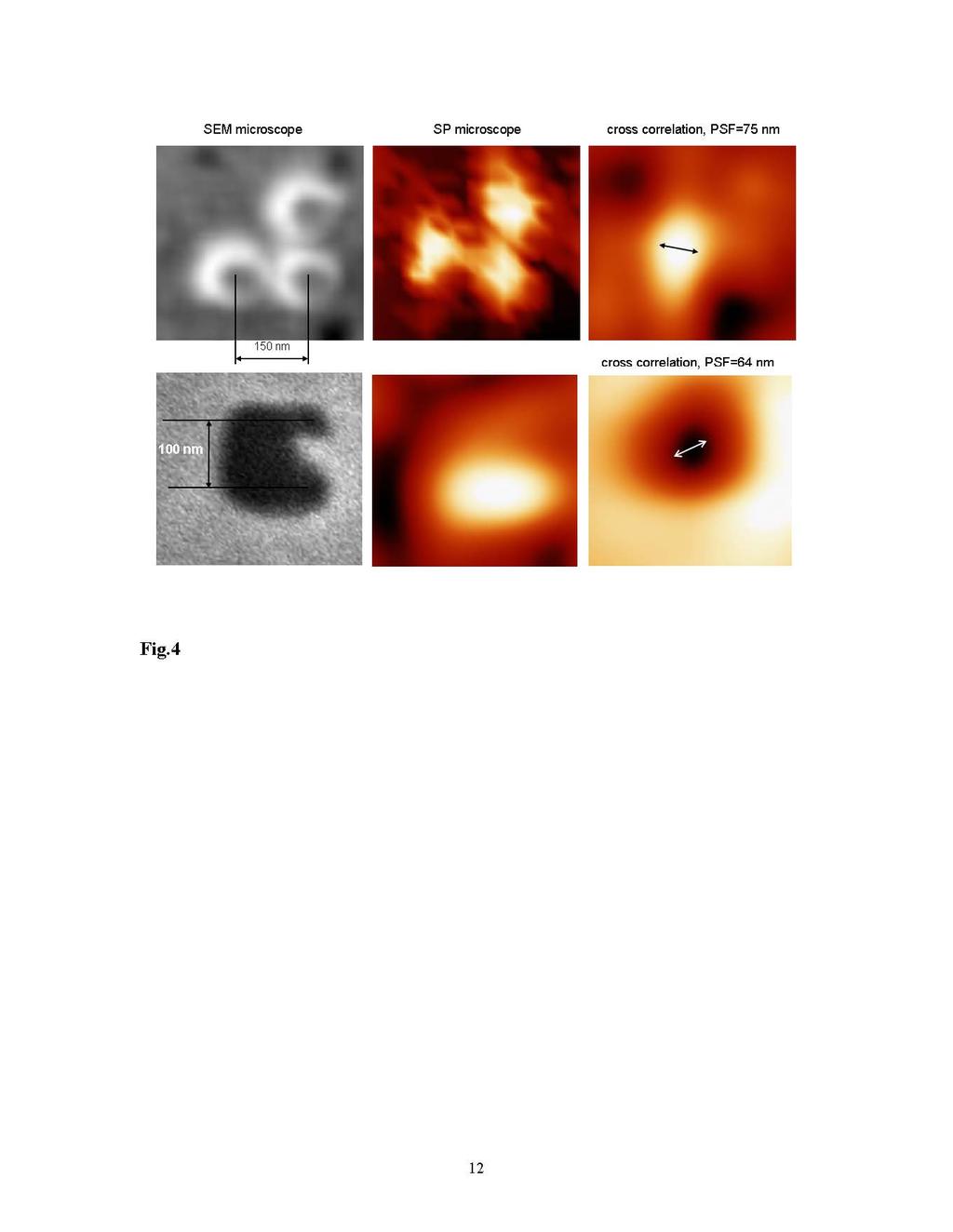
3 consisting of differently-shaped nanoholes in gold films were obtained at illuminating laser wavelengths of 502 and 515 nm, and magnified by the photonic crystal mirror and formed over the flat gold film surface (as shown in Fig.1). The resulting optical images were observed due to SPP scattering using regular optical microscope. The sign of the effective refractive index of the mirror is defined by the sign of the SPP group velocity near the surface plasmon resonance. In the experiment this sign can be determined by the character of magnification distribution in the SPP-formed images, as described in ref. [4]. Some examples of so produced optical images are shown in Figs.2 and 3. The spatial resolution of the optical images (the point spread function (PSF) of our microscope) can be measured directly by calculating the cross-correlation between the optical image and the scanning electron microscope (SEM) image of the same nanohole. The results of these calculations in the cases of triplet and U-shaped nanoholes from Figs. 2 and 3 are presented in Fig.4. These calculations demonstrate resolution of the order of PSF~70 nm or ~λ/8 achieved in these particular imaging experiments. It should be noted that similar resolution of the order of 90 nm at 413 nm laser wavelength was observed recently in focusing experiments with planar parabolic solid immersion mirrors even without the use of surface plasmon polaritons (regular guided modes were used) [6]. Slightly better resolution in our microscopy experiment is due to the fact that SPP wavelength is shorter than the wavelength of guided modes at the same laser frequency. Photonic crystal effects and the effects of negative refraction also play some role in achieving better resolution, as described in ref. [4]. Even though quite an improvement compared to a regular optical microscope, the ~ 70 nm resolution is not sufficient to achieve clear visibility of many nanoholes in the 3
4 test pattern in Fig.3, which was made in order to emulate variety of shapes of different biological samples. Even though recognizable, most nanoholes appear quite fuzzy. However, the blurring of optical images at the limits of optical device resolution is a very old problem (one may recall the well-publicized recent problem of Hubble telescope repair). One solution of this problem is also well-known. There exists a wide variety of image recovery techniques which successfully fight image blur based on the known PSF of the optical system. One of such techniques is matrix deconvolution based on the Laplacian filter (see Fig.5 for an example). Utilization of such techniques is known to improve resolution by at least a factor of two. However, precise knowledge of the PSF of the microscope in a given location in the image is absolutely essential for this technique to work, since it involves matrix convolution of the experimental image with a rapidly oscillating Laplacian filter matrix (an example of such 5x5 matrix is shown in Fig.5). In our test experiments the PSF of the microscope was measured directly in some particular location of the optical image, as is shown in Fig.4. This measured PSF was used to digitally enhance images of the neighboring nanohole arrays. Similar technique may be used to enhance resolution in the SPP-induced optical images of biological samples, which are measured using the nanohole array background, as described in ref.[4]. Not surprisingly, the use of such digital filters led to approximately two-fold improvement of resolution in the optical images formed by the photonic crystal mirror in both positive and negative effective refractive index cases. This two-fold improvement is demonstrated in Fig.6 for both the triplet and the U-shaped nanoholes shown in Figs 2-4. The point spread function measured as the cross-correlation between the digitally processed optical image and the corresponding SEM image appears to fall firmly into the 4
5 30 nm range, which represents improvement of resolution of the SPP-assisted optical microscope down to ~ λ/20 range. This result may bring about direct optical visualization of many important biological systems. In conclusion, we have demonstrated quantitatively that the use of photonic crystal mirror may improve resolution of immersion optical microscopy down to 80 nm level. In addition, utilization of well-known digital image recovery techniques allows us to further improve resolution of optical microscope down to 30 nm level. This result may be useful in various biological applications of the SPP-assisted microscope based on photonic crystal mirror. This work was supported in part by NSF grants ECS and CCF and by the EPSRC. 5
6 References [1]. J.B. Pendry, Phys.Rev.Lett. 85, 3966 (2000). [2]. D. W. Pohl and D. Courjon, Eds., Near Field Optics (Kluwer Academic Publ., Dordrecht, 1993). [3]. N. Fang, H. Lee, C. Sun, and X. Zhang, Science 308, 534 (2005). [4]. I.I. Smolyaninov, C.C. Davis, J. Elliott, G. Wurtz, and A.V. Zayats, Phys.Rev.B 72, (2005). [5]. A. V. Zayats, I. I. Smolyaninov, and A. A. Maradudin, Phys. Rep. 408, 131 (2005). [6] W.A. Challener, C. Mihalcea, C. Peng, and K. Pelhos, Optics Express 13, 7189 (2005). 6
7 Figure Captions Figure 1. Schematic view of the surface plasmon microscope (SPM) based on 2D photonic crystal mirror in the case of negative effective refractive index of the mirror as perceived by surface plasmon polaritons. Figure 2. Comparison of the SPP-produced optical (a) and the scanning electron microscope (SEM) images of the test array of triplet nanoholes. Comparison of the Fourier transforms of these images indicates spatial resolution in the optical image of at least 98 nm. This conclusion may be reached from the apparent visibility of higher harmonics of the triplet structure (indicated by the arrows) in the optical image. Figure 3. Scanning electron microscope (SEM) image of an aperiodic nanohole array test sample is shown is (b). The optical image of the test sample obtained using SPPs in the geometry from Fig.1 is shown in (a). The insets in (a) compare the images of a U- shaped nanohole obtained using SPPs and SEM. Figure 4. Calculated cross correlation functions between the SEM and optical images of a triplet nanohole from Fig.2 (top row) and U-shaped nanohole from Fig.3 (bottom row). These calculations indicate the point spread function of the optical microscope of the order of 70 nm. Figure 5. Theoretical modeling of the image recovery using Laplacian filter matrix deconvolution: Laplacian filter (shown in the inset) allows to recover image deterioration due to Gaussian blur, which is evidenced via calculation of the cross correlation of the original SEM image and the image recovered using Laplacian matrix deconvolution method. 7
8 Figure 6. Calculated cross correlation functions between the SEM and the digitallyenhanced optical images of a triplet nanohole from Fig.2 (top row) and U-shaped nanohole from Fig.3 (bottom row). Comparison of these images with Fig.4 indicates ~ two-fold improvement of the image resolution. Calculated PSF of the digitally-enhanced optical images appears to be of the order of 30 nm. 8
9
10
11
12
13
14
Surface plasmon dielectric waveguides
 Surface plasmon dielectric waveguides Igor I. Smolyaninov, Yu-Ju Hung, and Christopher C. Davis Department of Electrical and Computer Engineering, University of Maryland, College Park, MD 20742 Phone:
ECE280: Nano-Plasmonics and Its Applications. Week5. Extraordinary Optical Transmission (EOT)
") ECE280: Nano-Plasmonics and Its Applications Week5 Extraordinary Optical Transmission (EOT) Introduction Sub-wavelength apertures in metal films provide light confinement beyond the fundamental diffraction
ECE280: Nano-Plasmonics and Its Applications Week5 Extraordinary Optical Transmission (EOT) Introduction Sub-wavelength apertures in metal films provide light confinement beyond the fundamental diffraction
Hyperspectral imaging of plasmonic nanostructures with nanoscale resolution
 Hyperspectral imaging of plasmonic nanostructures with nanoscale resolution M. V. Bashevoy, 1 F. Jonsson, 1 K. F. MacDonald, 1* Y. Chen, 2 and N. I. Zheludev 1 1 Optoelectronics Research Centre, University
Wide-field extended-resolution fluorescence microscopy with standing surface plasmon resonance waves
 Wide-field extended-resolution fluorescence microscopy with standing surface plasmon resonance waves Euiheon Chung 1, 2, Yang-Hyo Kim 1, Wai Teng Tang 3, Colin J. R. Sheppard 4, and 1, 5* Peter T. C. So
Trapped Rainbow Techniques for Spectroscopy on a Chip and. Fluorescence Enhancement
 Trapped Rainbow Techniques for Spectroscopy on a Chip and Fluorescence Enhancement Vera N. Smolyaninova 1), Igor I. Smolyaninov 2), Alexander V. Kildishev 3) and Vladimir M. Shalaev 3) 1) Department of
Diffraction grating revisited: a high-resolution plasmonic dispersive element
 1 Diffraction grating revisited: a high-resolution plasmonic dispersive element V. Mikhailov 1, J. Elliott 2, G. Wurtz 2, P. Bayvel 1, A. V. Zayats 2* 1 Department of Electronic and Electrical Engineering,
Title: Localized surface plasmon resonance of metal nanodot and nanowire arrays studied by far-field and near-field optical microscopy
 Contract Number: AOARD-06-4074 Principal Investigator: Heh-Nan Lin Address: Department of Materials Science and Engineering, National Tsing Hua University, 101, Sec. 2, Kuang Fu Rd., Hsinchu 30013, Taiwan
Enhanced Light Trapping in Periodic Aluminum Nanorod Arrays as Cavity Resonator
 Enhanced Light Trapping in Periodic Aluminum Nanorod Arrays as Cavity Resonator Rosure B. Abdulrahman, Arif S. Alagoz, Tansel Karabacak Department of Applied Science, University of Arkansas at Little Rock,
SUPPLEMENTARY INFORMATION
 Measuring subwavelength spatial coherence with plasmonic interferometry Drew Morrill, Dongfang Li, and Domenico Pacifici School of Engineering, Brown University, Providence, RI 02912, United States List
Plasmonic Demultiplexer and Guiding
 Plasmonic Demultiplexer and Guiding Chenglong Zhao and Jiasen Zhang * State Key Laboratory for Mesoscopic Physics and Department of Physics, Peking University, Beijing, 100871, China Two-dimensional plasmonic
Plasmonics using Metal Nanoparticles. Tammy K. Lee and Parama Pal ECE 580 Nano-Electro-Opto-Bio
 Plasmonics using Metal Nanoparticles Tammy K. Lee and Parama Pal ECE 580 Nano-Electro-Opto-Bio April 1, 2007 Motivation Why study plasmonics? Miniaturization of optics and photonics to subwavelength scales
An Easy Introduction to Plasmonics
 An Easy Introduction to Plasmonics Wolfgang Freude Institute of Photonics and Quantum Electronics (IPQ), University of Karlsruhe, Germany Universität Karlsruhe (TH) Institut für Photonik und Quantenelektronik
Satoshi Kawata. Near-Field Optic s and Surface Plasmon Polaritons
 Satoshi Kawata Near-Field Optic s and Surface Plasmon Polaritons Near-Field Optics and the Surface Plasmon Polariton Dieter W. Pohl 1 1. Introduction 1 2. Back to the Roots 1 2.1. Rayleigh and Mie Scattering
Supplementary Figure S1. Scheme for the fabrication of Au nanohole array pattern and
 Supplementary Figure S1. Scheme for the fabrication of Au nanohole array pattern and the growth of hematite nanorods on the Au nanohole array substrate. (a) Briefly, the 500 nm sized PS monolayer was assembled
Tunable Nanoscale Plasmon Antenna for Localization and Enhancement of Optical Energy. Douglas Howe
 Tunable Nanoscale Plasmon Antenna for Localization and Enhancement of Optical Energy Douglas Howe Applied Optics Spring 2008 Table of Contents Abstract... 3 Introduction... 4 Surface Plasmons... 4 Nano
CREOL, The College of Optics & Photonics, University of Central Florida
 Metal Substrate Induced Control of Ag Nanoparticle Plasmon Resonances for Tunable SERS Substrates Pieter G. Kik 1, Amitabh Ghoshal 1, Manuel Marquez 2 and Min Hu 1 1 CREOL, The College of Optics and Photonics,
PLASMONIC STRUCTURES IN PMMA RESIST
 PLASMONIC STRUCTURES IN PMMA RESIST Michal URBÁNEK a, Stanislav KRÁTKÝ a, MARCEL ŠIMÍK b, Vladimír KOLAŘÍK a, Miroslav HORÁČEK a, Milan MATĚJKA a a Institute of Scientific Instruments of the ASCR, v.v.i.,
Direct observation of surface plasmon-polariton dispersion
 Direct observation of surface plasmon-polariton dispersion Armando Giannattasio and William L. Barnes School of Physics, University of Exeter, Stocker Road, Exeter, EX4 4QL, United Kingdom a.giannattasio@exeter.ac.uk
Optical Nano-Imaging of Metallic Nanostructures
 Optical Nano-Imaging of Metallic Nanostructures Antonello Nesci * and Olivier J. F. Martin Swiss Federal Institute of Technology Lausanne (EPFL), Nanophotonics & Metrology Laboratory EPFL-STI-NAM, station
Electric Field Distribution of Nanohole Thin Gold Film for Plasmonic Biosensor: Finite Element Method
 Electric Field Distribution of Nanohole Thin Gold Film for Plasmonic Biosensor: Finite Element Method M. Khammar Center for Development of Advanced Technologies (CDTA), Research Unit in Optics and Photonics
Using Atomic Force Microscopy (AFM) for Engineering Low Scatter Thin Film Optics
 for Engineering Low Scatter Thin Film Optics") The World Leader In Scanning Probe Microscopy Using Atomic Force Microscopy (AFM) for Engineering Low Scatter Thin Film Optics By A. Duparré, N. Kaiser, M.G. Heaton Figure 2: AFM image of the surface structures
The World Leader In Scanning Probe Microscopy Using Atomic Force Microscopy (AFM) for Engineering Low Scatter Thin Film Optics By A. Duparré, N. Kaiser, M.G. Heaton Figure 2: AFM image of the surface structures
Coupled surface plasmon polaritons on thin metal slabs corrugated on both surfaces
 PHYSICAL REVIEW B 70, 045421 (2004) Coupled surface plasmon polaritons on thin metal slabs corrugated on both surfaces I. R. Hooper and J. R. Sambles Thin Film Photonics, School of Physics, University
Sample region with fluorescent labeled molecules
 FLUORESCENCE IMAGING I. Fluorescence-imaging with diffraction limited spots The resolution in optical microscopy has been hampered by the smallest spot possible (~ λ/2) that can be achieved by conventional
Plasmonics: Application-oriented fabrication. Part 1. Introduction
 Plasmonics: Application-oriented fabrication Part 1. Introduction Victor Ovchinnikov Department of Aalto Nanofab Aalto University Espoo, Finland Alvar Aalto was a famous Finnish architect and designer
Stimulated emission of surface plasmon polaritons
 Stimulated emission of surface plasmon polaritons M. A. Noginov, G. Zhu, M. F. Mayy, B. A. Ritzo, N. Noginova, and V. A. Podolskiy ) Center for Materials Research, Norfolk State University, Norfolk, VA
SPP waveguides. Introduction Size Mismatch between Scaled CMOS Electronics and Planar Photonics. dielectric waveguide ~ 10.
 SPP waveguides Introduction Size Mismatch between Scaled CMOS Electronics and Planar Photonics CMOS transistor: Medium-sized molecule dielectric waveguide ~ 10 Silicon Photonics? Could such an Architecture
Supporting Information. Two-Photon Luminescence of Single Colloidal Gold NanoRods: Revealing the Origin of Plasmon Relaxation in Small Nanocrystals
 Supporting Information Two-Photon Luminescence of Single Colloidal Gold NanoRods: Revealing the Origin of Plasmon Relaxation in Small Nanocrystals Céline Molinaro 1, Yara El Harfouch 1, Etienne Palleau
Building An Ultrafast Photon-Induced Near-field Transmission Electron Microscope
 Building An Ultrafast Photon-Induced Near-field Transmission Electron Microscope Dr. Tom T.A. Lummen École Polytechnique Fédérale de Lausanne -- LUMES Photonic Instruments 2013 September 11, 2013 Zürich,
Chapter 3 Basic Crystallography and Electron Diffraction from Crystals. Lecture 9. Chapter 3 CHEM Fall, L. Ma
 Chapter 3 Basic Crystallography and Electron Diffraction from Crystals Lecture 9 Outline The geometry of electron diffraction Crystallography Kinetic Theory of Electron diffraction Diffraction from crystals
applications were proposed and demonstrated so far, such as medical diagnostics [1,2], security applications [3-5], drug inspection [6], etc. Especial
![applications were proposed and demonstrated so far, such as medical diagnostics [1,2], security applications [3-5], drug inspection [6], etc. Especial](/thumbs/89/100565815.jpg "applications were proposed and demonstrated so far, such as medical diagnostics [1,2], security applications [3-5], drug inspection [6], etc. Especial") Highly sensitive surface plasmon terahertz imaging with planar plasmonic crystals F. Miyamaru 1, 2 *, M. W. Takeda 1, T. Suzuki 2 and C. Otani 2 1 Department of Physics, Shinshu University, 3-1-1 Asahi,
Highly sensitive surface plasmon terahertz imaging with planar plasmonic crystals F. Miyamaru 1, 2 *, M. W. Takeda 1, T. Suzuki 2 and C. Otani 2 1 Department of Physics, Shinshu University, 3-1-1 Asahi,
Surface plasmon polaritons on narrow-ridged short-pitch metal gratings in the conical mount
 836 J. Opt. Soc. Am. A/ Vol. 20, No. 5/ May 2003 I. R. Hooper and J. R. Sambles Surface plasmon polaritons on narrow-ridged short-pitch metal gratings in the conical mount Ian R. Hooper and J. R. Sambles
Nanostructured Plasmonic Interferometers for Ultrasensitive Label-Free Biosensing. Fil Bartoli Lehigh University 4/9/2014
 Nanostructured Plasmonic Interferometers for Ultrasensitive Label-Free Biosensing Fil Bartoli Lehigh University 4/9/2014 P.C. Rossin College of Engineering and Applied Science Department of Electrical
Reviewers' comments: Reviewer #1 (Remarks to the Author):
:") Reviewers' comments: Reviewer #1 (Remarks to the Author): In their manuscript "Single Molecule Mirage: shifted molecular localizations through plasmonic coupling", Raab et al evaluate the effect that plasmonic
Reviewers' comments: Reviewer #1 (Remarks to the Author): In their manuscript "Single Molecule Mirage: shifted molecular localizations through plasmonic coupling", Raab et al evaluate the effect that plasmonic
Directional Surface Plasmon Coupled Emission
 Journal of Fluorescence, Vol. 14, No. 1, January 2004 ( 2004) Fluorescence News Directional Surface Plasmon Coupled Emission KEY WORDS: Surface plasmon coupled emission; high sensitivity detection; reduced
arxiv: v1 [physics.optics] 3 Feb 2010
![arxiv: v1 [physics.optics] 3 Feb 2010](/thumbs/72/66601340.jpg "arxiv: v1 [physics.optics] 3 Feb 2010") Plasmonic crystal demultiplexer and multiports Aurelien Drezet, Daniel Koller, Andreas Hohenau, Alfred Leitner, Franz R. Aussenegg, and Joachim R. Krenn Institute of Physics and Erwin Schrödinger Institute
Plasmonic crystal demultiplexer and multiports Aurelien Drezet, Daniel Koller, Andreas Hohenau, Alfred Leitner, Franz R. Aussenegg, and Joachim R. Krenn Institute of Physics and Erwin Schrödinger Institute
Special Techniques 1. Mark Scott FILM Facility
 Special Techniques 1 Mark Scott FILM Facility SPECIAL TECHNIQUES Multi-photon microscopy Second Harmonic Generation FRAP FRET FLIM In-vivo imaging TWO-PHOTON MICROSCOPY Alternative to confocal and deconvolution
Plasmonic Nanostructures II
 Plasmonic Nanostructures II Dr. Krüger / Prof. M. Zacharias, IMTEK, Propagation of SPPs Propagation distance decreases with decreasing strip width! 2 Dr. Krüger / Prof. M. Zacharias, IMTEK, Bound and leaky
Enhanced and suppressed transmission through metal gratings at the plasmonic band edges
 Enhanced and suppressed transmission through metal gratings at the plasmonic band edges M. J. Bloemer, D. de Ceglia*, M. A. Vincenti*, M. Scalora, N. Akozbek Charles M. Bowden Laboratory, AMSRD-AMR-WS,
Fabrication of photonic band-gap crystals
 Fabrication of photonic band-gap crystals C. C. Cheng and A. Scherer California Institute of Technology, Pasadena, California 91125 Received 19 June 1995; accepted 9 August 1995 We describe the fabrication
Confocal Microscopy & Imaging Technology. Yan Wu
 Confocal Microscopy & Imaging Technology Yan Wu Dec. 05, 2014 Cells under the microscope What we use to see the details of the cell? Light and Electron Microscopy - Bright light / fluorescence microscopy
Efficient directional beaming from small apertures using surface-plasmon diffraction gratings
 Efficient directional beaming from small apertures using surface-plasmon diffraction gratings Youngkyu Lee, Kazunori Hoshino, Andrea Alù, and Xiaojing Zhang Citation: Applied Physics Letters 101, 041102
SUPPLEMENTARY INFORMATION. Efficient unidirectional polarization-controlled excitation of. surface plasmon polaritons
 SUPPLEMENTARY INFORMATION Efficient unidirectional polarization-controlled excitation of surface plasmon polaritons Anders Pors 1,*, Michael G. Nielsen 1,2,*, Thomas Bernardin 2, Jean-Claude Weeber 2 &
Light Trapping Enhancement in Thin Film Silicon Solar Cell with Different Back Reflector
 International Journal of Electrical Components and Energy Conversion 2017; 3(5): 83-87 http://www.sciencepublishinggroup.com/j/ijecec doi: 10.11648/j.ijecec.20170305.11 ISSN: 2469-8040 (Print); ISSN: 2469-8059
Compact hybrid plasmonic-si waveguide structures utilizing Albanova E-beam lithography system
 Compact hybrid plasmonic-si waveguide structures utilizing Albanova E-beam lithography system Introduction Xu Sun Laboratory of Photonics and Microwave Engineering, Royal Institute of Technology (KTH),
micromachines ISSN X
 Micromachines 2012, 3, 55-61; doi:10.3390/mi3010055 Article OPEN ACCESS micromachines ISSN 2072-666X www.mdpi.com/journal/micromachines Surface Plasmon Excitation and Localization by Metal-Coated Axicon
Cell analysis and bioimaging technology illustrated
 Cell analysis and bioimaging technology illustrated The Cell Analysis Center Scientific Bulletin Part 1 Sysmex has been studying and exploring principles of automated haematology analysers, making full
Symposium 20 years of nano-optics April 6th, 2004 Auditorium, Institute of Physics, St.Johanns-Ring 25
 Symposium 20 years of nano-optics April 6th, 2004 Auditorium, Institute of Physics, St.Johanns-Ring 25 9:30 9:45 Coffee and Gipfeli 9:45 10:00 Welcome address and introduction B. Hecht Uni Basel H.-J.
Single crystal X-ray diffraction. Zsolt Kovács
 Single crystal X-ray diffraction Zsolt Kovács based on the Hungarian version of the Laue lab description which was written by Levente Balogh, Jenő Gubicza and Lehel Zsoldos INTRODUCTION X-ray diffraction
Integrated Heat Assisted Magnetic Recording Head: Design & Recording Demonstration
 > FOR CONFERENCE-RELATED PAPERS, REPLACE THIS LINE WITH YOUR SESSION NUMBER, E.G., AB-2 (DOUBLE-CLICK HERE) < 1 Integrated Heat Assisted Magnetic Recording Head: Design & Recording Demonstration Michael
Mater. Res. Soc. Symp. Proc. Vol Materials Research Society
 Mater. Res. Soc. Symp. Proc. Vol. 940 2006 Materials Research Society 0940-P13-12 A Novel Fabrication Technique for Developing Metal Nanodroplet Arrays Christopher Edgar, Chad Johns, and M. Saif Islam
Fundamentals of X-ray diffraction and scattering
 Fundamentals of X-ray diffraction and scattering Don Savage dsavage@wisc.edu 1231 Engineering Research Building (608) 263-0831 X-ray diffraction and X-ray scattering Involves the elastic scattering of
Supplementary Figure 1 Scanning electron micrograph (SEM) of a groove-structured silicon substrate. The micropillars are ca. 10 μm wide, 20 μm high
 of a groove-structured silicon substrate. The micropillars are ca. 10 μm wide, 20 μm high") Supplementary Figure 1 Scanning electron micrograph (SEM) of a groove-structured silicon substrate. The micropillars are ca. 10 μm wide, 20 μm high and own the gap of 10 μm. Supplementary Figure 2 Strictly
Supplementary Figure 1 Scanning electron micrograph (SEM) of a groove-structured silicon substrate. The micropillars are ca. 10 μm wide, 20 μm high and own the gap of 10 μm. Supplementary Figure 2 Strictly
Seminar: Structural characterization of photonic crystals based on synthetic and natural opals. Olga Kavtreva. July 19, 2005
 Seminar: Structural characterization of photonic crystals based on synthetic and natural opals Olga Kavtreva July 19, 2005 Abstract Novel class of dielectric structures with a refractive index which exhibits
Dispersion characteristics of silicon nanorod based carpet cloaks
 Dispersion characteristics of silicon nanorod based carpet cloaks Venkata A. Tamma 1, John Blair 2, Christopher J. Summers 2 and Wounjhang Park 1* 1 Department of Electrical, Computer & Energy Engineering,
Optical microscopy Theoretical background Galina Kubyshkina
 Optical microscopy Theoretical background Galina Kubyshkina Elektromaterial Lendava d.d., Slovenia Crystalline materials presence of a unit (cell), which is periodically repeated in space regular structure
Supplementary Information
 Supplementary Information Trapping and Detection of Nanoparticles and Cells Using a Parallel Photonic Nanojet Array Yuchao Li, Hongbao Xin, Xiaoshuai Liu, Yao Zhang, Hongxiang Lei*, and Baojun Li* State
The actual laser manufacturing process seem to be quite straightforward and reproducible by a third party researcher.
 Reviewers' comments: Reviewer #1 (Remarks to the Author): The authors have used ps laser to make nanoparticles on silver surface so that different visible colors can be realized due to the light absorption
Microscopy. CS/CME/BioE/Biophys/BMI 279 Nov. 2, 2017 Ron Dror
 Microscopy CS/CME/BioE/Biophys/BMI 279 Nov. 2, 2017 Ron Dror 1 Outline Microscopy: the basics Fluorescence microscopy Resolution limits The diffraction limit Beating the diffraction limit 2 Microscopy:
Active delivery of single DNA molecules into a plasmonic nanopore for. label-free optical sensing
 Supporting Information: Active delivery of single DNA molecules into a plasmonic nanopore for label-free optical sensing Xin Shi 1,2, Daniel V Verschueren 1, and Cees Dekker 1* 1. Department of Bionanoscience,
Crystallographic Characterization of GaN Nanowires by Raman Spectral Image Mapping
 Crystallographic Characterization of GaN Nanowires by Raman Spectral Image Mapping Heerad Farkhoor, Adam Schwartzberg, Jeffrey Urban August 12, 2009 Abstract Obtaining structural information of nano-structured
Modeling Of A Diffraction Grating Coupled Waveguide Based Biosensor For Microfluidic Applications Yixuan Wu* 1, Mark L. Adams 1 1
 Modeling Of A Diffraction Grating Coupled Waveguide Based Biosensor For Microfluidic Applications Yixuan Wu* 1, Mark L. Adams 1 1 Auburn University *yzw0040@auburn.edu Abstract: A diffraction grating coupled
Low-cost, deterministic quasi-periodic photonic structures for light trapping in thin film silicon solar cells
 Low-cost, deterministic quasi-periodic photonic structures for light trapping in thin film silicon solar cells The MIT Faculty has made this article openly available. Please share how this access benefits
Surface plasmon enhanced emission from dye doped polymer layers
 Surface plasmon enhanced emission from dye doped polymer layers Terrell D. Neal, a) Koichi Okamoto, and Axel Scherer Department of Electrical Engineering, California Institute of Technology, Pasadena,
Research Projects in Nano-Technology
 Research Projects in Nano-Technology Ibrahim Abdulhalim Our research is multidisciplinary combining nanostructures, liquid crystals, devices and methods for biosensing and biomedical optical imaging applications.
White Paper: Pixelligent Internal Light Extraction Layer for OLED Lighting
 White Paper: Pixelligent Internal Light Zhiyun (Gene) Chen, Ph.D., Vice President of Engineering Jian Wang, Ph.D., Manager, Application Engineering Pixelligent Technologies LLC, 6411 Beckley Street, Baltimore,
Lecture 13 Nanophotonics in plasmonics. EECS Winter 2006 Nanophotonics and Nano-scale Fabrication P.C.Ku
 Lecture 13 Nanophotonics in plasmonics EECS 598-002 Winter 2006 Nanophotonics and Nano-scale Fabrication P.C.Ku Schedule for the rest of the semester Introduction to light-matter interaction (1/26): How
Silver Diffusion Bonding and Layer Transfer of Lithium Niobate to Silicon
 Chapter 5 Silver Diffusion Bonding and Layer Transfer of Lithium Niobate to Silicon 5.1 Introduction In this chapter, we discuss a method of metallic bonding between two deposited silver layers. A diffusion
THIN METALLIC LAYERS STRUCTURED BY E-BEAM LITHOGRAPHY. Miroslav HORÁČEK, Vladimír KOLAŘÍK, Michal URBÁNEK, František MATĚJKA, Milan MATĚJKA
 THIN METALLIC LAYERS STRUCTURED BY E-BEAM LITHOGRAPHY Miroslav HORÁČEK, Vladimír KOLAŘÍK, Michal URBÁNEK, František MATĚJKA, Milan MATĚJKA Ústav přístrojové techniky AV ČR, v. v. i., Královopolská 147,
Confocal Microscopy of Electronic Devices. James Saczuk. Consumer Optical Electronics EE594 02/22/2000
 Confocal Microscopy of Electronic Devices James Saczuk Consumer Optical Electronics EE594 02/22/2000 Introduction! Review of confocal principles! Why is CM used to examine electronics?! Several methods
Surface Plasmon Effects in Nano-Optics. Greg Gbur Department of Physics and Optical Science, UNC Charlotte, Charlotte, North Carolina 28227
 Surface Plasmon Effects in Nano-Optics Greg Gbur Department of Physics and Optical Science, UNC Charlotte, Charlotte, North Carolina 28227 Shanghai, Jan 2007 Summary Introduction: What is a surface plasmon?
EUV Transmission Lens Design and Manufacturing Method
 1 EUV Transmission Lens Design and Manufacturing Method Kenneth C. Johnson kjinnovation@earthlink.net 7/9/2018 Abstract This paper outlines a design for an EUV transmission lens comprising blazed, phase-
Plasmonic Luneburg and Eaton Lenses
 Plasmonic Luneburg and Eaton Lenses Thomas Zentgraf 1*, Yongmin Liu 1*, Maiken H. Mikkelsen 1*, Jason Valentine 1,3, Xiang Zhang 1,2, 1 NSF Nanoscale Science and Engineering Center (NSEC), 3112 Etcheverry
Verification of thickness and surface roughness of a thin film transparent coating
 Verification of thickness and surface roughness of a thin film transparent coating K. Mohaghegh 1, H.N. Hansen 1, H. Pranov 2, G. Kofod 2 1 Technical University of Denmark, Denmark 2 InMold Biosystems,
Thin Film Micro-Optics
 Thin Film Micro-Optics New Frontiers of Spatio-Temporal Beam Shaping Ruediger Grunwald Max Born Institut for Nonlinear Optics and Short Pulse Spectroscopy Berlin, Germany ELSEVIER Amsterdam Boston Heidelberg
Efficient directional excitation of surface plasmons by a singleelement nanoantenna (Supporting Information)
") Efficient directional excitation of surface plasmons by a singleelement nanoantenna (Supporting Information) Wenjie Yao, #, Shang Liu, #, Huimin Liao, *, Zhi Li, *, Chengwei Sun,, Jianjun Chen,, and Qihuang
Efficient directional excitation of surface plasmons by a singleelement nanoantenna (Supporting Information) Wenjie Yao, #, Shang Liu, #, Huimin Liao, *, Zhi Li, *, Chengwei Sun,, Jianjun Chen,, and Qihuang
Effect of Substrate Discontinuities on the Propagating Surface Plasmon Polariton
 Electronic Supplementary Material (ESI) for Nanoscale. This journal is The Royal Society of Chemistry 2014 Supplemental Information for: Effect of Substrate Discontinuities on the Propagating Surface Plasmon
IMMERSION HOLOGRAPHIC RECORDING OF SUBWAVELENGTH GRATINGS IN AMORPHOUS CHALCOGENIDE THIN FILMS
 Journal of Optoelectronics and Advanced Materials Vol. 7, No. 5, October 2005, p. 2581-2586 IMMERSION HOLOGRAPHIC RECORDING OF SUBWAVELENGTH GRATINGS IN AMORPHOUS CHALCOGENIDE THIN FILMS J. Teteris *,
Rayleigh anomaly-surface plasmon polariton resonances in palladium and gold subwavelength hole arrays
 Rayleigh anomaly-surface plasmon polariton resonances in palladium and gold subwavelength hole arrays H. Gao, 1 J. M. McMahon, 2, 3 M. H. Lee, 2 J. Henzie, 2 S. K. Gray, 3 G. C. Schatz, 2 1, 2* and T.
Interferometric optical biosensor. Xingwei Wang
 Interferometric optical biosensor Xingwei Wang 1 Light Transverse electromagnetic wave Reflection Refraction Diffraction Interference 2 Fabry-Perot interferometer 3 Interferometer Two waves that coincide
Supplementary Information
 Supplementary Information Facile growth of hierarchical hematite ( -Fe 2 O 3 ) nanopetals on FTO by pulse reverse electrodeposition for photoelectrochemical water splitting Pravin S. Shinde, Geun Ho Go
Introduction to Lithography
 Introduction to Lithography G. D. Hutcheson, et al., Scientific American, 290, 76 (2004). Moore s Law Intel Co-Founder Gordon E. Moore Cramming More Components Onto Integrated Circuits Author: Gordon E.
Engineering in the Optimization of Resolution of Nanohole Arrays in Metal Films for Refractive Index Sensing
 Engineering in the Optimization of Resolution of Nanohole Arrays in Metal Films for Refractive Index Sensing by Gabriela Andrea Cervantes Téllez B.Sc., Instituto Tecnológico de Estudios Superiores de Monterrey,
ATOMIC LAYER DEPOSITION FOR PHOTONIC CRYSTAL DEVICES
 ATOMIC LAYER DEPOSITION FOR PHOTONIC CRYSTAL DEVICES E. Graugnard, J. S. King, D. Heineman, and C. J. Summers School of Materials Science and Engineering, Georgia Institute of Technology, Atlanta, GA,
Optical Biosensing Technology based on Surface Plasmon Resonance
 Department of Electronic Engineering Optical Biosensing Technology based on Surface Plasmon Resonance Aaron H.P. Ho CIOEC 2011, 7-8 September 2011 Outline of Presentation!! Introduction: Plasmonics and
Efficiency of local surface plasmon polariton excitation on ridges
 Efficiency of local surface plasmon polariton excitation on ridges I. P. Radko, 1, * S. I. Bozhevolnyi, 2, G. Brucoli, 3 L. Martín-Moreno, 3 F. J. García-Vidal, 4 and A. Boltasseva 5 1 Department of Physics
Tuning the transmission of surface plasmon polaritons across nano and micro gaps in gold stripes
 Erschienen in: Optics Express ; 24 (2016), 15. - S. 17313-17320 https://dx.doi.org/10.1364/oe.24.017313 Tuning the transmission of surface plasmon polaritons across nano and micro gaps in gold stripes
Efficient excitation of dielectric-loaded surface plasmon-polariton waveguide modes at telecommunication wavelengths
 Efficient excitation of dielectric-loaded surface plasmon-polariton waveguide modes at telecommunication wavelengths Holmgaard, T., Bozhevolnyi, S. I., Markey, L., Dereux, A., Krasavin, A. V., Bolger,
How grooves reflect and confine surface plasmon polaritons
 How grooves reflect and confine surface plasmon polaritons Martin Kuttge, 1,* F. Javier García de Abajo, 2 and Albert Polman 1 1 Center for Nanophotonics, FOM-Institute AMOLF, Sciencepark 113, 1098 XG
Supplementary material 1: DNA tracing
 Supplementary material 1: DNA tracing Figure S1:Typical AFM image showing DNA molecules relaxed when deposited with Mg 2+ DNA molecules that appear to have a higher or larger end (indicated by a red arrow
Supporting Information
 Digital Microarrays: Single-Molecule Readout with Interferometric Detection of Plasmonic Nanorod Labels Derin Sevenler 1, George G. Daaboul 2, Fulya Ekiz Kanik 1, Neşe Lortlar Ünlü 3 and M. Selim Ünlü
Foundations in Microbiology Seventh Edition
 Lecture PowerPoint to accompany Foundations in Microbiology Seventh Edition Talaro Chapter 3 Tools of the Laboratory: The Methods for Studying Microorganisms Copyright The McGraw-Hill Companies, Inc. Permission
Enhancement Surface Mechanical Properties of 2024 Al-Alloys Using Pulsed Nd:YAG Laser Cladding
 Enhancement Surface Mechanical Properties of 2024 Al-Alloys Using Pulsed Nd:YAG Laser Cladding 1 1 2 Raid M.HadiP P, Mahmoad Sh. MahmoadP P and Ali H.AbdalhadiP Institute of laser for postgraduate studies,
7-2E. Photonic crystals
 7-2E. Photonic crystals Purdue Univ, Prof. Shalaev, http://cobweb.ecn.purdue.edu/~shalaev/ Univ Central Florida, CREOL, Prof Kik, http://sharepoint.optics.ucf.edu/kik/ose6938i/handouts/forms/allitems.aspx
Performance and characterisation of CsI:Tl thin films for X ray imaging application
 Performance and characterisation of CsI:Tl thin films for X ray imaging application E. A. Kozyrev, K. E. Kuper, A. G. Lemzyakov, A. V. Petrozhitskiy, and A. S. Popov Budker Institute of Nuclear Physics
Evaluation of Failure in Low-k Films Using Stiffness Mapping and Dynamic Imaging
 Evaluation of Failure in Low-k Films Using Stiffness Mapping and Dynamic Imaging Application Note Introduction Fracture toughness and scratch failure of thin films on the nano-scale is of particular interest
Photonic Crystals Quantum Cascade Lasers in THz regime
 Photonic Crystals Quantum Cascade Lasers in THz regime Speaker: Roland Cerna EPFL Doctoral course 2009 Photonic Crystals Lecturer: Dr. Romuald Houdé Outline Motivation Introduction Quantum cascade laser
NANOPHOTONICS. Surface Plasmonic Fields in
 Kevin Tetz The fi eld of nanophotonics is fi nding myriad applications in information technology, health care, lighting, sensing and national security. This article explores the ultrafast electrodynamics
Supplementary Information: Hybrid polymer photonic crystal fiber with integrated chalcogenide. glass nanofilms
 Supplementary Information: Hybrid polymer photonic crystal fiber with integrated chalcogenide glass nanofilms Christos Markos, Irnis Kubat, and Ole Bang DTU Fotonik, Department of Photonics Engineering,
Micron-Resolution Photocurrent of CdTe Solar Cells Using Multiple Wavelengths
 Mat. Res. Soc. Symp. Proc. Vol. 668 2001 Materials Research Society Micron-Resolution Photocurrent of CdTe Solar Cells Using Multiple Wavelengths Jason F. Hiltner 1 and James R. Sites Department of Physics,
Pavel Kwiecien publication list
 Journal Articles Pavel Kwiecien publication list B. Špačková, P. Lebrušková, H. Šípová, P. Kwiecien, I. Richter, J. Homola, Ambiguous refractive index sensitivity of Fano resonance on an array of gold