SPP waveguides. Introduction Size Mismatch between Scaled CMOS Electronics and Planar Photonics. dielectric waveguide ~ 10.
|
|
|
- Mariah Sandra Hart
- 5 years ago
- Views:
Transcription
1 SPP waveguides Introduction Size Mismatch between Scaled CMOS Electronics and Planar Photonics CMOS transistor: Medium-sized molecule dielectric waveguide ~ 10

2 Silicon Photonics?

3 Could such an Architecture be Realized with Metal rather than Dielectric Waveguide Technology?

4 Metal Optics: An introduction Photonic functionality based on metals?!

5 Harry Atwater, California Institute of Technology A World of Nanophotonic Devices On-chip light source Long-range(~ cm) waveguides ~ cm Short-range(~ nm) waveguides Photonic integrated circuit Nano-photonics Nano-electronics Could such an Architecture be Realized with Metal rather than Dielectric Waveguide Technology?
6 Plasmons at Planar Metal-Dielectric Interfaces surface plasmons are longitudinal charge density fluctuations on the surface of a conductor surface plasmon dispersion relation: k x : dielectric : metal c x (10 15 s -1 ) Surface Plasmon dispersion relation for Ag in air Harry Atwater, California Institute of Technology = 337 nm =c k x (Light line) =337 nm; 1 = -1 Plasmon Dispersion Relation k x ( m -1 ) << 337 nm Plasmons are highly localized at metal-dielectric interfaces, so potential for: Ultrasmall Optical Devices 2D-Optics on metal surfaces
7 Nano Focusing & Wave Guiding 8 =c k x ' 1 At large kx ( 1 2), z i. kx E ie ( air : i, metal :- i) z x 6 =337 nm; 1 = -1 Strong confinement at the interface (10 15 s -1 ) 4 2 Broad dispersion Nano focusing k x ( m -1 ) At low k ( 1), E E z x x i ' 1 ' 1 in air : E E z x i 1 ' 1 in metal : Low loss at the interface Wave guiding

 total (fiber-to-fiber) insertion loss of approx.")
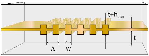
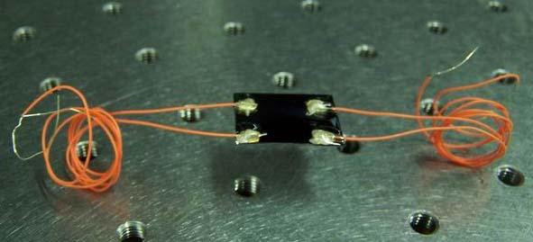
8 Several 1 cm long, 15 nm thin and 8 micron wide gold stripes guiding LRSPPs 3-6 mm long control electrodes low driving powers (approx. 100 mw) and high extinction ratios (approx. 30 db) response times (approx. 0.5 ms) total (fiber-to-fiber) insertion loss of approx. 8 db when using single-mode fibers
9

10


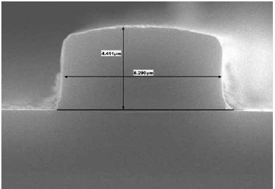
11 Fundamental symmetric mode of a metal stripe : thickness (T) W=10um T LR-SP WG 14nm 16nm 18nm 20nm
12 P. Berini, PhotonicWest 2005.
13 (Spectalis Co.)


14 Fundamental asymmetric mode of a metal stripe : n n T=16 nm, W=10um n = n = n = 0.003

 9 m 20nm")
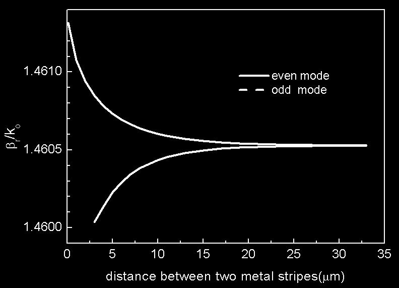
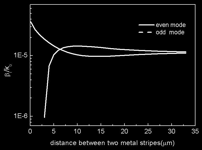
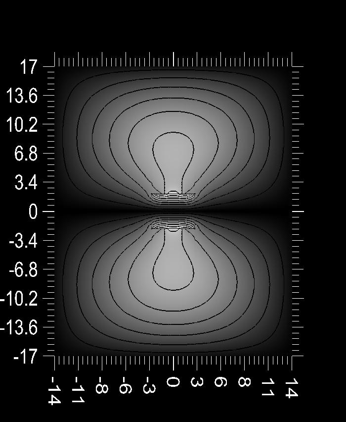
15 Symmetric mode guided by a metallic channel waveguide fiber Polymer 1.55 m silicon Au (-96+i11) 9 m 20nm 15mm ~10 m Propagation loss : 21dB/ cm


16 Y-branch Channel-1 Channel-2 1 2
17
18
19
20
21 Wavelength shifts by direct heating a metal wire Polymer 2 INPUT OUTPUT + - Polymer 1 Substrate Transmittance (db) Wavelength (nm)


22 Tunable Wavelength Filter
")
23 Vertical directional couplers H. Won, APL vol.88, (2006)


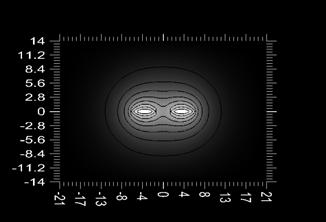
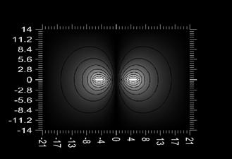
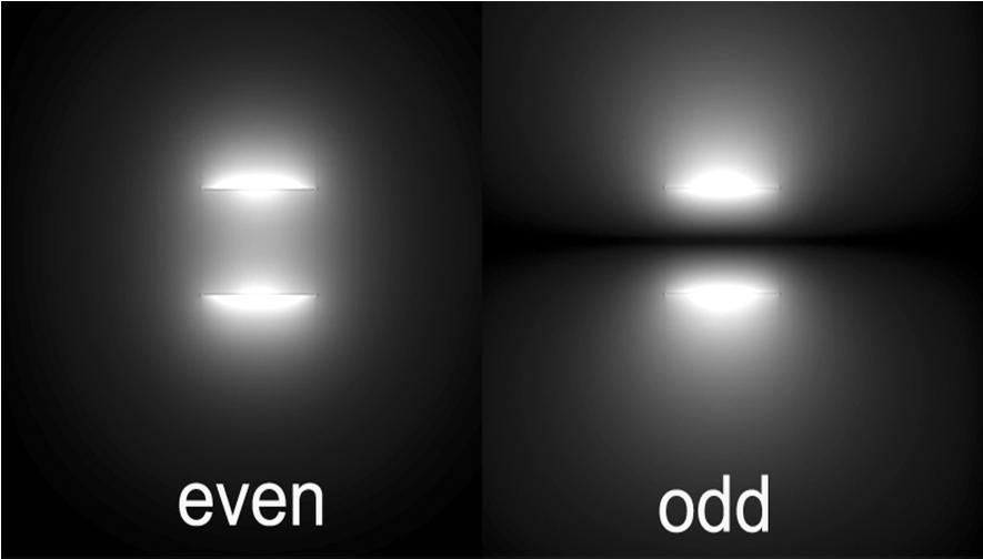
24 Vertical directional couplers d=4um 254 um d=6um 558 um m i t= 20nm d d R /k metal = i (gold) dielectric = =1550nm t=20nm symmetric even mode symmetric odd mode distance(d : distance between two slabs)


25 Even mode and odd mode : directional couplers based on LRSPP Vertical D Lateral D m, even mode m, odd mode m, even mode m, odd mode m, even mode m, odd mode m, even mode m, odd mode m, even mode m, odd mode m, even mode m, odd mode
26 Vertical directional couplers odd odd even mode odd mode Lateral DC

27 Vertical directional couplers Channel 1 Channel 2 Extinction ration at 400um : 27dB
28 Variable optical attenuator based on LR-SPP Submitted to EL, S. Park & S. Song
29 Extremely long-range SPP? Symmetrically coupled LRSP frequency Anti-symmetrically coupled LRSP in-plane wavevector

 P.")

 n4 metal n3")
30 Extension of SPP propagation length LR SPP Thin metal film Finite-width metal strip D. Sarid (PRL, 1981) J. J. Burke (APL, 1986) P. Berini (PRB, 2000) Double metal films n2 > n1 Metal-dielectric films n1 > n0~n4 Metal n1 n2 n1 G. I. Stegman et al (APL, 1983) n4 metal n3 n2 n1 n0 F. Y. Kou et al (OL, 1987)


 10 1 0.")

31 Extended Long-Range SPPs n1 Metal n2 n D n5 ~n1> n0~n2~n4 n5 n4 metal n3 n2 n1 n0 propagation length(mm) separation distance(d : m)


32 Range extension with finite-width metal stripes t n 1 n 2 D No good w Two fundamental modes Even mode only D<D cutoff n 2 < n 1
 n 2 1.40 1.45 1.46 Cutoff (D: m ) 0.23 0.78 1.78 P-length (mm) 240 230 60 Propagation length of a single stripe is only about 11mm.")
33 propagation length (mm) Propagation length and effective index separation distance (D: m) n w 5 m t 20nm m i, nm r /k separation distance (D: m) n Cutoff (D: m ) P-length (mm) Propagation length of a single stripe is only about 11mm. Propagation length of double stripes can be extended more than 10 times!

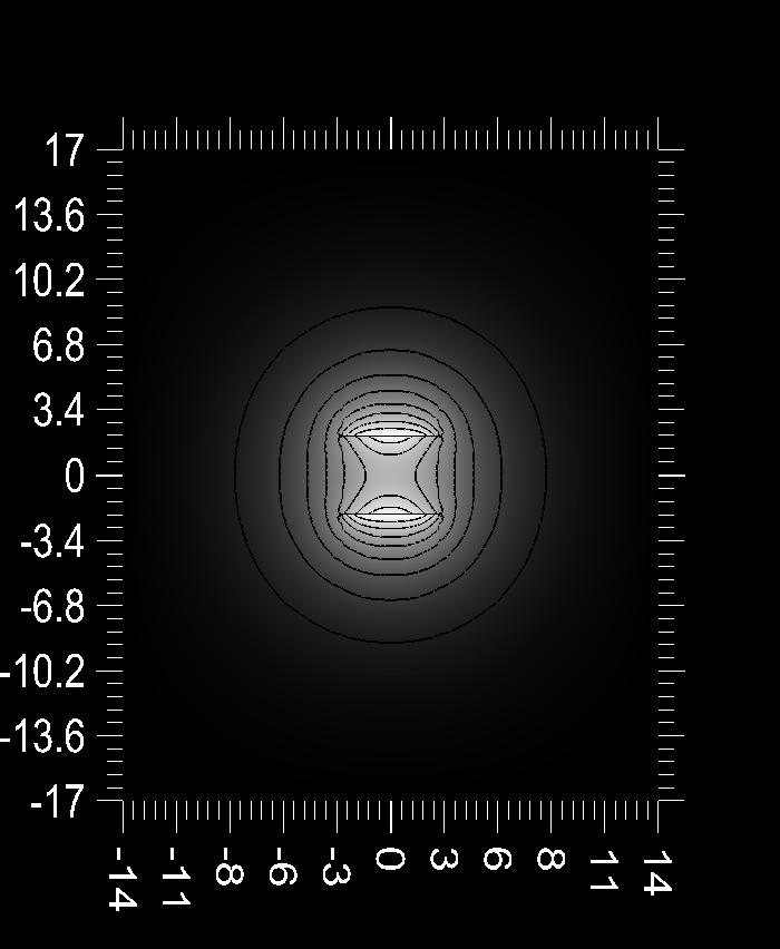
34 Mode profile & Mode size n 1.47, n 1.45, w 5 m 1 2 Double metal stripe Single metal stripe D=100nm, t= 20nm D=300nm, t= 20nm t= 20nm 10 m D=500nm, t= 20nm D=780nm, t= 20nm t= 16 nm Both of two modes have mode size of ~ 10 m Propagation length = 230 mm Propagation length = 46 mm
 0.6 0.4 metal stripe 0.2 0.")


 10 9 8 7 6 5 4 3 2 0 100 200 300 400 500")
35 Fraction of field energy in metal and area n D = 780nm 0.8 Abs(Ey) metal stripe vertical distance( m) In metal stripes In n2 dielectric fraction of the field confined metal area (%) 4.0x x x separation distance ( D : nm ) fraction of the field confined n 2 area (%) separation distance ( D : nm )
36 Butt-coupling efficiency with a SM fiber 0.70 Abs(E y ) Vertical profile double stripe single stripe coupling loss wtih fiber ( db ) Single metal strip vertical distance ( m ) thickness of metal ( t : nm) Abs(E y ) Lateral profile lateral distance ( m ) single stripe double stripe 1 double stripe 2 coupling loss wtih fiber ( db ) Double metal strips separation distance ( D : nm ) Mode profile Coupling loss with fiber
, 40 Gbit/s light")


 4 3 2 = 1310 nm 1 0 0.5 1.0 1.5 2.")

37 Plasmonic Flexible-wires for 40 GHz interconnections Jung (ETRI), 40 Gbit/s light signal transmission on a long-range SPP waveguide, APL, PTL, Tx Drive IC TIA & Pre amp IC LR-SPP waveguide SMA VCSEL array PD array SMA Rx 14 nm-thick, 2.5 m-wide gold stripes Gb/s World best Loss (db) = 1310 nm Waveguide length (cm) 0.6 db/cm : World best record in propagation loss. (Previous world record : 3.2 db/cm by Berini, 2006)


38 Double-electrode metal waveguides : Lines, S-band, Y-branch Joo, Long-range surface -plasmon--polaritons on asymmetric double-electrode structures, APL, D metal strip SPP mode d3 w 2 d1 D core metal slab d3 cladding S-band metal strip metal slab Y-branch
39 Localized Surface Plasmons : Nanofocusing and Nanolithography 8 =c k x ' 1 At large kx ( 1 2), z i. kx E ie ( air : i, metal :- i) z x 6 =337 nm; 1 = -1 Strong confinement at the interface (10 15 s -1 ) 4 2 Broad dispersion Nano focusing k x ( m -1 )
40
41 Propose metal nanowires. Propagation Loss (asymmetric mode) High Beam radius -> zero!


] 50nm * See MOVIES :")
42 Asymmetric mode : field enhancement at a metallic tip E r E r E z E z M. I. Stockman, Nanofocusing of Optical Energy in Tapered Plasmonic Waveguides, Phys. Rev. Lett. 93, (2004)] 50nm * See MOVIES : SPP propagation through a metallic tip


43 Plasmonic Crystal Demultiplexer and Multiports the realization of two-dimensional optical wavelength demultiplexers and multiports for surface plasmons polaritons (SPPs) based on plasmonic crystals, i.e., photonic crystals for SPPs.
44


45 2007/5/1 ~ an optical range resonator based on single mode metal-insulator-metal plasmonic gap waveguides. A small bridge between the resonator and the input waveguide can be used to tune the resonance frequency. FDTD with the perfectly matched layer boundary conditions


46 Slow Propagation, Anomalous Absorption, and Total External Reflection of Surface Plasmon Polaritons in Nanolayer Systems n=2 n=1 n=0

47


48 we show how the dispersion relation of surface plasmon polaritons (SPPs) propagating along a perfectly conducting wire can be tailored by corrugating its surface with a periodic array of radial grooves. Importantly, the propagation characteristics of these spoof SPPs can be controlled by the surface geometry, opening the way to important applications such as energy concentration on cylindrical wires and superfocusing using conical structures.
 : Low loss is achievable!")
49 * Short-range (asymmetric modes) : Nano localization is achievable! * Long-range (symmetric modes) : Low loss is achievable! -> Trade-off between Localization and Loss
ADOPT Winter School Merging silicon photonics and plasmonics
 ADOPT Winter School 2014 Merging silicon photonics and plasmonics Prof. Min Qiu Optics and Photonics, Royal Institute of Technology, Sweden and Optical Engineering, Zhejiang University, China Contents
Plasmonics using Metal Nanoparticles. Tammy K. Lee and Parama Pal ECE 580 Nano-Electro-Opto-Bio
 Plasmonics using Metal Nanoparticles Tammy K. Lee and Parama Pal ECE 580 Nano-Electro-Opto-Bio April 1, 2007 Motivation Why study plasmonics? Miniaturization of optics and photonics to subwavelength scales
Trench Structure Improvement of Thermo-Optic Waveguides
 International Journal of Applied Science and Engineering 2007. 5, 1: 1-5 Trench Structure Improvement of Thermo-Optic Waveguides Fang-Lin Chao * Chaoyang University of Technology, Wufong, Taichung County
Phil Saunders, spacechannel.org
 Guidi with Phil Saunders, spacechannel.org ng Light Long-Range nge Plasmons Aloyse Degiron, Pierre Berini and David R. Smith Long-range surface plasmons are optical modes propagating along metallic circuits
Geometries and materials for subwavelength surface plasmon modes
 44 J. Opt. Soc. Am. A/ Vol. 1, No. 1/ December 004 Zia et al. Geometries and materials for subwavelength surface plasmon modes Rashid Zia, Mark D. Selker, Peter B. Catrysse, and Mark L. Brongersma Geballe
Symmetric hybrid surface plasmon polariton waveguides for 3D photonic integration
 Symmetric hybrid surface plasmon polariton waveguides for 3D photonic integration Yusheng Bian, 1 Zheng Zheng, 1,* Xin Zhao, 1 Jinsong Zhu, 2 and Tao Zhou 3 1 School of Electronic and Information Engineering,
Lecture 13 Nanophotonics in plasmonics. EECS Winter 2006 Nanophotonics and Nano-scale Fabrication P.C.Ku
 Lecture 13 Nanophotonics in plasmonics EECS 598-002 Winter 2006 Nanophotonics and Nano-scale Fabrication P.C.Ku Schedule for the rest of the semester Introduction to light-matter interaction (1/26): How
Basics of Plasmonics
 Basics of Plasmonics Min Qiu Laboratory of Photonics and Microwave Engineering School of Information and Communication Technology Royal Institute of Technology (KTH) Electrum 229, 16440 Kista, Sweden http://www.nanophotonics.se/
How grooves reflect and confine surface plasmon polaritons
 How grooves reflect and confine surface plasmon polaritons Martin Kuttge, 1,* F. Javier García de Abajo, 2 and Albert Polman 1 1 Center for Nanophotonics, FOM-Institute AMOLF, Sciencepark 113, 1098 XG
PLASMONICS: RECENT DEVELOPMENTS AND MAIN APPLICATIONS
 PLASMONICS: RECENT DEVELOPMENTS AND MAIN APPLICATIONS Alexandra Boltasseva Department of Photonics Engineering Technical University of Denmark Many thanks to Mark Brongersma (Stanford) Sergey Bozhevolnyi
Polymer-based optical interconnects using nano-imprint lithography
 Polymer-based optical interconnects using nano-imprint lithography Arjen Boersma,Sjoukje Wiegersma Bert Jan Offrein, Jeroen Duis, Jos Delis, Markus Ortsiefer, Geert van Steenberge, MikkoKarppinen, Alfons
Plasmonic Nanostructures II
 Plasmonic Nanostructures II Dr. Krüger / Prof. M. Zacharias, IMTEK, Propagation of SPPs Propagation distance decreases with decreasing strip width! 2 Dr. Krüger / Prof. M. Zacharias, IMTEK, Bound and leaky
THz and microwave surface plasmon polaritons on ultrathin corrugated metallic strips
 Invited Paper THz and microwave surface plasmon polaritons on ultrathin corrugated metallic strips Tie Jun Cui * and Xiaopeng Shen State Key Laboratory of Millimetre Waves, School of Information Science
Efficient, broadband and compact metal grating couplers for silicon-on-insulator waveguides
 Efficient, broadband and compact metal grating couplers for silicon-on-insulator waveguides Stijn Scheerlinck, Jonathan Schrauwen, Frederik Van Laere, Dirk Taillaert, Dries Van Thourhout and Roel Baets
High Gain Coefficient Phosphate Glass Fiber Amplifier
 High Gain Coefficient Phosphate Glass Fiber Amplifier Michael R. Lange, Eddy Bryant Harris Corp. Government Communications Systems Division P.O. Box 37 (MS: 13-9116) Melbourne, FL 3292 Michael J. Myers,
Nanofocusing in laterally tapered plasmonic waveguides
 Nanofocusing in laterally tapered plasmonic waveguides Ewold Verhagen, Albert Polman, and L. (Kobus) Kuipers Center for Nanophotonics, FOM-Institute for Atomic and Molecular Physics (AMOLF), Kruislaan
nanosilicon Nanophotonics
 nanosilicon Nanophotonics Lorenzo Pavesi Universita di Trento Italy Outline Silicon Photonics NanoSilicon photonics Silicon Nanophotonics NanoSilicon Nanophotonics Conclusion Outline Silicon Photonics
Simulation of Vector Mode Grating Coupler Interfaces for Integrated Optics. Chris Nadovich
 Simulation of Vector Mode Grating Coupler Interfaces for Integrated Optics Chris Nadovich Research Objective The novel combination of a forked holographic grating with a Bragg coupler structure to create
Longwave plasmonics on doped silicon and silicides
 Longwave plasmonics on doped silicon and silicides Richard Soref, Robert E. Peale, and Walter Buchwald Sensors Directorate, Air Force Research Laboratory, AFRL/RYHC, Hanscom Air Force Base, MA 01731-2909
7-2E. Photonic crystals
 7-2E. Photonic crystals Purdue Univ, Prof. Shalaev, http://cobweb.ecn.purdue.edu/~shalaev/ Univ Central Florida, CREOL, Prof Kik, http://sharepoint.optics.ucf.edu/kik/ose6938i/handouts/forms/allitems.aspx
Plasmonics: Application-oriented fabrication. Part 1. Introduction
 Plasmonics: Application-oriented fabrication Part 1. Introduction Victor Ovchinnikov Department of Aalto Nanofab Aalto University Espoo, Finland Alvar Aalto was a famous Finnish architect and designer
Amorphous silicon waveguides for microphotonics
 4 Amorphous silicon waveguides for microphotonics Amorphous silicon a-si was made by ion irradiation of crystalline silicon with 1 10 15 Xe ions cm 2 at 77 K in the 1 4 MeV energy range. Thermal relaxation
First Electrically Pumped Hybrid Silicon Laser
 First Electrically Pumped Hybrid Silicon Laser UCSB Engineering Insights Oct 18 th 2006 Mario Paniccia Intel Corporation 1 Sept 18 th 2006 What We are Announcing Research Breakthrough: 1st Electrically
CREOL, The College of Optics & Photonics, University of Central Florida
 Metal Substrate Induced Control of Ag Nanoparticle Plasmon Resonances for Tunable SERS Substrates Pieter G. Kik 1, Amitabh Ghoshal 1, Manuel Marquez 2 and Min Hu 1 1 CREOL, The College of Optics and Photonics,
Optical Control of Surface Plasmon Coupling in Organic Light Emitting Devices with Nanosized Multi-cathode Structure
 Proceedings of the 5 th International Conference on Nanotechnology: Fundamentals and Applications Prague, Czech Republic, August 11-13, 2014 Paper No. 234 Optical Control of Coupling in Organic Light Emitting
Nanophotonics: principle and application. Khai Q. Le Lecture 11 Optical biosensors
 Nanophotonics: principle and application Khai Q. Le Lecture 11 Optical biosensors Outline Biosensors: Introduction Optical Biosensors Label-Free Biosensor: Ringresonator Theory Measurements: Bulk sensing
Monolithic Microphotonic Optical Isolator
 Monolithic Microphotonic Optical Isolator Lei Bi, Juejun Hu, Dong Hun Kim, Peng Jiang, Gerald F Dionne, Caroline A Ross, L.C. Kimerling Dept. of Materials Science and Engineering Massachusetts Institute
Silver Diffusion Bonding and Layer Transfer of Lithium Niobate to Silicon
 Chapter 5 Silver Diffusion Bonding and Layer Transfer of Lithium Niobate to Silicon 5.1 Introduction In this chapter, we discuss a method of metallic bonding between two deposited silver layers. A diffusion
Virtual Prototyping of a Microwave Fin Line Power Spatial Combiner Amplifier
 Virtual Prototyping of a Microwave Fin Line Power Spatial Combiner Amplifier Alberto Leggieri, Franco Di Paolo, Davide Passi Department of Electronic Engineering University of Roma Tor Vergata 00133 Roma
Different strategies for single molecule detection through nanoplasmonics
 Different strategies for single molecule detection through nanoplasmonics Enzo Di Fabrizio - Remo Proietti Zaccaria Istituto Italiano di Tecnologia (IIT) IIT Genova Magna Graecia University What is NanoPhotonics/Plasmonics?
Energy transport in plasmon waveguides on chains of metal nanoplates
 OPTO-ELECTRONICS REVIEW 14(3), 243 251 DOI: 10.2478/s11772-006-0032-y Energy transport in plasmon waveguides on chains of metal nanoplates W.M. SAJ *, T.J. ANTOSIEWICZ, J. PNIEWSKI, and T. SZOPLIK Faculty
Mobile Device Passive Integration from Wafer Process
 Mobile Device Passive Integration from Wafer Process Kai Liu, YongTaek Lee, HyunTai Kim, and MaPhooPwint Hlaing STATS ChipPAC, Inc. 1711 West Greentree, Suite 117, Tempe, Arizona 85284, USA Tel: 48-222-17
Digital resolution enhancement in surface plasmon microscopy
 Digital resolution enhancement in surface plasmon microscopy I.I. Smolyaninov 1) *, J. Elliott 2), G. Wurtz 2), A.V. Zayats 2), C.C. Davis 1) 1) Department of Electrical and Computer Engineering, University
Fabrication of Micro and Nano Structures in Glass using Ultrafast Lasers
 Fabrication of Micro and Nano Structures in Glass using Ultrafast Lasers Denise M. Krol University of California, Davis IMI Glass Workshop Washington DC April 15-17, 2007 Femtosecond laser modification
High Sensitivity of Phase-based Surface Plasmon Resonance in Nano-cylinder Array
 PIERS ONLINE, VOL. 4, NO. 7, 2008 746 High Sensitivity of Phase-based Surface Plasmon Resonance in Nano-cylinder Array Bing-Hung Chen, Yih-Chau Wang, and Jia-Hung Lin Institute of Electronic Engineering,
arxiv: v1 [physics.optics] 3 Feb 2010
![arxiv: v1 [physics.optics] 3 Feb 2010](/thumbs/72/66601340.jpg "arxiv: v1 [physics.optics] 3 Feb 2010") Plasmonic crystal demultiplexer and multiports Aurelien Drezet, Daniel Koller, Andreas Hohenau, Alfred Leitner, Franz R. Aussenegg, and Joachim R. Krenn Institute of Physics and Erwin Schrödinger Institute
Plasmonic crystal demultiplexer and multiports Aurelien Drezet, Daniel Koller, Andreas Hohenau, Alfred Leitner, Franz R. Aussenegg, and Joachim R. Krenn Institute of Physics and Erwin Schrödinger Institute
2-D Array Wavelength Demultiplexing by Hybrid Waveguide and Free-Space Optics
 2-D Array Wavelength Demultiplexing by Hybrid Waveguide and Free-Space Optics Trevor K. Chan, Maxim Abashin and Joseph E. Ford UCSD Jacobs School of Engineering Photonics Systems Integration Lab: PSI-Lab
High Power Operation of Cryogenic Yb:YAG. K. F. Wall, B. Pati, and P. F. Moulton Photonics West 2007 San Jose, CA January 23, 2007
 High Power Operation of Cryogenic Yb:YAG K. F. Wall, B. Pati, and P. F. Moulton Photonics West 2007 San Jose, CA January 23, 2007 Outline Early work on cryogenic lasers MPS laser technology Recent program
Aligned Carbon Nanofibre-Polymer Composite Membranes. CNT Growth and Manipulation. Eleanor Campbell Dept. of Physics, Göteborg University
 Aligned Carbon Nanofibre-Polymer Composite Membranes CNT Growth and Manipulation Eleanor Campbell Dept. of Physics, Göteborg University Plasma CVD Growth Polymer/Nanofibre Composite Low ambient temperature
Surface plasmon enhanced emission from dye doped polymer layers
 Surface plasmon enhanced emission from dye doped polymer layers Terrell D. Neal, a) Koichi Okamoto, and Axel Scherer Department of Electrical Engineering, California Institute of Technology, Pasadena,
High Pressure Chemical Vapor Deposition to make Multimaterial Optical Fibers
 High Pressure Chemical Vapor Deposition to make Multimaterial Optical Fibers Subhasis Chaudhuri *1 1, 2, 3, John V. Badding 1 Department of Chemistry, Pennsylvania State University, University Park, PA
Simulating Plasmon Effect in Nanostructured OLED Cathode Using COMSOL Multiphysics
 Simulating Plasmon Effect in Nanostructured OLED Cathode Using COMSOL Multiphysics Leiming Wang *, Jun Amano, and Po-Chieh Hung Konica Minolta Laboratory USA Inc. *Corresponding author: 2855 Campus Drive
A surface-plasmon-resonance sensor based on photonic-crystal-fiber with large size microfluidic channels
 Optica Applicata, Vol. XLII, No. 3, 2012 DOI: 10.5277/oa120306 A surface-plasmon-resonance sensor based on photonic-crystal-fiber with large size microfluidic channels PIBIN BING 1*, JIANQUAN YAO 2, 3,
An Easy Introduction to Plasmonics
 An Easy Introduction to Plasmonics Wolfgang Freude Institute of Photonics and Quantum Electronics (IPQ), University of Karlsruhe, Germany Universität Karlsruhe (TH) Institut für Photonik und Quantenelektronik
FABRICATION AND CHARACTERIZATION OF QUANTUM-WELL AND QUANTUM-DOT METAL CAVITY SURFACE-EMITTING NANOLASERS
 FABRICATION AND CHARACTERIZATION OF QUANTUM-WELL AND QUANTUM-DOT METAL CAVITY SURFACE-EMITTING NANOLASERS By Eric Wei Senior Thesis in Electrical Engineering University of Illinois at Urbana-Champaign
Supplementary Figure 1 Scanning electron micrograph (SEM) of a groove-structured silicon substrate. The micropillars are ca. 10 μm wide, 20 μm high
 of a groove-structured silicon substrate. The micropillars are ca. 10 μm wide, 20 μm high") Supplementary Figure 1 Scanning electron micrograph (SEM) of a groove-structured silicon substrate. The micropillars are ca. 10 μm wide, 20 μm high and own the gap of 10 μm. Supplementary Figure 2 Strictly
Supplementary Figure 1 Scanning electron micrograph (SEM) of a groove-structured silicon substrate. The micropillars are ca. 10 μm wide, 20 μm high and own the gap of 10 μm. Supplementary Figure 2 Strictly
Satoshi Kawata. Near-Field Optic s and Surface Plasmon Polaritons
 Satoshi Kawata Near-Field Optic s and Surface Plasmon Polaritons Near-Field Optics and the Surface Plasmon Polariton Dieter W. Pohl 1 1. Introduction 1 2. Back to the Roots 1 2.1. Rayleigh and Mie Scattering
Low-Loss Grating-Coupled Silicon Ridge Waveguides and Ring Resonators for Optical Gain at Telecommunication Frequencies
 Low-Loss Grating-Coupled Silicon Ridge Waveguides and Ring Resonators for Optical Gain at Telecommunication Frequencies J. P. Balthasar Müller Science Institute, University of Iceland, Dunhaga 3, IS-107
Bridging the Gap Between Nanophotonic Waveguide Circuits and Single Mode Optical Fibers Using Diffractive Grating Structures
 Copyright 2010 American Scientific Publishers All rights reserved Printed in the United States of America Journal of Nanoscience and Nanotechnology Vol. 10, 1551 1562, 2010 Bridging the Gap Between Nanophotonic
Plasmon lasers: coherent light source at molecular scales
 Early View publication on wileyonlinelibrary.com (issue and page numbers not yet assigned; citable using Digital Object Identifier DOI) Laser Photonics Rev., 1 21 (2012) / DOI 10.1002/lpor.201100040 LASER
Surface Plasmon Effects in Nano-Optics. Greg Gbur Department of Physics and Optical Science, UNC Charlotte, Charlotte, North Carolina 28227
 Surface Plasmon Effects in Nano-Optics Greg Gbur Department of Physics and Optical Science, UNC Charlotte, Charlotte, North Carolina 28227 Shanghai, Jan 2007 Summary Introduction: What is a surface plasmon?
Utilizations of two-stage erbium amplifier and saturable-absorber filter for tunable and stable power-equalized fiber laser
 Utilizations of two-stage erbium amplifier and saturable-absorber filter for tunable and stable power-equalized fiber laser References Chien-Hung Yeh* * Information and Communications Research Laboratories,
Light Trapping Enhancement in Thin Film Silicon Solar Cell with Different Back Reflector
 International Journal of Electrical Components and Energy Conversion 2017; 3(5): 83-87 http://www.sciencepublishinggroup.com/j/ijecec doi: 10.11648/j.ijecec.20170305.11 ISSN: 2469-8040 (Print); ISSN: 2469-8059
Choi, Jun-Hyuk Korea Institute of Machinery & Materials
 The 11 th US-Korea Nanosymposium Choi, Jun-Hyuk 2014. 09. 29 Korea Institute of Machinery & Materials About KIMM Nano-research Bldg Clean RM Five Research Divisions; 1. Advanced Manufacturing Sys. 2. Extreme
BUILD TO PERFORMANCE RF Customized Ceramic Thin Film Filters
 Vectron Thin Film Filters BUILD TO PERFORMANCE RF Customized Ceramic Thin Film Filters Anton Buchleitner, Vectron International VECTRON Thin Film Filters bandwidth / MHz Features: 1 1 1 1 1 1.1.1.1.1.1.1
Nano-Patterned High-Responsivity GaAs Metal- Semiconductor-Metal Photodetector
 Edith Cowan University Research Online ECU Publications 2011 2011 Nano-Patterned High-Responsivity GaAs Metal- Semiconductor-Metal Photodetector Ayman Karar Edith Cowan University, ayman_karar@hotmail.com
AC Reactive Sputtering with Inverted Cylindrical Magnetrons
 AC Reactive Sputtering with Inverted Cylindrical Magnetrons D.A. Glocker, Isoflux Incorporated, Rush, NY; and V.W. Lindberg and A.R. Woodard, Rochester Institute of Technology, Rochester, NY Key Words:
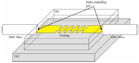
Design and Fabrication of a Long-range Surface Plasmon Polariton Wave Guide for near-infrared light
 Design and Fabrication of a Long-range Surface Plasmon Polariton Wave Guide for near-infrared light Diplomarbeit von Johannes Trapp Design and Fabrication of a Long-range Surface Plasmon Polariton Wave
FANO PLASMONICS MADE SIMPLE
 Higher-order resonances in single-arm nanoantennas: Evidence of Fano-like interference FANO PLASMONICS MADE SIMPLE F. López-Tejeira, R. Paniagua-Domínguez, R. Rodríguez-Oliveros José A. Sánchez-Gil, Instituto
pss Nanocoax solar cells based on aligned multiwalled carbon nanotube arrays solidi physica status
 reprint Phys. Status Solidi A 208, No. 4, 924 927 (2011) / DOI 10.1002/pssa.201026781 Nanocoax solar cells based on aligned multiwalled carbon nanotube arrays T. Paudel 1, J. Rybczynski 2, Y. T. Gao 2,
Vacuum deposition of TiN
 J.Lorkiewicz DESY.27.10.02 Vacuum deposition of TiN (TiN coating of high power coupler elements as an anti-multipactor remedy at DESY) The scope of the project: - reducing secondary electron emission and
Automated High-Throughput Assembly for Photonic Packaging
 Automated High-Throughput Assembly for Photonic Packaging IBM Assembly and Test - Bromont IBM Research - Watson / TRL P. Fortier N. Boyer A. Janta-Polczynski E. Cyr R. Langlois Y. Yoshi H. Numata T. Barwicz
Surface Plasmon Resonance-like integrated sensor at terahertz frequencies for gaseous analytes.
 Surface Plasmon Resonance-like integrated sensor at terahertz frequencies for gaseous analytes. Alireza Hassani and Maksim Skorobogatiy maksim.skorobogatiy@polymtl.ca www.photonics.phys.polymtl.ca Engineering
Challenges and Future Directions of Laser Fuse Processing in Memory Repair
 Challenges and Future Directions of Laser Fuse Processing in Memory Repair Bo Gu, * T. Coughlin, B. Maxwell, J. Griffiths, J. Lee, J. Cordingley, S. Johnson, E. Karagiannis, J. Ehrmann GSI Lumonics, Inc.
Plasmonic Probe With Circular Nano-Moat for far-field Free Nanofocusing
 Zhang and Wang Nanoscale Research Letters (2016) 11:421 DOI 10.1186/s11671-016-1619-y NANO EXPRESS Plasmonic Probe With Circular Nano-Moat for far-field Free Nanofocusing Mingqian Zhang 1* and Tianying
International Journal of Scientific & Engineering Research, Volume 6, Issue 2, February-2015 ISSN PHOTONIC CRYSTAL FIBER- AN OVERVIEW
 45 PHOTONIC CRYSTAL FIBER- AN OVERVIEW Neha Mahnot1, Shikha Maheshwary2, Rekha Mehra3 1, 2, 3 Govt. Engg. College, Ajmer 2 shikhasm1992@gmail.com 1 neha29mahnot@gmail.com Abstract- This review paper gives
Optical fibers. Laboratory of optical fibers. Institute of Photonics and Electronics AS CR, v.v.i.
 Optical fibers Laboratory of optical fibers Institute of Photonics and Electronics AS CR, v.v.i. http://www.ufe.cz/en/laboratory-optical-fibres n 1 n 1 > n 2 Waveguiding principle optical fiber W. Snell
Sheet) Graphite Sheet
 Graphite Sheet") PGS(Pyrolytic Graphite Sheet) Graphite Sheet Panasonic Electronic Device Co.,Ltd Panasonic Electronic Device Hokkaido Co.,Ltd PGS Graphite Sheet PGS (Pyrolytic Highly Oriented Graphite Sheet) is made of
PGS(Pyrolytic Graphite Sheet) Graphite Sheet Panasonic Electronic Device Co.,Ltd Panasonic Electronic Device Hokkaido Co.,Ltd PGS Graphite Sheet PGS (Pyrolytic Highly Oriented Graphite Sheet) is made of
Surface plasmon polariton mediated emission of light from top-emitting organic light-emitting diode type structures
 Organic Electronics 8 (2007) 136 147 www.elsevier.com/locate/orgel Surface plasmon polariton mediated emission of light from top-emitting organic light-emitting diode type structures S. Wedge a, *, A.
Infrared surface plasmon resonance biosensor
 Infrared surface plasmon resonance biosensor Justin W. Cleary, 1 Gautam Medhi, 1 Monas Shahzad, 1 Robert E. Peale, 1 * Walter R. Buchwald, 2 Sandy Wentzell, 2 Glenn D. Boreman, 3 Oliver Edwards, 4 and
High Speed Serial Link (HSSL) Channel Modeling. CST workshop series 2010 February 10 1
 Channel Modeling. CST workshop series 2010 February 10 1") High Speed Serial Link (HSSL) Channel Modeling www.cst.com CST workshop series 2010 February 10 1 Outline Introduction HSSL design workflow Creating a HSSL model Simulating a HSSL HSSL modeling example
High Speed Serial Link (HSSL) Channel Modeling www.cst.com CST workshop series 2010 February 10 1 Outline Introduction HSSL design workflow Creating a HSSL model Simulating a HSSL HSSL modeling example
PLASMONICS. The Promise of
 A technology that squeezes electromagnetic waves into minuscule structures may yield a new generation of superfast computer chips and ultrasensitive molecular detectors The Promise of PLASMONICS By Harry
Alternative Approaches to 3-Dimensional Packaging and Interconnection
 Alternative Approaches to 3-Dimensional Packaging and Interconnection Joseph Fjelstad SiliconPipe, Inc. www.sipipe.com IC Packaging a Technology in Transition In the past, IC packaging has been considered
NANO SCRATCH TESTING OF THIN FILM ON GLASS SUBSTRATE
 NANO SCRATCH TESTING OF THIN FILM ON GLASS SUBSTRATE Prepared by Jesse Angle 6 Morgan, Ste156, Irvine CA 92618 P: 949.461.9292 F: 949.461.9232 nanovea.com Today's standard for tomorrow's materials. 2010
Optimization of optical performances in submicron silicon-on-insulator rib and strip waveguides by H 2 thermal annealing
 I N S T I T U T D E R E C H E R C H E T E C H N O L O G I Q U E Optimization of optical performances in submicron silicon-on-insulator rib and strip waveguides by H thermal annealing Erwine Pargon 1, Cyril
Confocal Microscopy of Electronic Devices. James Saczuk. Consumer Optical Electronics EE594 02/22/2000
 Confocal Microscopy of Electronic Devices James Saczuk Consumer Optical Electronics EE594 02/22/2000 Introduction! Review of confocal principles! Why is CM used to examine electronics?! Several methods
Corning RC Specialty Fibers Reduced Cladding Fibers Enable Miniaturization and Device Integration
 Corning RC Specialty Fibers Reduced Cladding Fibers Enable Miniaturization and Device Integration Photonic Materials PI1442 Issued: July 2005 Supersedes: August 2003 Featuring ultra-tight specifications,
Theory of resonance and mode coupling in photonic crystal devices
 Theory of resonance and mode coupling in photonic crystal devices Thomas P. White A thesis submitted for the degree of Doctor of Philosophy Centre for Ultrahigh-bandwidth Devices for Optical Systems (CUDOS),
A visible-near infrared tunable waveguide based on plasmonic gold nanoshell
 Vol 17 No 7, July 2008 c 2008 Chin. Phys. Soc. 1674-1056/2008/17(07)/2567-07 Chinese Physics B and IOP Publishing Ltd A visible-near infrared tunable waveguide based on plasmonic gold nanoshell Zhang Hai-Xi(
PUBLISHED VERSION.
 PUBLISHED VERSION Ruan, Yinlan; Afshar Vahid, Shahraam; Monro, Tanya Mary Efficient excitation of surface plasmons in metal nanorods using large longitudinal component of high index nano fibers, Optics
Resonant and non-resonant generation and focusing of surface plasmons with circular gratings
 Resonant and non-resonant generation and focusing of surface plasmons with circular gratings Jennifer M. Steele *, Zhaowei Liu, Yuan Wang, and Xiang Zhang 5130 Etcheverry Hall, NSF Nanoscale Science and
Fs- Using Ultrafast Lasers to Add New Functionality to Glass
 An IMI Video Reproduction of Invited Lectures from the 17th University Glass Conference Fs- Using Ultrafast Lasers to Add New Functionality to Glass Denise M. Krol University of California, Davis 17th
NoE Plasmo-nano-devices. Plasmonics Roadmap
 NoE Plasmo-nano-devices Plasmonics Roadmap Alain Dereux Coordinator of NoE FP6 IST Plasmo-nano-devices adereux@u-bourgogne.fr http://www.plasmonanodevices.org Department of Nanosciences Submicron Optics
Interlayer Dielectric (ILD) Cracking Mechanisms and their Effects on Probe Processes. Daniel Stillman, Daniel Fresquez Texas Instruments Inc.
 Cracking Mechanisms and their Effects on Probe Processes. Daniel Stillman, Daniel Fresquez Texas Instruments Inc.") Interlayer Dielectric (ILD) Cracking Mechanisms and their Effects on Probe Processes Daniel Stillman, Daniel Fresquez Texas Instruments Inc. Outline Probe Optimization Why is it needed? Objective and obstacles
Interlayer Dielectric (ILD) Cracking Mechanisms and their Effects on Probe Processes Daniel Stillman, Daniel Fresquez Texas Instruments Inc. Outline Probe Optimization Why is it needed? Objective and obstacles
Hybrid III-V/Si DFB laser integration on a 200 mm fully CMOS-compatible silicon photonics platform
 Hybrid III-V/Si DFB laser integration on a 200 mm fully CMOS-compatible silicon photonics platform B. Szelag 1, K. Hassan 1, L. Adelmini 1, E. Ghegin 1,2, Ph. Rodriguez 1, S. Bensalem 1, F. Nemouchi 1,
Rare Earth Doped Fibers for Use in Fiber Lasers and Amplifiers
 Photonics Media Webinar: 4 th Nov 2013 Rare Earth Doped Fibers for Use in Fiber Lasers and Amplifiers George Oulundsen, Fiber Product Line Manager Bryce Samson, VP Business Development 1 Outline Introduction
Light manipulation by plasmonic nanostructures
 Light manipulation by plasmonic nanostructures A thesis submitted for the degree of Doctor of Philosophy of the Australian National University Wei Liu July, 2013 Declaration This thesis is an account
Low-loss light transport at the subwavelength scale in silicon nano-slot based symmetric hybrid plasmonic waveguiding schemes
 Low-loss light transport at the subwavelength scale in silicon nano-slot based symmetric hybrid plasmonic waveguiding schemes Yusheng Bian and Qihuang Gong * State Key Laboratory for Mesoscopic Physics,
Plastic Coated Silica/Silica (Low OH) FIBER CROSS SECTION Polyimide and Acrylate Coated. Nylon and Tefzel Coated
 FIBER CROSS SECTION Polyimide and Acrylate Coated. Nylon and Tefzel Coated") DESCRIPTION When looking for a high quality fiber with superior transmission and a numerical aperture (N.A.) of 0.22 for efficient light coupling, the is the fiber of choice. The Anhydroguide fiber is
DESCRIPTION When looking for a high quality fiber with superior transmission and a numerical aperture (N.A.) of 0.22 for efficient light coupling, the is the fiber of choice. The Anhydroguide fiber is
Tackling the optical interconnection challenge for the Integrated Photonics Revolution
 Tackling the optical interconnection challenge for the Integrated Photonics Revolution Dr. Ir. TU Delft, Precision and Microsystems Engineering m.tichem@tudelft.nl Microfabrication and MEMS Si microfabrication
UT Austin, ECE Department VLSI Design 2. CMOS Fabrication, Layout Rules
 2. CMOS Fabrication, Layout, Design Rules Last module: Introduction to the course How a transistor works CMOS transistors This module: CMOS Fabrication Design Rules CMOS Fabrication CMOS transistors are
Diode Pumped Miniature Eye-Safe Laser Q-Switched by Passive Materials
 Diode Pumped Miniature Eye-Safe Laser Q-Switched by Passive Materials Presented at SPIE AeroSense 22 Ruikun Wu, J.D. Myers, M.J. Myers, Christopher R. Hardy Kigre, Inc.1 Marshland Road, Hilton Head Island,
Multiple wavelengths, multiple angles surface plasmon resonance. measurements
 Multiple wavelengths, multiple angles surface plasmon resonance measurements J.-M. Friedt, R. De Palma, W. Laureyn and A. Campitelli IMEC, Kapeldreef 75, 3001 Leuven, Belgium October 8, 2002 78.20.Ci Abstract
Lecture 19 Microfabrication 4/1/03 Prof. Andy Neureuther
 EECS 40 Spring 2003 Lecture 19 Microfabrication 4/1/03 Prof. ndy Neureuther How are Integrated Circuits made? Silicon wafers Oxide formation by growth or deposition Other films Pattern transfer by lithography
1 Introduction. Keywords: double bowtie nanoantenna, ring grating, plasmonic, field enhancement, plasmon-emitter coupling
 Nanospectroscopy 2015; 1: 61 66 Research Article Open Access N. Rahbany, W. Geng, S. Blaize, R. Salas-Montiel, R. Bachelot, C. Couteau* Integrated plasmonic double bowtie / ring grating structure for enhanced
Modification of Glass by FS Laser for Optical/Memory Applications
 Modification of Glass by FS Laser for Optical/Memory Applications Kazuyuki Hirao and Kiyotaka Miura Department of Material Chemistry Kyoto University International Workshop on Scientific Challenges of
NanoSystemsEngineering: NanoNose Final Status, March 2011
 1 NanoSystemsEngineering: NanoNose Final Status, March 2011 The Nanonose project is based on four research projects (VCSELs, 3D nanolithography, coatings and system integration). Below, the major achievements
Sub-micron scale patterning of fluorescent. silver nanoclusters using low-power laser
 Sub-micron scale patterning of fluorescent silver nanoclusters using low-power laser Puskal Kunwar 1,*, Jukka Hassinen 2, Godofredo Bautista 1, Robin H. A. Ras 2, and Juha Toivonen 1 1 Tampere University
ENS 06 Paris, France, December 2006
 CARBON NANOTUBE ARRAY VIAS FOR INTERCONNECT APPLICATIONS Jyh-Hua ng 1, Ching-Chieh Chiu 2, Fuang-Yuan Huang 2 1 National Nano Device Laboratories, No.26, Prosperity Road I, Science-Based Industrial Park,
III-V heterostructure TFETs integrated on silicon for low-power electronics
 In the Quest of Zero Power: Energy Efficient Computing Devices and Circuits III-V heterostructure TFETs integrated on silicon for low-power electronics K. E. Moselund, M. Borg, H. Schmid, D. Cutaia and