PRESENTS PCB Layout for CCA Made Easy Everything You Ever Wanted to Know About Manufacturing but Were Afraid to Ask
|
|
|
- Rosanna Cook
- 6 years ago
- Views:
Transcription


1 PRESENTS PCB Layout for CCA Made Easy Everything You Ever Wanted to Know About Manufacturing but Were Afraid to Ask Phone: Fax: For Information Please Call or
2 Don t t Even Think About DFM Cause I Don t t Do It!
3 Why DFM Fewer Design & Prototype Changes Lower Cost Better Reliability Higher Quality Ensures Success with New / Future Product Introductions A A Richly Rewarding Experience that Motivates Personnel
4 Why Should I Care Designers who take the time to learn and understand PCB manufacturing, CCA manufacturing, and Component manufacturing today will be employed tomorrow. Companies who support a PCB Designer in learning PCB manufacturing, CCA manufacturing, and component manufacturing today will be in business tomorrow. Market Analyst reports show that the company s s that team up with PCB, CCA, and Component manufacturers today will become the companies of the future by gaining significant market share tomorrow. Processes have pushed the envelope on equipment available today. Techniques used by these manufacturing companies may cross over and could become the solution the other was looking for.
5 Ok fine WIIFM? #10 Greater Knowledge Base & Understanding of Mfg. #9 Improved Efficiency By Understanding More #8 More Desirable for a Potential Employer #7 Less Whining by Your M.E. Or C.M. #6 Fewer Design Change Requests = Less Work For You! #5 Less Likely to Become the ME s Scapegoat #4 Still Employed Tomorrow #3 Cost Savings Realized in Mfg. Directly Attributed to You #2 On Time Shipments Directly Attributed to You #1 Able to do More For Less, more profitable, and all due to your improved knowledge = More Pay
6 Now that I Care What is DFM? DFM Means Coordinating Product Design With Mfg. Plant Capabilities to Maximize Efficiency at the Lowest Cost The days of Design Engineers Throwing it Over The Wall to Manufacturing are Over!
7 Where Do We Start? But of Course Where Else At the Executive Level Must lead with a commitment to infuse the corporate culture with DFM s inherent advantages
8 But Wait Don Don t t Stop There! Orchestrate personnel from different job functions Design, manufacturing (please keep in mind that Test is considered Part of Manufacturing throughout this presentation), purchasing, production, management, and distribution. All must have desire to perform with unified vision All must have in-depth understanding of the delicate interrelationships among their job functions All must be capable of understanding the various tradeoffs dictated by DFM and determine at which stages in manufacturing these tradeoffs should happen to benefit the manufacturer and customer
9 SMT A A Crash Course In Manufacturing
10 MAN Improper Training vs. Proper Training vs. No Training MACHINE Not capable Not maintained METHOD Not capable or Improper MATERIALS Bad PCB layout The 4 M sm Garbage In = Garbage Out
11 M.E. AKA Fire Fighter Typical scenario upon arriving to work Line outside office door is 4 deep SMT Line 2 is down due to a broken belt on the machine (operator forgot to do PM) SMT Line 4 is having wetting issues on the PCB s s but product has to ship today can can t you make it solder? SMT Line 6 is having placement issues and has not been running all morning SMT line 8 is having solder paste issues for some reason what do you want us to do? Oh, and by the way all all of the product for all of these lines has to ship by 2pm today or we will be late on our shipment and have to pay a 10% penalty. When do you think you can have it all fixed?
12 A typical cause and effect diagram for the SMT process has well over 100 variables M.E. s s Mission Eliminate as many of these variables as possible Promotes quick and efficient process trouble shooting due to less variables having to be investigated, which aids in on-time shipments Do more for less Ensure process and manufacturing lines are as flexible as possible Everything is inter-changeable even operators
13 Machine TQM (Total Quality Maintenance) A good ME will be a stickler about maintenance Why, because it is one less variable that has to be investigated when trouble shooting process issues Method Process Validation ME will develop a NPI Man ARE you ready! --- AUTOMATE! REGULATE! EDUCATE! Automate as much as possible Where you can t Automate, then Regulate Easiest First Educate...Educating your work force is the cheapest fastest way to reduce cost and improve quality
14 Material Seems Easy But 80% of MFG. Issues typically falls under Materials Designers do it once vs. M.E. does it 10 s of thousands of times A good PCB layout makes material variable elimination simple Allows M.E. to focus on the real material related issues QA gains a better grasp on supplier issues quicker so info can be feedback for improvements Questionable material is not used anyway Purchasing and Component Engineering become more aware that a cost savings at the front of the line is not a true cost savings unless the same savings is shown at the back end of the line
15 SMT MFG LINE Screen Print Reflow Pick & Place
16 Screen Print Process Process Fundamentals Metal Stencil with matching holes (or apertures) line up with pads on PCB that are to be soldered on Solder is deposited through the holes in the stencil with a squeegee blade Thickness of stencil dictates height of deposit (along with several other machine parameters, but deposit height starts here) The object of this process is to deposit the right amount of solder so as to achieve ZERO defects after reflow
17 Process Flow The PCB is placed on a flat, hard, stable surface The stencil is placed over the PCB and the openings on the stencil are lined up with the appropriate pads The solder paste is pushed through the holes on the stencil with a squeegee blade
18 Process Strategy The trick in this process is to be sure that the PCB is perfectly flat so that the stencil can form a perfect gasket to the PCB When the stencil does not form a perfect gasket, several different types of solder printing defects can occur which all lead to defects after the reflow process
19 Manual The PCB is hand placed on a flat tabletop The stencil is placed over the PCB and manually lined up to the PCB The solder paste is hand printed using a hand held squeegee The printed PCB is manually transferred to the next operation Stencil can be 20 x 20 Aluminum tubular or cast and smaller. 29 x 29 stencil would be too large to handle and print properly Support tooling is typically not used for this approach


20 Solder Spheres Solder Paste Stencil Printed Solder Printed Solder
21 Semi-Automated The PCB is hand placed inside the screen-printing system The stencil is loaded inside the system and manually lined up to the PCB The solder paste is automatically printed with squeegee blades mounted inside the machine The printed PCB is manually transferred to the next operation Stencil size is typically 20 X 20 Aluminum tubular. Aluminum cast frame requires a special fixture to mount frame inside machine and typically increases set-up time by 5 to 10 minutes Support tooling is manually placed support pins

22

23
24 The PCB is automatically loaded inside the screen-printing system via a magazine loader and edge conveyor system The stencil is partially hand loaded inside the system and is then automatically pulled into the machine The machine then automatically lines up the PCB to the Stencil via v an upward and downward looking camera, which uses fiducials on the PCB and the Stencil A rising table automatically comes up to support the PCB The solder paste is automatically printed (and dispensed if option on is available) with squeegee blades mounted inside the machine The printed PCB is automatically transferred to the next operation on via an edge conveyor Stencil size can be 29 X 29 or 20 X 20 Aluminum tubular Automated Aluminum cast frame requires a special fixture to mount frame inside machine and typically increases set-up time by 5 to 10 minutes. Support tooling is typically manually placed support pins

25
26 Screen Print Over View Key to good screen print process is creating the gasket between stencil and PCB Number one variable which affects Gasket is Board Support Ideal fixture for Primary (top) side assembly (no components on Secondary (back) side) is flat stable surface Ideal fixture for Secondary (back) side (components on Primary (top) side) is vacuumed formed fixture Ideal Stencil size is 20 X 20 Allows flexibility by quick interchanges between various available processes Max Array sizes are minimized, which are easier to process and manage Stencil Storage is more manageable as compared to the 29 X 29 Overall board size exceeds 20 X 20 then use 29 X 29
27 DFM Design Guide Lines For Screen Print
28 Array Panelization Should the PCB layout Engineer specify this ABSOLUTELY! Don t t just let the PCB house control this A PCB house is only going to optimize the panel size based on their process requirements, and not your CCA houses Panelization should be based on ALL machine capability, Optimized through put on manufacturing line Optimized use of raw materials for both the CCA & PCB fab house PCB layout, CCA Manufacturing, and PCB Fabrication Engineers should all work together to develop a standardized approach
29 Array Standardization 20 X 20 Stencil Minimum array length is 3" (length of array is X direction) Minimum array width is 2.5" (width of array is Y direction) For PCB Thickness =.042" or greater, max length (X) = 14" & max width (Y) = 12 PCB Thickness =.04199" to.014,, max length (X) = 14" & max width (Y) = 6 6 PCB thickness under.014 typically require a carrier for the entire SMT process Array Width (Y) should never exceed Length (X). Makes array too unstable for automated process Weight of components
30 20 x20 x20 Tubular Frame Manufacturers LOGO 15 Long X 11.6 Wide Maximum Printable Area Company Name PCB # xxxxxxx Rev.x Job# xxxxx. / Stencil thickness Side designation / Smallest lead pitch Date Manufactured PCB #. If not supplied with Gerber then please contact ME group for clarification ½ Wide Glue Area 1.0 Wide Mesh Area Center line: This is your centerline of foil. Center artwork from here.
31 Array Standardization Array Standardization A radius should always be used on rail corners Eliminates sharp corners and less likely to cause a problem Standard tooling hole size is /-.001", non-plated, 4 corners. Local Fiducial Fiducial locations, shapes, and sizes are critical for the CCA process, but are typically not used during the PCB fabrication process Global Fiducial Do not use slotted tooling holes!.100 Standard.100 spacing between Spacing PCB's is typically.100 Standard rail width is typically.400
32 Array Standardization Standard Global Fiducials should be.05" (round) plated, and placed on all 4 corners of the array rail with 2X Solder Mask clearance The Primary global fiducials should always mirror the secondary global fiducials Local Fiducials Glad you asked! I ll I take it!
33 Array Standardization Board edge Clearances.020 Scoring Web must be sufficient to allow for the board to be processed through entire CCA process Web thickness is also dependant on the over all board thickness A good web to go with is.011 +/-.003 with a 55 to 60 o angle THE DEPTH OF THE SCORE BETWEEN TOP AND BOTTOM MUST BE WITHIN 0.005" +/-0.001" OF EACH OTHER


34 Reasons For Clearing Board Edges
35 SolderMask Extremely critical for screen print process Biggest mistake seen by board layout engineers COMPENSATING DIMENSIONAL CHARACTERISTICS FOR PCB PROCESS All dimensions should be final dimensions Let PCB fab house compensate for you SolderMask height must be below or even with pad height Non-Solder Mask defined pads are the best Solder Mask defined pads used when pad shape is not defined by design Tent all Via s s whenever possible Clear all solder mask away (as well as traces) from all break-away away areas Use a light Green Solder Mask and stick with the same color solder mask
36 Silkscreen Images IS IT NECESSARY? HECK NO! Folks have gotten lazy Use a Transparency It will Force the CCA house to use the Assembly drawing Less mistakes will be made!
37 Board Thickness PCB material determines Tg Tg = glass transition phase Temperature the material begins to change state is typical FR4 Tg = 140 o C is high Tg FR4 Tg = 170 o C Thin PCB s s must have high Tg material.045 and < thick PCB s s use the Specify for everything if possible No Generic Call Outs on FAB Drawing! Clearly specify material type with 4101 call out
38 Copper Distribution Critical In Reducing Warpage Especially thin multi-layer layer substrates Copper must be distributed evenly 4 Layer PCB Layer 1 & 4 matched Layers 2 & 3 matched 6 Layer PCB Layer 1 & 6 matched Layers 2 & 5 matched Layers 3 & 4 matched
39 Land Creation Standardize! Work with M.E. and Optimize! Use SM782 As Starting Point Only! Validate by Testing! Lead Pitch Must Match Part Spec. Metric = Metric & Inches = Inches Key things to Remember Every solder joint must have 3 sides Larger surface area = more reliable Too large/long of pads results in bridging Think SYMETRICAL Ideal Pin 1 / Polarity Mark = Longer Lead Every 10 th pin for multi-leaded leaded devices.


40 Reasons Lead Pitch Must Match Part Spec.


41 Reasons Lead Pitch Must Match Part Spec.

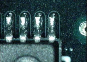
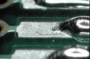
42 Land Creation Gull Wing Device Needs No toe fillet Pads do not need to extend in front of toe Remember - 3 sides to a solder joint so give it a toe fillet How much? Take the Thickness of the lead and multiple by the size of the fillet you would like to achieve i.e. i.e. you want a 50% fillet and the lead is.020 thick..5 X.020 =.01 Side fillet Pitch of the device limits you You will always need at least 1 mil on either side 50% Heel fillet Needed (Class 2) Pad extends underneath device Usually does not affect real estate (as much!) Extend pad length pass the heel of the device at least.20 to Can get away with a.015 extension if necessary. To much room can lead to shifting of the part from side to side Just the right amount allows the device to self-center
43 TENT THEM! TOO BIG, THEN FORGET IT! 13.5mil hole stacked 3 high for drilling 12mil hole stacked 2 high for drilling 10mil hole drilled 1 at time Small drill bits wander Affects cost Via Size


44 Reasons for Complete Via Tenting


45 More Reasons for Tenting Via s
46 HASL Surface Finish HASL Board Houses Sub-Out Their HASL Process Most HASL Shops Lack Process Controls If it didn t t solder the first time (probably due to dirty copper) they send it back through Each thermal excursion affects PCB MTBF rate HASL Shops Do Not Properly Maintain Solder Bath Copper level is too high, which causes Dewetting Dewetting? No turning back It can t t be fixed! HASL Hides Real Issues Solderability testing absolute must!


47 Reasons For Solderability Testing
48 Silver Surface Finish Silver Immersion -- Directly Over Copper Silver Molecular Structure Related to Solder Silver Amalgamates into the solder FLAT, FLAT, FLAT! Great Shelf Life Neutral PH Bath at Low Temperatures Silver Migration NO! No one can prove this Silver too thin of coating Silver Won t t Stick to Dirty Copper Great Contrast Allows Naked Eye Detection Silver finish is actually REWORKABLE Silver can be removed, copper cleaned, and re-coated


49 Silver Surface Finish Silver Won t t Stick to Dirty Copper Great Contrast Allows Naked Eye Detection Silver finish is actually REWORKABLE Silver can be removed, copper cleaned, and re-coated
50 Tin Surface Finish Tin Immersion, Here s s my thoughts on it IT SUCKS! JUST SAY NO! DON T T USE IT! Nothing but soldering issues You Will Need Two Things LOTS and LOTS of HIGHLY ACTIVE FLUX Typical Activator is FLORIDE OR CHLORIDE Both Are EXTREMELY CORROSIVE LOTS and LOTS of HEAT Poor Shelf Life Multiple handling issues Hazardous Waste Generated by Bath is Costly


51 Reasons for Avoiding Tin Surface Finish
52 Gold Surface Finish Immersion Gold over Electrolysis-Nickel Can t t get silver then it will have to do Gold is porous does not seal nickel well Nickel will oxidize over time Becomes impervious to solder Typical Max Shelf Life = 3 months Major issues with black pad Sensitive to handling.
53 OSP Surface Finish OSP, Here s s my thoughts on it IT SUCKS! JUST SAY NO! DON T T USE IT! Nothing but soldering issues! Copper Whatever happen to just bare copper? Maybe an ideal approach for a Proto-Type builds


54 OSP Surface Finish
55 PPT Surface Finish PPT or Precision Pad Technology Patented Solid Solder Deposit Process Solder Coating Over Copper with mesh impression CCA does gross print with tacky flux Phenomenally better End Results 100% Yields Every Single Time PPT Passed HALT & HASS Testing Ideal for: Pad & Laminate Tore while solder joint remained in tact Parts with a pitch of.015 or less ubga s with solder spheres.015 or less 0201 devices Cost: 5-cents/Sq. Inch for Single-Sided Sided PCB 10-cents/Sq. Inch for Double-Sided PCB Potential Cost Center for a PCB House Typical Charge for HASL = 1 cent/sq. Inch Catch 22 - If you don t t ask, they don t t offer! So Ask!

56 PPT Surface Finish
57 Part Orientation Apertures Direction VS Solder is Critical Long Thin Holes Easier to Fill Stroke of Squeegee Blade = Device Leads Direction
58 Primary Vs Secondary If Possible Make it Single S Sided Place Odd Shaped on Primary Side Symmetrical Layouts Nice Don t t Mirror the Parts!


59 Part Size VS Real-Estate Don t t go crazy on miniaturization! Don t t use an 0402 when there s s room for an 0805 and 0201 s GOOD LUCK! Space the parts and/or use appropriately sized parts based on the available support tooling Rule of thumb is simple use the largest part you can for the available PCB real estate & support tooling
60 SMT MFG LINE Screen Print Reflow Pick & Place
61 Pick & Place Process Process Fundamentals PCB array is loaded into the machine Camera looks at global & Local Fiducials Machines Calculates 0,0 array location based on fiducials System begins picking, aligning, and placing parts Object of process is to pick and place components so as to achieve ZERO defects after reflow
62 Process Flow PCB is placed on flat, hard, stable surface PCB is aligned to 0,0 array reference point Components are picked, aligned, and placed
63 Process Strategy Generate Placement Program from Gerber Machine Set-Up Performed by Capable Operator Machine Placement Accuracy Capable
64 The PCB is hand placed on a flat tabletop Components are laid out on the flat tabletop Components are hand picked with tweezers and hand placed onto the appropriate lands CCA is manually transferred to the next operation Support tooling is typically not used for this approach Manual
65 Semi-Automated The PCB is hand placed inside pick & place system Components are picked and placed either by the machines automated placement head, or manually operated placement head The CCA is manually transferred to the next operation. Support tooling is manually placed support pins The tip of the support pin diameter is typically 1/16 Parts too close will not allow the proper placement of pins

66
67 Automated loading Via Edge Conveyor Automated Rising Support Table Supports PCB during placement process Tooling for this typically manually placed Pick & Placement Overhead Gantry Moves to Pick and Place Location Overhead Gantry Typically Used as line balancer Turret - Board Moves to the head Turret Typically Seen on Chip Shooters Alignment Automated Laser - Scans side of the part and compares Upward Looking Camera looks upward at part Feeders manually placed into position Reels Ideal due to location of feeders Stick(or Tube)- Issues with feeders & packaging Best to have parts tape and reeled Tray - Not always desirable Travel Distance

68

69
70 Pick & Place Over View The PCB must be perfectly flat and as stable as possible Diving Board Feeders Must be Mechanically Stable Pick Position Head/Picking System Must Pull a Good Vacuum Alignment Must Be Within at Least +/-.004
71 DFM Design Guide Lines For Pick & Place
72 Array Panelization Guess what these these requirements are identical to the Screen Print Requirements What s s OK for Screen Print is OK for P&P Standardizing on Overall Board Size Minimizes Required Set-Up Time for P&P Be as Flexible as Possible So You Can Interchange Tooling
73 SolderMask Guess what these these requirements are Identical to the Screen Print Requirements What s s OK for Screen Print is OK for P&P
74 Silkscreen Images Guess what these these requirements are Identical to the Screen Print Requirements What s s OK for Screen Print is OK for P&P
75 Board Thickness Guess what these these requirements are Identical to the Screen Print Requirements What s s OK for Screen Print is OK for P&P Remember Stable Flat Surface! Warped boards won t t lie flat no matter what! Boards that don t t lay flat Become Diving Boards During P&P
76 Copper Distribution Guess what these these requirements are Identical to the Screen Print Requirements What s s OK for Screen Print is OK for P&P
77 Pad Geometry Guess what these these requirements are Identical to the Screen Print Requirements What s s OK for Screen Print is OK for P&P Standardize! Standardize! Standardize! Don t t Forget Machine Placement Accuracy Parts Placed +/ with Placement Accuracy of +/.004 Just Won t t Work!
78 Via Size Guess what these these requirements are Identical to the Screen Print Requirements What s s OK for Screen Print is OK for P&P
79 Surface Finish Guess what these these requirements are Identical to the Screen Print Requirements What s s OK for Screen Print is OK for P&P
80 Part Orientation Direction Part Faces VS Direction it Faces when Placed Remember movement is time and money No Rotation is Ideal Parts in Reel Typically Facing Ideal Direction
81 Primary VS Secondary Guess what these these requirements are Identical to the Screen Print Requirements What s s OK for Screen Print is OK for P&P Smallest Parts Always Placed First
82 Part Size VS Real-Estate Guess what these these requirements are Identical to the Screen Print Requirements What s s OK for Screen Print is OK for P&P The smaller the part the slower Rule of thumb is simple use the largest part you can for the available PCB real estate & support tooling
83 SMT MFG LINE Screen Print Reflow Pick & Place
84 Process Fundamentals Oven Process Based on time VS temperature Dependant on: How Oven Performs M.E. understands thermo-dynamics, metallurgy and raw materials Solder not properly activated by flux will not allow solder to wet to the pad Appears Rough with Scales Solder held in liquidous for too long or too short of time creates large lead/tin intermetallics that become brittle Solder not cooled fast enough create large granular structured solder joint that will fail prematurely
85 PCB Placed On Flat Mesh Belt or Pin Chain conveyor Process Flow Mesh Belt/Pin Chain Speed Set To Achieve Optimum Time in Oven Product Travels Through Oven Entering Each Heating Stage at Appropriate Time Heats Assembly Enough for Solder to Reflow Product Continues Through Cooling Section Where Cool Air is Blown Over the Assembly
86 Oven Profile Based on Total Mass Density, Solder, Flux 90 Second Pre-Heat (2.5 0 C/min max ramp rate) 90 Second Soak Temperature (soak temperature depends flux) Soak Process Used to Equalize Temperature Minimizes Thermal Shock and CTE Issues Second Reflow Temperature Quickly Spiked 30 0 C Above Eutectic Point Quickly Cooled Process Strategy The Faster the Better Creates Tighter Grain Structure 4-minute Oven profiles Ideal! Take Heated Length of Oven & Divide By 4 = belt speed Longer Ovens Allow For Better Equalized Temperature
87 Hot Air Convection IR Oven Methods Blowers force air over heating coils producing hot air Hot Air Continues to Flow Over CCA s Infra-Red Heating No Air Sensitive to Colors. Works Well With Flex Circuitry Convection-IR combo Most Common Ideal for CCA on Standard Rigid PCB s Vapor Phase Uses a Flourinert fluid that boils at a specific temperature Works Well on Substrates That Absorb a lot of Heat
88 Laser Soldering / Selective Soldering Ideal for Selective Soldering of Sensitive Devices Expensive, but Worth it if Volume Supports it Hot Bar Oven Methods Hot Bar Comes Down On Area Requiring Soldering Typically Used with Flex Circuitry Air Pressure Pulsing in Vacuum Chamber Vacuum-Sealed, Nitrogen Atmosphere Chamber Pressure in Chamber Varied Causing Solder to Pulse Referred to as a Flux-Less Soldering System Ideal for Hermetically Sealed Devices

89

90
91 Belt Speed Delta T Oven Over View 4 min. profile is ideal Take heated length of the oven & divide by 4 for belt speed Adjust Belt Speed When Density of CCA Does Allow Proper Reflow By Adjusting Zone Settings Only Belt must be stable and not vibrate. Temperature Difference Across Belt Ideally should be within 4 o C If Too Great it Causes Uneven Heating / Reflow Faulty Oven Seals Affect Delta T and Causes Heat Loss Heating System Quick Response Time to Changes Within the Chamber Faster Response Times Allow Better Heat Control For Load Changes Proper Oven Maintenance Ensures Faster Response Times
92 DFM Design Guide Lines For Oven / Reflow
93 Array Panelization Guess what these these requirements are Identical to the Screen Print Requirements What s s OK for Screen Print is OK for Reflow Standardizing on Overall Board Size Minimizes the Number of Reflow Profiles Required Be as Flexible as Possible So You Can Interchange Profiles
94 SolderMask Guess what these these requirements are Identical to the Screen Print Requirements What s s OK for Screen Print is OK for Reflow
95 Silkscreen Images Guess what these these requirements are Identical to the Screen Print Requirements What s s OK for Screen Print is OK for Reflow
96 Board Thickness Guess what these these requirements are Identical to the Screen Print Requirements What s s OK for Screen Print is OK for Reflow Remember Stable Flat Surface! Especially While Solder is in Liquidous State
97 Copper Distribution Guess what these these requirements are Identical to the Screen Print Requirements What s s OK for Screen Print is OK for Reflow
98 Pad Geometry Guess what these these requirements are Identical to the Screen Print Requirements What s s OK for Screen Print is OK for Reflow Standardize! Standardize! Standardize! Don t t Forget Surface Tension! Proper Pad Design Promotes Self-Alignment!
99 Via Size Guess what these these requirements are Identical to the Screen Print Requirements What s s OK for Screen Print is OK for Reflow
100 Surface Finish Guess what these these requirements are Identical to the Screen Print Requirements What s s OK for Screen Print is OK for Reflow Nothing like Solder to Solder!
101 Part Orientation Guess what these these requirements are Identical to the Screen Print Requirements What s s OK for Screen Print is OK for Reflow
102 Primary VS Secondary Guess what these these requirements are Identical to the Screen Print Requirements What s s OK for Screen Print is OK for Reflow Evenly Distribute Heat Sinking Parts Minimizes Uneven Heating
103 Part Size VS Real-Estate Guess what these these requirements are Identical to the Screen Print Requirements What s s OK for Screen Print is OK for Reflow Component Size Variation Doesn t t Support Soak Rule of thumb is simple use the largest part you can for the available PCB real estate & support tooling
104 Company Profile Production Analysis & Learning Services is a full turnkey Design,, Manufacturing, Quality, and Maintenance Engineering Consulting Service with problem solving capabilities unique to the Electronic & Microelectronics Assembly Industry. Company Mission Production Analysis & Learning Services' Mission is to Provide Problem P Solving Capabilities Unique to the Electronic & Microelectronics Assembly Industries with the Highest Possible Level of Design, Manufacturing, Quality, Marketing, Sales, and Technical Engineering Support.
105 Production Analysis & Learning Services, LLC Turnkey Engineering Service Provider for the Electronic & Microelectronics Assembly Industries Electronic, Mechanical, & PCB Design Engineering Manufacturing & Industrial Engineering Support Quality Management & ISO Support IPC Certification & Manufacturing Training Support Manufacturing Equipment Maintenance Service Provider Marketing & Web Site Development & Support Database Development & Support Networking Solutions & Analysis Manufacturer Representative For: Amtech Solder Products, Inc. Advanced Metals Technology Inc. is the world leader in manufacturing electronic grade solder powders Solder Creams Bar Solder Core Wire Flux Righter BGA Spheres SMT Stencil Wipes Bench top Hand Cleaner Soft Wipes Powder and Flux Stay Fresh Packaging Envirosense Inc. Providing Environmentally Safe Chemicals for the Cleaning of Precision and Electronic Assemblies Neutralizer and De-fluxing Cleaner Surface Tension Reducer and Foam Suppresser Tin-Lead Solder and Metal Protection Additive Tsunami Class III Cleaning Machine GC Aero, Inc. Unique Flexible Circuit Applications Single Sided Double Sided Multi-Layer Rigid-Flex Test Laser Quick- Turn & Assembly ifiber Optix, Inc. Delivering tomorrows cable solutions today Custom Designs Fiber Optic Connectors Fiber Optic Adaptors Optical Transceivers Cable Assemblies Fiber Optic Splitters Attenuators Copper Assemblies Distribution Enclosures Total Coax Assemblies 100% Tested Cisco Approved Supplier Private Labeling 24 Hour Turn Lewis and Clark Matching Buyers and Sellers of Pre-owned Equipment Asset management of excess systems Plant Liquidations Reconditioning Field Service Training and Assistance in Leasing and Financing Complete examination Performance testing Analysis of repairs required Total reconditioning Mask Technology, Inc. Service Company for the PCB, Assembly, & Microelectronics Industries Solid Solder Deposit (SSD) - Macro Planar Deposits for Rigid or Flex Substrates SSD Reflow Equipment - Reflow System using PPT Technology Solder Spheres - Solder Spheres for BGA & Chip Scale Packages Wafer Bumping - to.005" sphere size.008" Pitch
106 Marketing Packaging Design Web Development Support Logo Digitizing Production Analysis & Learning Services is capable of providing the following engineering support & services: Electronic & Mechanical Engineering Design Adherence to MIL-STD, IPC, ISO, JDEC, & IEEE Specification Project Engineering Support Turn Key Design to Market Capability Manufacturing & Industrial Engineering Support Supply Chain Management Support Lean Manufacturing Implementation and Support Manufacturing and Production Analysis Reflow Process Development ubga process & rework development Work Instruction Development & Training Hazardous Materials Control & Training Quality Engineering Support Cost of Quality Analysis ISO Certification Assistance Work Instruction Development ISO Training Program SPC Implementation and Training Certification & Training Support Certified IPC (610, 600, & J-STD-001) Training and Testing ESD Training Program
PCB Production Process HOW TO PRODUCE A PRINTED CIRCUIT BOARD
 NCAB Group Seminars PCB Production Process HOW TO PRODUCE A PRINTED CIRCUIT BOARD NCAB GROUP PCB Production Process Introduction to Multilayer PCBs 2 Introduction to multilayer PCB s What is a multilayer
SMT Quick-Tips: selecting a wave. Robert Voigt, DDM Novastar
 SMT Quick-Tips: selecting a wave soldering system Robert Voigt, DDM Novastar Selecting A Wave Soldering System The various types of through-hole (or thru-hole) soldering techniques are: 1. Manual 4. Wave
SMT Quick-Tips: selecting a custom or used machine. Robert Voigt, DDM Novastar
 SMT Quick-Tips: selecting a custom or used machine Robert Voigt, DDM Novastar When to Consider a Custom or Used Machine Let s say you have an unusual product configuration, a unique space requirement,
Advances in Printing nano Cu and Using Existing Cu Based Manufacturing Processes. Michael J. Carmody Chief Scientist, Intrinsiq Materials
 Advances in Printing nano Cu and Using Existing Cu Based Manufacturing Processes Michael J. Carmody Chief Scientist, Intrinsiq Materials Why Use Copper? Lower Cost than Silver. Print on Numerous Substrates.
Basic PCB Level Assembly Process Methodology for 3D Package-on-Package
 Basic PCB Level Assembly Process Methodology for 3D Package-on-Package Vern Solberg STC-Madison Madison, Wisconsin USA Abstract The motivation for developing higher density IC packaging continues to be
IMPACT OF MICROVIA-IN-PAD DESIGN ON VOID FORMATION
 IMPACT OF MICROVIA-IN-PAD DESIGN ON VOID FORMATION Frank Grano, Felix Bruno Huntsville, AL Dana Korf, Eamon O Keeffe San Jose, CA Cheryl Kelley Salem, NH Joint Paper by Sanmina-SCI Corporation EMS, GTS
Optimizing the Insulated Metal Substrate Application with Proper Material Selection and Circuit Fabrication
 Abstract Optimizing the Insulated Metal Substrate Application with Proper Material Selection and Circuit Fabrication Dave Sommervold, Chris Parker, Steve Taylor, Garry Wexler. The Bergquist Company Prescott,
Fairchild Semiconductor Application Note January 2001 Revised September Using BGA Packages
 Introduction AN-5026 Demanding space and weight requirements of personal computing and portable electronic equipment has led to many innovations in IC packaging. Combining the right interface and logic
Failure Modes in Wire bonded and Flip Chip Packages
 Failure Modes in Wire bonded and Flip Chip Packages Mumtaz Y. Bora Peregrine Semiconductor San Diego, Ca. 92121 mbora@psemi.com Abstract The growth of portable and wireless products is driving the miniaturization
MRSI-175Ag Epoxy Dispenser
 MRSI-175Ag Epoxy Dispenser Applications: Microwave & RF Modules MEMS Semiconductor Packaging Multi-Chip Modules Hybrid Circuits Optical Modules Overview The MRSI-175Ag Conductive Epoxy Dispenser handles
The hand soldering process can therefore be defined by the following steps ;
 Hand Soldering with Lead Free Alloys Introduction As companies start to implement lead free soldering processes, hand soldering and associated techniques have been identified as key functions in the manufacturing
SMT Quick-Tips: selecting a pick and place machine. Robert Voigt, DDM Novastar
 SMT Quick-Tips: selecting a pick and place machine Robert Voigt, DDM Novastar How To Select A Pick And Place Machine A Pick and Place machine is the second step in a paste, place, reflow assembly operation.
WELCOME. It is our policy to exceed our customers' expectations. To fulfill this mission we each take personal responsibility for everything we do.
 WELCOME To It is our policy to exceed our customers' expectations. To fulfill this mission we each take personal responsibility for everything we do. Markets Served Military Medical Industrial LED Lighting
EPOXY FLUX MATERIAL AND PROCESS FOR ENHANCING ELECTRICAL INTERCONNECTIONS
 As originally published in the SMTA Proceedings. EPOXY FLUX MATERIAL AND PROCESS FOR ENHANCING ELECTRICAL INTERCONNECTIONS Neil Poole, Ph.D., Elvira Vasquez, and Brian J. Toleno, Ph.D. Henkel Electronic
Wafer Level Chip Scale Package (WLCSP)
") Freescale Semiconductor, Inc. Application Note Document Number: AN3846 Rev. 4.0, 8/2015 Wafer Level Chip Scale Package (WLCSP) 1 Introduction This application note provides guidelines for the handling
Freescale Semiconductor, Inc. Application Note Document Number: AN3846 Rev. 4.0, 8/2015 Wafer Level Chip Scale Package (WLCSP) 1 Introduction This application note provides guidelines for the handling
!"#$#%&#'(() ) **+,-./01)2-,-.3)456,1) /0! **)
 ) **+,-./01)2-,-.3)456,1) /0! **)") !"#$#%&#'(() ) **+,-./01)2-,-.3)456,1) /0!7.5853-09**) Etching Removal of unwanted or non-circuit copper from board Etch resists organic and metallic resists photoresist tin, gold, nickel, silver and alloys
!"#$#%&#'(() ) **+,-./01)2-,-.3)456,1) /0!7.5853-09**) Etching Removal of unwanted or non-circuit copper from board Etch resists organic and metallic resists photoresist tin, gold, nickel, silver and alloys
Taking the LED Pick and Place Challenge
 Taking the LED Pick and Place Challenge Joshua J. Markle Cree, Inc. Joshua_markle@cree.com Abstract For the past few years there has been a shift in the Lighting Industry that has carried over to the surface
SURFACE MOUNT ASSEMBLY OF MINI-CIRCUITS COMPONENTS
 Application Note AN-40-014 SURFACE MOUNT ASSEMBLY OF MINI-CIRCUITS COMPONENTS DATE ISSUED: January 4, 2012 AN-40-014 Rev.: A M150261 (04/14/15) File: AN40014.doc Page 1 of 10 1.0 Introduction Mini-Circuits
Re tinning Components for Hi Rel Assembly
 Hi rel Soldering Re tinning Components for Hi Rel Assembly Alan Cable, President, ACE Production Technologies Lead tinning has experienced a surge in popularity recently for a number of reasons, even though
White Paper Quality and Reliability Challenges for Package on Package. By Craig Hillman and Randy Kong
 White Paper Quality and Reliability Challenges for Package on Package By Craig Hillman and Randy Kong Background Semiconductor technology advances have been fulfilling Moore s law for many decades. However,
DESIGN FOR MANUFACTURABILITY AND ASSEMBLY (DFMA) 1.0 Scope
 1.0 Scope") 1.0 Scope This document prescribes requirements for design for manufacturability and assembly. The manufacturing issues covered are drawn from a list of findings from investigations of non conformances
1.0 Scope This document prescribes requirements for design for manufacturability and assembly. The manufacturing issues covered are drawn from a list of findings from investigations of non conformances
Component Palladium Lead Finish - Specification Approved by Executive Board 1997-xx-xx August 22 Version
 Component Palladium Lead Finish - Specification Approved by Executive Board 1997-xx-xx August 22 Version Appendices 1. User Commitment Form 2. Supplier Compliance Form Table of contents 1. Background 2.
Type III is most commonly used Paste. Finer pitch devices generally require finer metal particle sizes
 Benefits of SPI Use Powder Particle Size Effects of Changes in Particle Size Distribution Type III is most commonly used Paste. Finer pitch devices generally require finer metal particle sizes Disadvantages
Flexible Printed Circuits Design Guide
 www.tech-etch.com/flex Flexible Printed Circuits Design Guide Multilayer SMT Assembly Selective Plating of Gold & Tin-Lead Fine Line Microvias Cantilevered & Windowed Leads 1 MATERIALS CONDUCTOR Copper
Panel Installation Guide
 Panel Installation Guide Tool List: 1. Trowel A 1/32 or 1/16 inch square-notched trowel. You will be using this to spread out the glue. Remember to clean your trowel after each use. 2. Floor Roller This
Process & Capability Manual (Vol )
") Process & Capability Manual (Vol. 12-2015) Seite 1 von 13 1 CHAPTER OVERVIEW 1 CHAPTER OVERVIEW... 2 2 MICROCIRTEC A SHORT PROFILE... 3 2.1 WHO WE ARE... 3 2.2 OBJECTIVES & MARKETS... 3 2.3 DECLARATION
Process & Capability Manual (Vol. 12-2015) Seite 1 von 13 1 CHAPTER OVERVIEW 1 CHAPTER OVERVIEW... 2 2 MICROCIRTEC A SHORT PROFILE... 3 2.1 WHO WE ARE... 3 2.2 OBJECTIVES & MARKETS... 3 2.3 DECLARATION
Precision Engineered Parts
 Precision Engineered Parts Photoetching Laser Cutting Forming Finishing Thin Metal Parts Flexible Circuits EMI Shielding Gaskets www.tech-etch.com PHOTOETCHING Tech-Etch specializes in the manufacture
AMERICAS Tel or Tel CHINA, SHENZHEN Tel
 www.uic.com email: universal@uic.com AMERICAS Tel. 1-800-432-2607 or Tel. +1-607-779-7522 CHINA, SHENZHEN Tel. +86-755-2685-9108 CHINA, SHANGHAI Tel. +86-21-6495-2100 EUROPE Tel. +36-23-445-500 2010 Universal
PCB Technologies for LED Applications Application note
 PCB Technologies for LED Applications Application note Abstract This application note provides a general survey of the various available Printed Circuit Board (PCB) technologies for use in LED applications.
Becoming Lead Free. Automotive Electronics. Antonio Aires Soldering Technical Specialist Visteon Corporation - Palmela Plant
 Automotive Electronics Becoming Lead Free Antonio Aires Soldering Technical Specialist Visteon Corporation - Palmela Plant 1 Agenda 1. Leadfree Electronics Drivers 2. Requirements 3. Areas of Impact 4.
global solutions : local support ª Board Level Shields and Contacts
 global solutions : local support ª Board Level Shields and Contacts Laird Technologies is the world-leader in the design and supply of customized performance-critical products for wireless and other advanced
Power quad flat no-lead (PQFN) package
 package") NXP Semiconductors Application Note Document Number: AN2467 Rev. 5.0, 7/2016 Power quad flat no-lead (PQFN) package 1 Purpose This document provides guidelines for handling and assembly of NXP PQFN packages
NXP Semiconductors Application Note Document Number: AN2467 Rev. 5.0, 7/2016 Power quad flat no-lead (PQFN) package 1 Purpose This document provides guidelines for handling and assembly of NXP PQFN packages
Bob Willis Process Guides
 Practical Selection/Problems with SMT Adhesives Bob Willis Surface M ount Technology (SM T) first started with the introduction of mixed technology designs incorporating components mounted on the underside
10 Manor Parkway, Suite C Salem, New Hampshire
 Micro-Precision Technologies (MPT) is an independent manufacturer of hybrid integrated circuits, multichip modules, and high-precision thick film substrates for the military, medical, avionics, optoelectronics,
3M Electrically Conductive Adhesive Transfer Tape 9707
 Technical Data May 2014 3M Electrically Conductive Adhesive Transfer Tape 9707 Product Description 3M Electrically Conductive Adhesive Transfer Tape (ECATT) 9707 is a pressure sensitive adhesive (PSA)
TMS320C6000 BGA Manufacturing Considerations
 TMS320C6000 BGA Manufacturing Considerations David Bell C6000 Applications Team Abstract When designing with a high-density BGA package, it is important to be aware of different techniques that aid in
Understanding Coating Thickness Measurement Helmut Fischer
 Understanding Coating Thickness Measurement Helmut Fischer Many of the materials used in today s products have some sort of coating, whether it s the shiny new paint job on your Lexus, the anodized protection
14. Designing with FineLine BGA Packages
 14. Designing with FineLine BGA Packages S51014-1.0 Chapter 14, Designing with FineLine BGA Packages, replaces AN 114: Designing with FineLine BGA Packages. Introduction As programmable logic devices (PLDs)
Lead-free soldering materials, some considerations. Presented at FHI conference, Gorinchem November 2005
 Lead-free soldering materials, some considerations Presented at FHI conference, Gorinchem November 2005 Outline Present situation in Europe towards RoHS Industry status Lead-free soldering materials Getting
Ceramos Gen 5 Details on Handling and Processing Application Note
 Ceramos Gen 5 Details on Handling and Processing Application Note Abstract This application note provides information on handling and processing of the CERAMOS Gen5 (CUW CFUP). CERAMOS Gen5 CUW CFUP The
TECHNICAL SPECIFICATION
 TECHNICAL SPECIFICATION ABP SERIES OF AUTOMATIC BLISTER PACKAGING MACHINERY Ridat ABP series of machines are some of the most advanced models in the comprehensive range of Ridat blister packaging equipment.
Material Selection and Parameter Optimization for Reliable TMV Pop Assembly
 Selection and Parameter Optimization for Reliable TMV Pop Assembly Brian Roggeman, David Vicari Universal Instruments Corp. Binghamton, NY, USA Roggeman@uic.com Martin Anselm, Ph.D. - S09_02.doc Lee Smith,
TECHNICAL DATA SHEET 1 P a g e Revised January 9, 2014
 1 P age Revised January 9, 2014 TAIYO PSR-4000 CC01SE (UL Name: PSR-4000JV / CA-40JV) LIQUID PHOTOIMAGEABLE CURTAIN COAT SOLDER MASK Curtain Coat Application Aqueous Developing Solder Mask RoHS Compliant
FEATURES OPTIONS FEEDERS
 FEATURES OPTIONS FEEDERS Europlacer s enduring strength lies in its continuing ability to deliver innovative placement solutions without degrading the legendary flexibility that made the company a success.
Chips Face-up Panelization Approach For Fan-out Packaging
 Chips Face-up Panelization Approach For Fan-out Packaging Oct. 15, 2015 B. Rogers, D. Sanchez, C. Bishop, C. Sandstrom, C. Scanlan, TOlson T. REV A Background on FOWLP Fan-Out Wafer Level Packaging o Chips
Validated Test Method to Characterize and Quantify Pad Cratering Under Bga Pads on Printed Circuit Boards
 Validated Test Method to Characterize and Quantify Pad Cratering Under Bga Pads on Printed Circuit Boards Mudasir Ahmad, Jennifer Burlingame, Cherif Guirguis Technology and Quality Group Cisco Systems,
KGC SCIENTIFIC Making of a Chip
 KGC SCIENTIFIC www.kgcscientific.com Making of a Chip FROM THE SAND TO THE PACKAGE, A DIAGRAM TO UNDERSTAND HOW CPU IS MADE? Sand CPU CHAIN ANALYSIS OF SEMICONDUCTOR Material for manufacturing process
TITAN Quadcopter Assembly Instructions 1
 TITAN Quadcopter Assembly Instructions Even if you have built a multirotor before; please read these instructions carefully! There are a lot of tricks in here that can save you headaches in the future
THE SEVEN SINS OF LEAD FREE SOLDERING TRAINING CERTIFICATION TEST (DVD-70C) v.2
 v.2") This test consists of twenty multiple-choice questions. All questions are from the video: The Seven Sins of Lead Free Soldering (DVD-70C). Each question has only one most correct answer. Circle the letter
This test consists of twenty multiple-choice questions. All questions are from the video: The Seven Sins of Lead Free Soldering (DVD-70C). Each question has only one most correct answer. Circle the letter
LEAD FREE ALLOY DEVELOPMENT
 LEAD FREE ALLOY DEVELOPMENT Karl F. Seelig, VP of Technology AIM Cranston, RI. USA. kseelig@aimsolder.com Abstract. When lead-free solders were first introduced to the electronics industry in the early
Welcome to the Real World of Lead Free Soldering
 Welcome to the Real World of Lead Free Soldering Metallic Resources, Inc. Howard Stevens Nimal Liyanage,, Ph.D Objective: to Provide Education Regarding the Effects of Various Lead Free Soldering Alloys
Following this guideline enables proper treatment of the relays during the critical phase in the relay life.
 Electromechanical relays are one of the most robust and most reliable electronic components. In order to achieve and guarantee the excellent performance of AXICOM relays, some precautions must be taken
Characteristics of Solder Paste
 Characteristics of Solder Paste Flow Solder paste is a viscous non-newtonian fluid, whose resistance to flow is not constant, and which exhibits shear thinning. This is an essential requirement for printing,
3 Thermally Conductive Tapes
 3 Thermally Conductive Tapes Technical Data July, 21 Product Description 3M Thermally Conductive Tapes 885, 881, and 8815 are designed to provide a preferential heat-transfer path between heat-generating
TAIYO PSR-4000 LDI (US) (UL Name: PSR-4000 JA / CA-40 JA)
 (UL Name: PSR-4000 JA / CA-40 JA)") TAIYO PSR-4000 LDI (US) (UL Name: PSR-4000 JA / CA-40 JA) LASER DIRECT IMAGING SOLDER MASK For LDI Exposing Available in Green, Blue, Black and Red Satin Finish Halogen-Free RoHS Compliant Compatible with
TAIYO PSR-4000 LDI (US) (UL Name: PSR-4000 JA / CA-40 JA) LASER DIRECT IMAGING SOLDER MASK For LDI Exposing Available in Green, Blue, Black and Red Satin Finish Halogen-Free RoHS Compliant Compatible with
DSP 798LF (Sn42/Bi58) LEAD FREE WATER SOLUBLE SOLDER PASTE
 LEAD FREE WATER SOLUBLE SOLDER PASTE") LF217. 798LF Rev.A TECHNICAL DATA SHEET TECHNICAL SPECIFICATIONS LF217. 798LF Rev DSP 798LF (Sn42/Bi58) LEAD FREE WATER SOLUBLE SOLDER PASTE CORPORATE HEADQUARTERS USA: 315 Fairbank St. Addison, IL 630-628-8083
LF217. 798LF Rev.A TECHNICAL DATA SHEET TECHNICAL SPECIFICATIONS LF217. 798LF Rev DSP 798LF (Sn42/Bi58) LEAD FREE WATER SOLUBLE SOLDER PASTE CORPORATE HEADQUARTERS USA: 315 Fairbank St. Addison, IL 630-628-8083
Quality in Electronic Production has a Name: Viscom. System Overview
 Quality in Electronic Production has a Name: Viscom System Overview Successful along the whole line with Viscom Circuit board manufacturing Paste print Finish S3070 AFI-Scan S3054QS Paste print Thick film
INTERFLUX ELECTRONICS NV
 Reflow soldering temperature profiling Min : 30sec Max : 120sec Max : +4 C/sec Max : 250 C Min : 230 C Min: +0,5 C/sec Min : +1 C/sec Max : +3 C/sec Max : +1 C/sec Max : -6 C/sec Min : -2 C/sec Min : +1
Design for Flip-Chip and Chip-Size Package Technology
 Design for Flip-Chip and Chip-Size Package Technology Vern Solberg Solberg Technology Consulting Madison, Wisconsin Abstract As new generations of electronic products emerge they often surpass the capability
MY500 Jet Printing. Experience new levels of printing freedom
 MY500 Jet Printing Experience new levels of printing freedom MY500 jet printing flexibility for Faster, higher flexible profitability. MY500 jet printing for Improve customer service with faster response
GRAPHIC MANUFACTURING CAPABILITY Q217-18
 All features are design dependent and may not be achievable in combination Reduced Yield / Special values up ( or down ) to the standard limit are design and application dependent Standard features only
COFAN USA. Meeting your Project needs.
 COFAN USA Meeting your Project needs www.cofangroup.com PCB Substrate Pre-preg Category SEKISUI Laird T-Clad Denka PCB Substrate Pre-preg Category In the PCB industry, there are a couple major Pre-preg
Ceramic Column Grid Array Design and Manufacturing Rules for Flight Hardware
 GODDARD TECHNICAL STANDARD GSFC-STD-6001 Goddard Space Flight Center Approved: 02-22-2011 Greenbelt, MD 20771 Expiration Date: 02-22-2016 Superseding GSFC-STD-XXXXR Ceramic Column Grid Array Design and
UVTOP280-FW-SMD. Description. Maximum Rating (T CASE = 25 C) Electro-Optical Characteristics (T CASE = 25 C, I F = 20 ma)
 Electro-Optical Characteristics (T CASE = 25 C, I F = 20 ma)") v2.0 11/2017 UVTOP280-FW-SMD Deep Ultraviolet Light Emission Source 285 nm, 2.0 mw 3535 Ceramic SMD Package Low Thermal Resistance Chemical and Biological Analysis Description UVTOP280-FW-SMD is a deep
v2.0 11/2017 UVTOP280-FW-SMD Deep Ultraviolet Light Emission Source 285 nm, 2.0 mw 3535 Ceramic SMD Package Low Thermal Resistance Chemical and Biological Analysis Description UVTOP280-FW-SMD is a deep
AN INSTALLED TAPE AUTOMATED BONDING UNIT
 Electrocomponent Science and Technology 1980, Vol. 6, pp 159-163 0305-3091/80/0604-0159 $04.50/0 (C) 1980 Gordon and Breach Science Publishers, Inc. Printed in Great Britain AN INSTALLED TAPE AUTOMATED
Workshop Series 2016
 Workshop Series 2016 Hands-on Approach to Cycle Time Reduction and Productivity Improvement Vishu Shah, Consultek Consulting Group April 21, 2016 ENGEL North America California Technical Center Corona
3M Electromagnetic Compatible Products
 3M Electromagnetic Compatible Products Selection Guide Revision E 3 Innovation Faster, smaller, lighter, easier the skyrocketing development of today s electronics requires new solutions for significant
Lead Free No Clean Solder Paste 4900P Technical Data Sheet 4900P
 Description MG Chemicals has developed a unique flux system designed specifically for high temperature lead free alloys. It provides the fluxing activity levels that promote thermal stability and prevents
Topview 5630 Red SMD LED
 Topview 5630 Red SMD LED 1. Features - Chip High-Luminosity SMD LED - 5.6 x 3.0 x 0.9 mm (L x W x H), 4-Pin, Small Size Surface Mount Type - Wide Viewing Angle - Long Operating Life - MSL 3 2. Applications
contaminated, or if the location of the assembly house is well above sea level.
 VAPOR PHASE REFLOW S EFFECT ON SOLDER PASTE RESIDUE SURFACE INSULATION RESISTANCE Karen Tellefsen. Mitch Holtzer, Corne Hoppenbrouwers Alpha Assembly Solutions South Plainfield, NJ, USA Roald Gontrum SmartTech
TOUCH FOIL INSTALLATION GUIDE
 TOUCH FOIL INSTALLATION GUIDE ZYTRONIC THE WORLD AT YOUR FINGER TIPS A SINGLE TOUCH CAN BE THE BEGINNING OF A JOURNEY PG 2 TOUCH FOIL INSTALLATION GUIDE CONTENTS INTRODUCTION... PG 3 SPECIFICATIONS...
NCAB Group PCB Specification
 NCAB Group Seminar no. 9 NCAB Group PCB Specification NCAB GROUP NCAB Group PCB Specification 14 key features for durable and reliable PCB s NCAB GROUP NCAB Group PCB Specification 2 Are all PCB s created
THIN IMMERSION TIN USING ORGANIC METALS
 THIN IMMERSION TIN USING ORGANIC METALS Jim Kenny, Nils Arendt, Bernhard Wessling, and Karl Wengenroth Enthone Inc., A Business of Cookson Electronics West Haven, CT, USA ABSTRACT With the international
Design Rules & DFM for High-Speed Design
 BEYOND DESIGN C O L U M N Design Rules & DFM for High-Speed Design by Barry Olney IN-CIRCUIT DESIGN PTY LTD AUSTRALIA Summary: Rules are necessary for compatibility with target manufacturing equipment
Introduction Conductors. Supply Planes. Dielectric. Vias PCB Manufacturing Process Electronic Assembly Manufacturing Process
 PCBs/Overview Printed Circuit Boards (PCB) Introduction Conductors. Supply Planes. Dielectric. Vias PCB Manufacturing Process Electronic Assembly Manufacturing Process 29/09/2005 EE6471 (KR) 263 PCBs/Overview
CONCRETE STEPS, HANDRAILS, AND SAFETY RAIL
 SUDAS Standard Specifications Division 9 - Site Work and Landscaping Section 9080 - Concrete Steps, Handrails, and Safety Rail CONCRETE STEPS, HANDRAILS, AND SAFETY RAIL PART - GENERAL.0 SECTION INCLUDES
Highly Accelerated Thermal Shock Reliability Testing
 Highly Accelerated Thermal Shock Reliability Testing by Bob E. Neves Microtek Laboratories, Inc. Anaheim CA and Rick B. Snyder Delphi Delco Electronics Systems, Inc. Kokomo IN and Timothy A. Estes Conductor
Additional Information, DS4, May Recommendations for Printed Circuit Board Assembly of Infineon xf (2) BGA and xf (2) SGA Packages
 BGA and xf (2) SGA Packages") Additional Information, DS4, May 2008 Recommendations for Printed Circuit Board Assembly of Infineon xf (2) BGA and xf (2) SGA Packages Edition 2008-05 Published by Infineon Technologies AG 81726 München,
Additional Information, DS4, May 2008 Recommendations for Printed Circuit Board Assembly of Infineon xf (2) BGA and xf (2) SGA Packages Edition 2008-05 Published by Infineon Technologies AG 81726 München,
Effects of SAC Alloy Copper Dissolution Rates on PTH Processes: Cost and performance justify use of certain alternatives to SAC305/405
 Effects of SAC Alloy Copper Dissolution Rates on PTH Processes: Cost and performance justify use of certain alternatives to SAC305/405 1 Craig Hamilton, Polina Snugovsky (Celestica) & Matthew Kelly (IBM)
Flex and Rigid-Flex Printed Circuit Design
 Flex and Rigid-Flex Printed Circuit Design Old Content - visit altium.com/documentation Modified by on 29-Nov-2016 Related Videos Bending Lines Enhanced Layer Stack Management Layer Stack Regions A rigid-flex
INDUSTRIAL GUARDRAIL SYSTEMS
 INDUSTRIAL GUARDRAIL SYSTEMS STRONGEST GUARDRAIL ON THE MARKET MANUFACTURED IN THE U.S.A. BEST PRICES MOST VARIETIES HEAVY DUTY ONE-LINE OR TWO-LINE Posts: 4 Sched 80 pipe Rail: 6 Sched 40 pipe Sleeved
BONDING OF MULTIPLE WAFERS FOR HIGH THROUGHPUT LED PRODUCTION. S. Sood and A. Wong
 10.1149/1.2982882 The Electrochemical Society BONDING OF MULTIPLE WAFERS FOR HIGH THROUGHPUT LED PRODUCTION S. Sood and A. Wong Wafer Bonder Division, SUSS MicroTec Inc., 228 SUSS Drive, Waterbury Center,
Low CTE / High Tg FR-4 with High Heat Resistance
 Low CTE / High Tg FR-4 with High Heat Resistance Laminate: EM-827 Prepreg: EM-827B 1 Features Tg(DSC) > 170 Z direction CTE < 3.0% (50~260 ) High thermal degradation temperature: Td > 340 Excellent thermal
FLEXIBLE & RIGID-FLEX CIRCUITS TECHNICAL ENGINEERING GUIDE. Delivering Quality Since 1952.
 FLEXIBLE & RIGID-FLEX CIRCUITS TECHNICAL ENGINEERING GUIDE Delivering Quality Since 1952. DELIVERING QUALITY SINCE 1952. Epec Engineered Technologies designs and manufactures customized, built-to-print,
Quick Guide. CSN950 MultiHead Dimensioner _v2d_MAN_QG_CSN950MH_EN
 Quick Guide CSN950 MultiHead Dimensioner File: 20160406_v2d_MAN_QG_CSN950MH_EN CSN950 MultiHead Quick Guide Table of Contents 1. Safety Instructions... 2 Safety and General Precautions... 2 2. Specifications
TABLE OF CONTENTS SELECTING AN ENCLOSURE COOLING SYSTEM MANUFACTURER. 3 7 QUALITIES TO LOOK FOR IN A MANUFACTURER Manufacturer Location..
 TABLE OF CONTENTS SELECTING AN ENCLOSURE COOLING SYSTEM MANUFACTURER. 3 7 QUALITIES TO LOOK FOR IN A MANUFACTURER. 4 1. Manufacturer Location.. 4 2. Quality Standards 5 UL Ratings 5 NEMA Ratings 6 Performance
Leveraging the Precision of Electroforming over Alternative Processes When Developing Nano-scale Structures
 VOLUME 4 - ELECTROFORMING Leveraging the Precision of over Alternative Processes When Developing Nano-scale Structures Electrical and mechanical component and subsystem designers generally have five techniques
Post Style with ABS Real Tuff
 Post Style with ABS Real Tuff Mantova s patented Post Shelving with ABS Real Tuff removable shelves have been making life easier for thousands of Australian businesses for more then a decade. Removable
Innovative MID Plating Solutions
 Innovative MID Plating Solutions High Reliability Wire Bond Technique for MIDs Jordan Kologe MacDermid Electronics Solutions jkologe@macdermid.com 1 MacDermid: Specialty Chemical Solutions Over 2000 Worldwide
Alternative Approaches to 3-Dimensional Packaging and Interconnection
 Alternative Approaches to 3-Dimensional Packaging and Interconnection Joseph Fjelstad SiliconPipe, Inc. www.sipipe.com IC Packaging a Technology in Transition In the past, IC packaging has been considered
Packaging and Preservation:
 1 of 4 This specification is provided to inform vendors of Raytheon Systems Company's minimum packaging requirements. This document is superseded by any special requirements listed on drawings or specifications.
Three-Dimensional Molded Interconnect Devices (3D-MID)
") Jörg Frank Three-Dimensional Molded Interconnect Devices (3D-MID) Materials, Manufacturing, Assembly and Applica ons for Injec on Molded Circuit Carriers Sample Pages ISBN 978-1-56990-551-7 HANSER Hanser
Jörg Frank Three-Dimensional Molded Interconnect Devices (3D-MID) Materials, Manufacturing, Assembly and Applica ons for Injec on Molded Circuit Carriers Sample Pages ISBN 978-1-56990-551-7 HANSER Hanser
High Frequency Circuit Materials Attributes John Coonrod, Rogers Corporation
 High Frequency Circuit Materials Attributes John Coonrod, Rogers Corporation Specialty high frequency circuit materials have been used in the PCB industry for decades and for many different reasons. There
PEC (Printed Electronic Circuit) process for LED interconnection
 process for LED interconnection") PEC (Printed Electronic Circuit) process for LED interconnection Higher wattage LED s/ power components or their placement in higher densities, requires a larger dissipation of heat in a more effective
PEC (Printed Electronic Circuit) process for LED interconnection Higher wattage LED s/ power components or their placement in higher densities, requires a larger dissipation of heat in a more effective
Ultralow Residue Semiconductor Grade Fluxes for Copper Pillar Flip-Chip
 Ultralow Residue Semiconductor Grade Fluxes for Copper Pillar Flip-Chip SzePei Lim (Presenter), Jason Chou, Maria Durham, and Dr. Andy Mackie Indium Corporation 1 Outline of Presentation Roadmaps and challenges
Welding Processes. Consumable Electrode. Non-Consumable Electrode. High Energy Beam. Fusion Welding Processes. SMAW Shielded Metal Arc Welding
 Fusion Consumable Electrode SMAW Shielded Metal Arc Welding GMAW Gas Metal Arc Welding SAW Submerged Arc Welding Non-Consumable Electrode GTAW Gas Tungsten Arc Welding PAW Plasma Arc Welding High Energy
LOW TEMPERATURE PHOTONIC SINTERING FOR PRINTED ELECTRONICS. Dr. Saad Ahmed XENON Corporation November 19, 2015
 LOW TEMPERATURE PHOTONIC SINTERING FOR PRINTED ELECTRONICS Dr. Saad Ahmed XENON Corporation November 19, 2015 Topics Introduction to Pulsed Light Photonic sintering for Printed Electronics R&D Tools for