Influences of sample preparation on the indentation size effect and nanoindentation pop-in on nickel
|
|
|
- Paul Haynes
- 6 years ago
- Views:
Transcription
1 University of Tennessee, Knoxville Trace: Tennessee Research and Creative Exchange Doctoral Dissertations Graduate School Influences of sample preparation on the indentation size effect and nanoindentation pop-in on nickel Zhigang Wang Department of Materials Science & Engineering, Recommended Citation Wang, Zhigang, "Influences of sample preparation on the indentation size effect and nanoindentation pop-in on nickel. " PhD diss., University of Tennessee, This Dissertation is brought to you for free and open access by the Graduate School at Trace: Tennessee Research and Creative Exchange. It has been accepted for inclusion in Doctoral Dissertations by an authorized administrator of Trace: Tennessee Research and Creative Exchange. For more information, please contact
2 To the Graduate Council: I am submitting herewith a dissertation written by Zhigang Wang entitled "Influences of sample preparation on the indentation size effect and nanoindentation pop-in on nickel." I have examined the final electronic copy of this dissertation for form and content and recommend that it be accepted in partial fulfillment of the requirements for the degree of Doctor of Philosophy, with a major in Materials Science and Engineering. We have read this dissertation and recommend its acceptance: George Pharr, Robert Mee, Yanfei Gao, Erik Herbert (Original signatures are on file with official student records.) George Pharr, Major Professor Accepted for the Council: Dixie L. Thompson Vice Provost and Dean of the Graduate School
3 INFLUENCES OF SAMPLE PREPARATION ON THE INDENTATION SIZE EFFECT & NANOINDENTATION POP-IN IN NICKEL A Dissertation Presented for the Doctor of Philosophy Degree The University of Tennessee, Knoxville Zhigang Wang May 2012
4 Copyright 2012 by Zhigang Wang. All rights reserved. ii
5 DEDICATION To my wife, parents and children, for their love and support iii
6 ACKNOWLEDGEMENTS I would like to express my sincere appreciation to my major professor Dr. George Pharr for his scientific guidance, encouragement and kindness throughout my study and completion of this dissertation. I am grateful to Dr. Erik Herbert for his valuable suggestions and enormous support in the nanoindentation experiments. I specially thank Dr. Robert Mee, my statistics advisor, for his guidance in statistical analysis and his creative suggestions. I would also like to thank Dr. Yanfei Gao for serving on my committee. I am greatly indebted to the many people that I have worked with and benefited from throughout the study. Foremost of them are: Dr. Hongbin Bei at Oak Ridge National Laboratory (ORNL) who helped me grow the single crystal Ni and also supplied me with single crystal W and a part of single crystal Ni; Professor. Easo George and Mr. Cecil A Carmichael at ORNL for their support in sample preparation; Dr. Murat Özer and Dr. Hanno Weitering in the Department of Physics & Astronomy for their tremendous help in the XPS experiments and data analysis; Dr. John Dunlap for his support in AFM experiment. I would also like to thank Dr. Warren Oliver at Nanomechanics Inc., Professor Ramón León in the Department of Statistics, Joe Pribyl at 3M Abrasive System Division, Professor David Joy of Biochemistry and Cellular and Molecular Biology, Professor Siqun Wang of Department of Forestry, Wildlife & Fisheries. I am also grateful to my fellow graduate students, faculties and staff members in the Department of Materials Science and Engineering and in the Alloy Behavior & Design Group, ORNL, for the wonderful time we spent together. This research was sponsored by the National Science Foundation under contract CMMI iv
7 Abstract Careful experiments were performed with a well characterized indenter to systematically investigate the influences of sample preparation on the indentation size effect (ISE) and nanoindentation pop-in behavior in nickel. The Ni (100) surface was prepared by electropolishing and then damaged in a controlled way by polishing with alumina slurry. The damaged layer was systematically removed in steps by colloidal silica polishing (0.02 µm (micrometer)) with the pop-in behavior statistically characterized and the depth dependence of the hardness measured at each step. AFM observation revealed that the electropolished surface is free from scratches, and has the largest roughness. Numerous scratches were observed on the alumina or silica polished specimens, with smaller particle size led to lower roughness. XPS measurements demonstrate that the colloidal silica particles were not embedded in sample surface. Rather, there is an adsorbed soft layer ~1.2 nm (nanometer) thick and a layer of a Ni compound with a thickness of ~ 0.8 nm on the top surface for each polishing step. With a decreasing thickness of the surface damaged layer, pop-in events start to appear, and the cumulative probability increases until it reaches 100%. The cumulative probability curve shifts to the right with an increase of silica polishing time. Long time silica polishing causes the cumulative probability curve to shift to the right of the electropolished curve. The surface mechanical state for each polishing step can be characterized by the detailed statistics of pop-in behavior. The displacement cut-off for ISE measurements, since the hardness measurement is complex, was found to be ~50nm. With a decreasing thickness of the damaged layer, the H-h curve gradually moved down from the highest hardnesses for alumina polishing to the lowest hardnesses for the electropolished surface. For each polishing condition, the measured hardness increases with decreasing of indentation depth. However, the hardness increase after electropolishing stage is the smallest, and the hardness increase after alumina polishing is the largest. These observations demonstrate that hardness v
8 measurement at small depths is very sensitive to the surface state. The experimental observations are consistent with the mathematical predictions of the Nix-Gao model. vi
9 Table of Contents Chapter 1 Introduction Pop-in during nanoindentation The indentation size effect (ISE) Influence of sample preparation on the ISE Indenter Area-Function Calibration The effect of indenter tip blunting The effect of pop-in Thermal drift Special Issues in Nanoindentation Testing The Nix-Gao Model Objectives Chapter 2 Sample preparation and characterization Growth of single crystal Ni Nanoindentation sample preparation Surface roughness measurement The definition of roughness AFM experiments Statistical characterization of surface roughness Results and Discussion of roughness measurement XPS analysis XPS experiments XPS data analysis Summary of XPS analysis Chapter 3 A robust process for hardness measurement by nanoindentation Instrumental compliance Thermal drift correction Area function calibration Tip radius calibration vii
10 3.5 Continuous Stiffness Measurement on and off Surface detection Location A robust process for hardness measurement and data evaluation Chapter 4 Influences of sample preparation on pop-in behavior and statistical characterization of surface mechanical state Pop-in measurement and tip calibration Results and Discussion Conclusion Chapter 5 Influence of sample preparation on the inentation size effect Monitoring area function: Depth cut-off for ISE measurement Area function Pop-in Surface detection Surface roughness Tip radius Oscillation amplitude effect Location effect Influence of sample preparation on the indentation size effect Assess the Nix-Gao theory for ISE Conclusion Chapter 6 Summary and Future Work References: Appendix Appendix VITA viii
11 List of Tables Table 2.1 Summary of polishing procedures including type of polish, amount of material removed Table 2.2 Arithmetic average roughness (Ra): Table 2.3 Root mean roughness (Rq) Table 2.4 Summary of XPS sample preparation including polishing steps, and type of polishing (#1-electropolished specimen, #2-alumina polished specimen, #3-silica polished specimen) Table 2.5 Elements detected by XPS during sputtering Table 2.6 Summary of peak-fitting results Table 4.1 Summary of polishing procedures including type of polish, amount of material removed, and fraction of indents exhibiting a detectable pop-in Table 5.1 Measured hardness at different depths for each polishing step Table 5.2 List of H 0 2, H 0 2 h*, and h* for each polishing status ix
12 List of Figures Figure 1.1 Schematic of pop-in... 1 Figure1.2 The indentation size effect (ISE) for geometrically self-similar indenters such as a cone or pyramid. Usually hardness (H) increases at small depths (the normal ISE), but some cases of decreasing hardness have also been reported (the reverse ISE). According to continuum plasticity, the hardness should be independent of depth. The hardness is defined as the ratio of the load on the indenter (P) to the projected area of contact of the hardness impression A. The picture is from reference [36] Figure 1.3 ISE data for Cu (111) single crystals obtained in nanoindentation experiments [36]. The classic data of McElhaney et al [55] are frequently cited in modeling efforts, but the data of Liu & Ngan [56] indicate that the magnitude of the ISE is very sensitive to surface preparation. All experiments cited here were performed with a Berkovich indenter Figure 1.4 Indentation size effect data for electropolished Ni (100) and its wear surface by nanoscratch techniques. Cordill el al [66, 67] used a Hysitron TriboIndenter to generate wear patterns as function of load and number of cycles, and obtained these data by MTS Nanoindenter XP with a dynamic contact module (DCM) head and Berkovich diamond indenter tip (with a nominal 50 nm tip radius) (a) Average hardness without a roughness correction. The error bars represent the standard deviation. (b) Average hardness with the roughness correction using the P/S 2 method. The error bars represent the standard deviation Figure 1.5 ISE effect in a Ni(100) single crystal from CSM and partial loading/unloading indentation test [61]. (a) hardness as a function of depth with the corresponding modeled size effect (solid lines) and (b) corresponding Nix-Gao plot for all data Figure 1.6 Schematic representation [36]of the Nix-Gao [75] model for (a) conical indenters and (b) its extension to spherical indenters [76]. In both scenarios, the geometrically necessary dislocations (GNDs) are assumed to reside in a hemispherical region beneath the indenter, whose radius is equal to the radius of contact, a, of the hardness impression. For conical indenters, the GND density is then inversely proportional to the depth of penetration, h, and for spheres, it is independent of depth but inversely proportional to the indenter radius, R Figure 1.7 A plot [36] of H 2 versus 1/h for (a) the (111) Cu data of McElhaney et al. [55] and (b) the (110) Ag data of Ma & Clarke [42], both obtained in nanoindentation experiments with a Berkovich indenter. The extreme linearity of the data has been regarded as the primary evidence for the Nix-Gao mechanism, although there are indications in both data sets that the linearity does not extend to very shallow depths (large 1/h) x
13 Figure 1.8 Plots of H2 vs 1/h of Vickers indentation on annealed and working hardened polycrystalline copper [54]. Nix-Gao model breaks down at small depth Figure 1.9 Depth dependency [36]of the hardness for (a) Ir and (b) MgO obtained with a Berkovich pyramidal indenter plotted as H 2 versus 1/h to examine the adequacy of the Nix-Gao model [76, 77]. The deviation from linearity at small h (large 1/h) has been interpreted to mean that the Nix-Gao model breaks down at small depths of penetration [76, 77, 89]. The solid lines are predictions of CMSG (conventional mechanism-based strain gradient plasticity) theory, assuming that the dislocation density saturates at an upper limit that is determined by curve fitting [89]. GND, geometrically necessary dislocation Figure 1.10 A matrix scheme of the proposed research: the influences of sample preparation on Figure 2.1 Schematic of floating zone furnace [93] Figure 2.2 Schematic illustration of (001) Ni specimen in epoxy mount showing the locations of the Vickers indentations used to assess the amount of material removed in each polishing step. Triangular indents were used to identify the Vicker indents Figure 2.3 Thickness of material removed during polishing with 0.02 µm colloidal silica as a function of polishing time Figure 2.4 schematic of AFM Figure 2.5 Contact mode AFM images of electropolished single crystal Ni (100) under ambient conditions. (a) scan size 30x30µm, (b) scan size 4x4µm (c)scan size 2x2µm.. 39 Figure 2.6 Contact mode AFM images of alumina-polished single crystal Ni (100) under ambient conditions. (a) scan size 30x30µm, (b) scan size 4x4µm (c)scan size 2x2µm.. 41 Figure 2.7 Contact mode AFM images of silica-polished single crystal Ni (100) under ambient conditions. (a) scan size 30x30µm, (b) scan size 4x4µm (c)scan size 2x2µm.. 42 Figure 2.8 Basic components of a monochromatic XPS system [94] Figure 2.9 Schematic of XPS physics-photoelectric effect [94] Figure 2.10 XPS curves of electropolished Ni (100) at different sputtering conditions.. 50 Figure 2.11 XPS curves of alumina polished Ni (100) at different sputtering conditions51 Figure 2.12 XPS curves of silica polished Ni (100) at different sputtering conditions.. 52 Figure 2.13 Thin film model Figure 2.14 The surface layers of Ni samples Figure3.1The S 2 /P of fused silica measured by nanoindentation vs indented depth Figure 3-2 The coefficients of the shape function decided from the area function calibration xi
14 Figure 3.3 comparison of the fitting area function with the ideal area function for perfect Berkovich tip Figure 3.4 Image of the brand new DCM tip, obtained by ADE Phaseshift MicroXAM three-dimensional non-contact optical system Figure 3. 5 Nanoindentation load-displacement curve showing the pop-in behavior of (001) W Figure 3.6 Hertz fitting (red) of the elastic portion (black) of P-h curve in Figure Figure 3.7 The statistical results of ISE measurements on electropolished Ni (100) by threedifferent methods: CSM-on, CSM approach, and CSM-off Figure3.8 The load-displacement curves for CSM-on with different oscillation amplitudes on electropolished Ni(100). Loss of contact and tapping emerges when the amplitude is over 2nm Figure 3.9 CSM hardness measurements on electropolished Ni(100) with amplitudes in the range nm Figure 3.10 Surface find test segment Figure 3.11 Five positions for specimen location influences on frame stiffness measurement Figure 3.12 The average results of hardness measurements at different locations Figure 3.13 The effect of frame stiffness on modulus (E) measurement Figure 3.14 The effect of frame stiffness on the measurement of harmonic contact stiffness (S) Figure 3.15 The effect of frame stiffness on S 2 /P measurement Figure 3.16 The effect of frame stiffness on hardness measurement Figure 4.1 The cumulative probability of pop-in as a function of pop-in load Figure 5.1 The coefficients of the shape function determined from the area function calibration Figure 5.2 comparison of the area function with the ideal area function for a perfect Berkovich tip Figure 5.3 Comparison of measured stiffness of the fused silica specimen before and after all ISE experiments Figure 5.4 Comparison of the measured S 2 /P for the fused silica before and after all ISE experiments Figure 5.5 Comparison of the measured modulus for the fused silica before and after all ISE experiments xii
15 Figure 5.6 Comparison of the f measured hardness of the fused silica before and after all ISE experiments Figure 5.7 The influences of sample preparation on ISE measurement Figure 5.8 The surface layers of alumina polished specimen Figure 5.9 the Nix Gao plots (H 2 vs.1/h) xiii
16 Chapter 1 Introduction 1.1 Pop-in during nanoindentation Technological advances in device miniaturization as well as film technologies call for a better understanding of the contact of small volumes because the mechanical properties of small volumes are often found to be different from those of the bulk. Since its original discovery by Gane and Bowden [1] in 1968 and many more subsequent observations made possible by the advent of load- and depth-sensing indentation testing (nanoindentation), pop-in during nanoindentation has been extensively investigated, both experimentally [2-23] and theoretically [13, 23-29]. In a load-controlled test, pop-ins are characterized by sudden bursts of indentation displacement (Figure 1.1) with the first pop-in marking the transition from purely elastic behavior to plastic deformation and the formation of a permanent hardness impression [3, 11]. For materials with low dislocation densities and step-free surfaces, it is now well established that the first pop-in corresponds to the homogeneous nucleation of dislocations in the highly stressed region beneath the indenter at the theoretical strength [4, 11, 23-27, 30]. As such, pop-in during nanoindentation has become an important tool for measuring the theoretical strength and studying the fundamental mechanisms of dislocation nucleation [11, 22, 23, 30-32]. Figure 1.1 Schematic of pop-in 1
17 Although pop-in has been observed in numerous metals, ceramics, and alkali halide salts, it is also well known that the occurrence of pop-in can be dramatically reduced by mechanically altering the surface [2, 8, 11, 14, 15, 33, 34]. For example, Oliver and Pharr showed that while pop-in occurs regularly on an electropolished tungsten surface [2], it is entirely eliminated when the surface is prepared by conventional mechanical polishing. Numerous other studies have demonstrated similar effects [8, 14, 21, 33, 34]. The conventional explanation for this is that, because mechanical polishing introduces dislocations in the near-surface region, plastic deformation can begin at much lower stresses by activation of pre-existing dislocations rather than nucleation of new ones [3, 11]. Under these conditions, the transition to plasticity occurs much more smoothly and is not accompanied by a burst of strain. In support of this, Miyahara et al. [8] showed by means of etch pitting studies that altering the electropolished surfaces of tungsten single crystals by polishing with 0.05 µm alumina can increase the near surface dislocation density by several orders of magnitude, depending on the starting density, and that this totally eliminates the pop-in. Another possibility, as examined by Göeken and Kempf [11], is that mechanical polishing introduces steps on the contact surface that act as stress concentrators and reduce the loads needed for nucleation. Despite its strong influences on pop-in, the degree of surface damage needed to reduce or eliminate pop-in has not been systematically quantified. Lucca et al[14] have shown that pop-in is eliminated in ZnO single crystals by mechanically polishing with ¼ µm and 1 µm diamond abrasives and that chemically etching a surface prepared by colloidal silica polishing can increase the pop-in load, but other than this, surface preparation influences are largely limited to observations that pop-in occurs in electropolished but not mechanical polished surfaces [2, 8, 11, 33]. In this dissertation, I performed a systematical study of the effects of mechanical polishing, chemomechanical polishing and electropolishing on pop-in behavior of single crystal Ni. The Ni surface was prepared by electropolishing and then damaged in a controlled way by polishing with 0.05 or 0.06 µm alumina. The damaged layer was systematically removed in steps by chemo-mechanical polishing with the pop-in behavior statistically 2
18 characterized at each step. The observations show how the statistics of pop-in can be used as a sensitive indicator of the state of mechanical damage in very thin surface layers. I will also use this knowledge to estimate the effect of surface polishing in the indentation size effect (ISE). 1.2 The indentation size effect (ISE) Knowledge of mechanical behavior of materials is essential in materials science and applied mechanics [35]. Material length scales and their influences on strength have been a subject of great interest to the mechanics/materials community. At large size scalesabove, say, 1mm- properties of most materials are well established and constitutive models are available. The stress-strain responses obtained from classical continuum plasticity models are size independent. However, it has become clear that mechanical properties can change drastically when the specimen dimensions are smaller than 100nm. The strength of a material increases when the structure is small or when only a small volume is under strain. The term size effect is used generically to cover all the cases in which this happens. Over the past decades, interest in micro- and nanoscale deformation phenomena has grown enormously, driven largely by new technologies that require an understanding of how materials perform at small scales and by new imaging and characterization techniques that allow physical phenomena to be examined at everdecreasing length scales [36]. One important small-scale phenomenon is an increment in yield or flow strength that is often observed when the test specimen size is reduced to micrometer or nanometer scales. It is widely accepted that such size-dependent increments in strength are due to unique deformation phenomena that can be observed only when the specimen dimensions approach the average dislocation spacing and when plastic deformation is controlled by a limited number of defects. 3
19 Figure1.2 The indentation size effect (ISE) for geometrically self-similar indenters such as a cone or pyramid. Usually hardness (H) increases at small depths (the normal ISE), but some cases of decreasing hardness have also been reported (the reverse ISE). According to continuum plasticity, the hardness should be independent of depth. The hardness is defined as the ratio of the load on the indenter (P) to the projected area of contact of the hardness impression A. The picture is from reference [36]. One important size-dependent behavior is observed in indentation testing when the size of the hardness impression is small, resulting in the indentation size effect (ISE). The ISE is often manifested as an increase in hardness with decreasing indentation depth for geometrically self-similar indenters such as pyramids and cones [3, 37-46], where 4
20 hardness is defined as the indentation load divided by the projected contact area. This is the normal ISE, which gives rise to the expression smaller is stronger. However, in a few cases, the hardness has been observed to decrease with decreasing indentation depth the reverse ISE [47-50]. Historically, the early studies of Chen & Hendrickson [48] in high purity silver showed that there is a decrease in Vickers micro-hardness at shallow depths in comparison to large depth indentations. The Vickers micro-hardness is determined by imaging the residual plastic contact impressions made with a square-based diamond pyramid a geometrically self-similar indenter with a centerline-to-face angle of 68º, and by measuring the contact area from an optically magnified image [40, 41, 48, 49]. According to conventional plasticity theory, in which all material properties are length scale independent, the measured hardness should be independent of indentation depth [49]. Researchers postulated that the ISE was potentially caused by sample preparation problems, in particular, hardened surface layers due to polishing, and/or hard surface oxide, or to indenter tip blunting, rather than by a true material effect [36]. Later, careful studies in noble metals with carefully prepared surfaces clearly showed that the ISE is more fundamental than these previous explanations [36]. Some investigators suggested that ISE is possibly caused by the limited numbers of dislocations that exist in small deformed volumes [47, 49], a cause that has subsequently become known as source limitation. With the advent of loading-sense and depth-sensing instruments, such as nanoindentation and atomic force microscopy (AFM), there was a significant rebirth of ISE activity in the 1990s, although most of the pioneer research on the ISE took place during the period from 1950 to 1970 [2, 42, 46, 51-54]. Nanoindentation instruments provide accurate measurements of the continuous variation of indentation load, P, down to levels of micro-newtons, as a function of the indenter penetration depth, h, down to the levels of nanometers. In addition, nanoindentation instrumentation has the ability to determine the size of the hardness impression from P-h curves rather than from microscopic measurement of the residual hardness impression. All these enabled 5
21 investigators to explore and characterize the ISE to unprecedented small depths, as small as a few nanometers in some cases [51]. A typical way to obtain ISE data was reported by MacElhaney et al. [55]. Their data set is frequently cited, and was generated by conducting experiments on a carefully prepared single crystal Cu (111) with a Berkovich indenter, a three-sided pyramid with a centerline-to-face angle of 65.3º (Figure 1.2). The Berkovich indenter has the same area-to-depth relationship as the four-sided Vickers pyramid, and is preferred in nanoindentation experiments because it can avoid the chisel edge tip defect that destroys the geometric self-similarity of the Vickers indenter at small depths. MacElhaney s data shown in Figure 1.3 demonstrates the classic ISE behavior, specifically; hardness at depths below a few micrometers significantly increases. Similar increases have been observed in numerous other investigations, with the characteristic length at which the hardness begins to increase typically being of the order of 1µm. 6
22 Figure 1.3 ISE data for Cu (111) single crystals obtained in nanoindentation experiments [36]. The classic data of McElhaney et al [55] are frequently cited in modeling efforts, but the data of Liu & Ngan [56] indicate that the magnitude of the ISE is very sensitive to surface preparation. All experiments cited here were performed with a Berkovich indenter. The rapid development of small scale mechanical testing and characterization methods provides both opportunities and challenges to understand the ISE at the nanoscales. However, understanding the physical basis for the depth dependence of hardness is not always straightforward, since many different effects can influence the measurement. For example, residual deformation layers on the surface from metallographic preparation might lead to an increasing hardness at small depth [56]. Moreover, effects like roughness, or tip rounding or rate dependent material properties 7
23 could influence the depth dependence of hardness. In terms of material preparation, careful metallographic grinding and polishing, followed by electropolishing seems to be an appropriate way for assessing the physical basis of the ISE. Obtaining reliable and meaningful mechanical measurements at nanometer scales requires stringent experimental techniques coupled with careful data analysis. McElhaney s Cu (111) data display a very large ISE, i.e., a hardness increment of more than a factor of two from large (~1µm) to small (~100nm) depths, but, obtaining meaningful measurements of hardness at nano-scale depths is not a trivial task and one that is fraught with potential for error and misleading results. The reasons for this are numerous, ranging from difficulties in preparation of samples without mechanically damaged layer [56-59] to artifacts in nanoindentation testing and data analysis [60, 61] Influence of sample preparation on the ISE One of the most important factors for producing reliable results in nanoindentation experiments is the careful and reproducible preparation of the specimen surfaces to be analyzed. Specimen preparation is of paramount importance in obtaining quality experimental data for the ISE. There are three key specimen preparation issues: 1) surface contamination, such as oxide, thin organic layers and contaminants; 2) surface roughness; and 3) mechanical damage from surface preparation. Surface contaminant obviously influences the quality of data. For example, a thin surface film whose hardness different from that of the bulk specimen, will lead to a measured change in hardness with depth, but this change is not intrinsic to the object material. It is common in practice that films of only a few tens of nanometers can significantly affect hardness measurement in the depth of 50 nm to 500 nm. So it is imperative that experiments be performed in materials free of contamination or oxidation. Cleaning is also essential because adsorbed organic layer can affect the data. Second, surface roughness that is crucial to obtaining meaningful measurements is also an often-overlooked issue. Regardless of any method at any scale, accurate and meaningful measurements can be achieved only in the limit that the indentation depth is large in comparison to the surface roughness [56, 59, 62-64]. The premise for 8
24 nanoindentation methods to determine the hardness by computing the contact area is that the surface is perfectly flat, brings an additional complication [2]. On condition that the surface is flat, the known shape of the indenter, as described by its area function in conjunction with the measured depth of penetration and the contact stiffness, can be employed to determine the contact area and thus the hardness. However, when the surface is rough at the scale of the contact dimension, a significant error may happen in determining contact area by this way. Such effects usually lead to increased scatter in the data, so it is imperative that enough measurements be made to produce a larger sample size, which assures a statistically significant mean. In addition, if the surface is too rough, the roughness may contribute to the ISE because smoothing the roughness during the initial stages of deformation changes the contact geometry [64]. Finally, another crucial factor that is often overlooked in hardness measurement is mechanical damage from surface preparation. The samples for nanoindentation usually need careful polishing to produce a flat surface. The surface of the samples is mechanically polished and thus, should have a layer of severe deformation, which may have an effect on the indention data. Mechanical polishing can lead to work hardening on the damaged layer. Before work hardening, the lattice of the small volume tested exhibits a regular, nearly defect-free state (almost no dislocation). The defect-free lattice can be created or restored by annealing. As the material is work hardened, it becomes increasingly saturated with new dislocations, which increases the hardness and strength by the Taylor mechanism. To get a flat surface free of mechanical damage, care must also be taken to assure that, during successive grinding and polishing steps, the damage from previous steps is adequately removed [65]. If not, there can be an increase in hardness at small depths due to the work-hardened layers at the surface. Electropolishing can be employed to obviate many of these problems, provided that it does not alter the surface chemistry and that care is taken to assure that a sufficient thickness of damaged material is removed. To demonstrate the effect of specimen preparation, Figure 1.3 presents two other data sets for Cu (111), as obtained in experiments by Liu & Ngan [56], which were used to directly address the importance of sample preparation procedure. In one data set, the ISE was measured on a crystal prepared nominally in the 9
25 same procedure as in McElhaney et al [55], specifically, standard grinding followed by polishing with 0.06 µm colloidal silica slurry. However, it is obvious in Figure 1.3 that the data in the two investigations are very different: the ISE measured by Liu & Ngan is substantially smaller. The exact reason for the difference is not clear, and it may be caused by the starting dislocation structure in the crystal (i.e., how the crystal was prepared and annealed), or by the subtle differences in the grinding and polishing procedure, such as inadequate removal of mechanically damaged layer from earlier steps of the procedure. In another data set of Liu & Ngan, which was obtained on electropolished Cu (111), it is very clear that electropolishing reduces the ISE even more. Cordill & Gerberich etc. [66, 67] systematically investigated the mechanical behavior of wear surfaces of electropolished single crystal Ni and electroformed Ni by nanoindentation with sharp Berkovich indenter with a nominal 50 nm tip radius. They used nanoscratch techniques (AFM) to generate wear patterns as a function of load and number of cycles, and found that there was a strong increase in hardness with increasing applied load that was accompanied by a change in surface deformation (Figure 1.4). It is obvious that ISE becomes more pronounced with the amount of applied wear load and number of cycles. Typically, in work-hardening metals, the high surface strain under sliding contacts leads to deformation, which produces a mechanically damaged layer. 10
26 Figure 1.4 Indentation size effect data for electropolished Ni (100) and its wear surface by nanoscratch techniques. Cordill el al [66, 67] used a Hysitron TriboIndenter to generate wear patterns as function of load and number of cycles, and obtained these data by MTS Nanoindenter XP with a dynamic contact module (DCM) head and Berkovich diamond indenter tip (with a nominal 50 nm tip radius) (a) Average hardness without a roughness correction. The error bars represent the standard deviation. (b) Average hardness with the roughness correction using the P/S 2 method. The error bars represent the standard deviation. 11
27 1.2.2 Indenter Area-Function Calibration The indenter tip is in physical contact with the surface during nanoindentation, thus wear of the tip is inevitable. In general, the softer the material, the less tip wear will occur, and the harder the material, the more tip wear will occur. Because wear of the indenter tip results in a reduction in the sharpness of the tip, the area function that relates the indentation depth to the area of contact can be in error. As mentioned above, hardness is defined as the indentation load divided by the projected contact area. Accurate determination of hardness by nanoindentation methods requires a precise knowledge of the shape of the indenter as described by its area function [2], which relates the cross-sectional area of the indenter to the distance from the tip. But the area function is rarely that for a perfect pyramid, and the influences of tip rounding and blunting can be critical in achieving accurate hardness measurements at small depths. Most commonly, the area function is determined by conducting experiments in an amorphous fused silica, in which the hardness is essentially independent of depth and the elastic properties [2]. Any error in the area function directly transfers into errors in contact area and hardness, thus it is imperative that the area function be well calibrated. For example, when a Berkovich indenter with some tip rounding is used to make hardness measurements in a material in which there is no ISE, an artificial ISE will be observed. Since it is assumed that the area function is that for a perfect pyramid, the measured hardness will overestimate the true hardness in a way that increases with decreasing depth. A simple way to check on whether the area function is correct is to measure the elastic modulus with nanoindentation procedures. Modulus is a structure-insensitive property, and it should be a constant, independent of depth; so any observed change in modulus with depth must raise suspicions that the area function is in error. Errors in the measured compliance of the testing system can cause similar problems, but with most commercial nanoindentation testing systems, these usually happen only at loads and depths larger than those of interest in studies of the ISE [68]. 12
28 1.2.3 The effect of indenter tip blunting An apparent ISE can be caused by indenter tip blunting in a very different way. If the Berkovich tip is too blunt, the tip loses its pyramid geometry and may be more like sphere than pyramid. In indentation with a sphere, when elastic contact at small depth transitions into fully developed plastic contact at large depths [69], a change in contact mechanics simultaneously occurs, and produces a geometrically induced ISE rather than one resulting from material behavior [70, 71]. Thus, to avoid these effects, it is necessary to ensure that the tip is not so blunt. The exact conditions needed to achieve fully developed plasticity during spherical contact are documented elsewhere as a function of the elastic and plastic properties of the material and the indenter radius ([69-72]) The effect of pop-in When an indenter contacts with a solid material, the sample initially undergoes elastic deformation until the applied load reaches a critical value. As plastic deformation takes place, a sudden displacement excursion at a specific load (the critical load for the first pop-in) is observed in the load-displacement (P-h) curve. This phenomenon is called pop-in, and has been investigated during nanoindentation in crystalline materials [4, 6, 8-12, 14-16, 20, 21, 33], and amorphous materials [17, 30]. Pop-in has been ascribed to phase transitions [18, 19, 28], surface oxide breakthrough [5, 73], surface contamination effect[1], and the nucleation of dislocations. After pop-in, the hardness decreases with indentation depth. The effect of pop-in on hardness measurement cannot be overlooked as one source of the ISE Thermal drift Thermal drift refers to a change in dimension of the indenter, specimen and the instrument resulting from a temperature change during the test. The depth sensor of a nanoindentation instrument is typically very sensitive with a resolution of less than a nanometer. For a constant applied load, any variation in depth sensor output is caused by either creep within the specimen material, or thermal drift. A drift of only a few nanometers per second over a test cycle, which might last a minute or so, can introduce 13
29 large errors into the load-displacement curve, thus causing the measured modulus and hardness to be in error. Thermal expansion causing thermal drift is most pronounced at the contact between the indenter and the specimen. Here, the dimensions of the contact area are very small (a few micros) and any expansion or contraction of the indenter tip and specimen surface is detected by the depth sensor. Because this contact takes place over very small dimensions, there is not so much thermal mass to act as a heat sink, so the contact responds very rapidly to changes in temperature. There are two ways to deal with thermal drift [74]: (1) Reduce the temperature variations at the specimen to an absolute minimum. This is the preferred method. This is accomplished by enclosing the instrument in a heavily insulated cabinet and locating the whole assembly in a temperature controlled environment. Variation in laboratory temperature of about 0.5ºC over an hour or so is usually sufficient to reduce thermal drift to a negligible level. (2) Correct data for thermal drift. This method is used if temperature variations cannot be eliminated due to the location of the instrument. The correction is performed by accumulating depth readings while holding the load constant. This hold period is usually performed over a 5 to 10 seconds period at either full load, or at the last data point on the unloading part of the test cycle. For thermal drift correction, a hold period at unloading is usually preferred since any creep exhibited by the specimen (the effects of which are usually indistinguishable from thermal drift) is minimized. After this data has been collected, the thermal drift rate is established by fitting a straight line through the hold period using least square fitting. The drift rate, in nm/sec, is then used to correct the depth sensor readings for the load-displacement data points by adding or subtracting the product of the drift rate and the time at which the depth reading were taken, thus offsetting any effect of thermal drift. This procedure works reasonably well, but only if the drift rate is a constant value. If the temperature is either rising, or falling throughout the test, then this is usually an adequate correction. If the temperature changes rapidly so 14
30 that there are both expansions and contractions at the constant during a test, then the correction will not be suitable Special Issues in Nanoindentation Testing In addition to the problems mentioned above, a few special issues often overlooked in nanoindentation testing, can lead to important inaccuracies in hardness measurement at small depths. One is surface detection, which corresponds to accurate determination of the zero point. Various schemes have been developed to do this; such as surface Stiffness criteria based on changes in the measured stiffness when the indenter makes contact with the specimen [2, 51]. However, because some finite depth of penetration is needed to achieve this condition, some uncertainty in the exact location of the zero point cannot be avoided. As a result, the relative error in the depth measurement increases systematically as the contact size decreases, producing an apparent ISE. It is obvious that accurate hardness measurements at small depths require that special attention be given to surface detection. Another issue concerns the use of continuous stiffness measurement (CSM), also sometimes referred to as force modulation or dynamic stiffness measurement (DSM). This is a convenient technique for measuring hardness and elastic modulus at small depths in nanoindentation experiments. The CSM is accomplished by imposing a small, sinusoidally varying signal to the primary load signal to make continuous measurements of the contact stiffness as the indenter is driven into the material [2]. The advantage of CSM is that the hardness can be measured continuously as a function of depth in a single experiment. However, it has recently been reported that CSM can produce large errors when applied at small depths in many materials, especially soft metals [60]. Another manifestation of the problem was reported by Durst et al. in a study of the indentation size effect in nickel single crystals [61]. Figure 1.5 shows their basic results for hardness, H, as a function of indentation depth, h, evaluated in two ways: (1) by loading and unloading individual indentations to specific depths and analyzing the load-unload data to determine the stiffnesses needed for the hardness evaluation (load/unload method; 15
31 CSM off); and (2) by using CSM to measure the stiffness and hardness continuously during loading. The data have been plotted as H 2 vs. 1/h to facilitate comparison to the Nix-Gao model for the indentation size effect (ISE) [75] (this will be discussed in a later section). The plot shows that the CSM hardnesses are similar to those of the load/unload method at larger depths, but at smaller depths, they are significantly smaller. This gives rise to an apparent break in the slope in the CSM data, whereas the load-unload measurements are essentially linear, in accordance with the Nix-Gao model. Similar data showing a break in slope based on CSM measurements have been reported by Swadener et al. for Ir [76] and Feng and Nix for MgO [77]. 16
32 Figure 1.5 ISE effect in a Ni(100) single crystal from CSM and partial loading/unloading indentation test [61]. (a) hardness as a function of depth with the corresponding modeled size effect (solid lines) and (b) corresponding Nix-Gao plot for all data 17
![1.2.7 The Nix-Gao Model Figure 1.6 Schematic representation [36]of the Nix-Gao [75] model for (a) conical indenters and (b) its extension to spherical indenters [76].](/docs-images/80/80671177/images/33-0.jpg "In both scenarios, the geometrically necessary dislocations (GNDs) are assumed to reside in a hemispherical region beneath the indenter, whose radius is equal to the radius of contact, a, of the")
33 1.2.7 The Nix-Gao Model Figure 1.6 Schematic representation [36]of the Nix-Gao [75] model for (a) conical indenters and (b) its extension to spherical indenters [76]. In both scenarios, the geometrically necessary dislocations (GNDs) are assumed to reside in a hemispherical region beneath the indenter, whose radius is equal to the radius of contact, a, of the hardness impression. For conical indenters, the GND density is then inversely proportional to the depth of penetration, h, and for spheres, it is independent of depth but inversely proportional to the indenter radius, R. One simple mechanistic explanation for the ISE has been given by Nix and Gao [75], using the Taylor dislocation model [78, 79]. Utilizing the datasets of McElhaney [55] and Ma [42], Nix and Gao formulated a theory to model the indentation size effect for conical indenters assuming that the geometrically necessary dislocations (GND s) [80, 81] required to accommodate the formation of the permanent hardness impression remain constrained within a hemisphere of radius equal to the contact radius (Figure 1.6). Their model has undergone further development [82-84] and has successfully used to model microindentation [46, 55], microtorsion [85], and microbean [86] experiments. The premise in the Nix-Gao model is the assumption that the indenter is a rigid cone whose self-similar geometry is defined by the angle, θ, between the indenter and the un- 18
34 deformed surface (see Figure 1.6a). The basic principle of the model is that the GNDs co-exist with the usual statistically stored dislocations (SSDs) produced during uniform straining, leading to an extra hardening component that becomes larger as the contact impression decreases in size. Thus they assumed that the flow stress, σ, is related to the total dislocation density, ρ t, through the Taylor relation ( τ = αgb ρs ), σ = 3αGb ρ t (1-1) Where α is the Taylor factor, G is the shear modulus, and b is the Burger s vector. This is then combined with the Tabor relation, 3 (1-2) Where H is the hardness and σ is the flow stress. There are another two key assumptions: (a) the total dislocation density is the sum of the geometrically necessary part, ρ g, and the statistically stored part, ρ s, that is, ρ t = ρ g + ρ s and (b) the GNDs are constrained to reside within a hemispherical volume (see Figure 1.6a), where the radius of the volume is equal to the radius of contact of the indenter in the surface, a. Simple geometric considerations then lead to 3tan 2 θ ρ g = 2bh (1-3) This is a very important relation, and it contains the essential physics of the Nix-Gao model for ISE; the hardness increases at small depths because the geometrically necessary component of the dislocation density is inversely proportional to the depth and rises significantly and without bound when the contact is small. Combining the above relations leads to H = 3 3α Gb ρs + ρ g (1-4) Noting that the macroscopic hardness H 0, i.e. the hardness that is asymptotically approached at large depths and is the characteristic depth below which the extra hardening becomes appreciable, is given by H 3 3αGb ρ = 0 s (1-5) 19
35 and defining a characteristic depth, h *, as These relations reduce to the simple form h 3tan θ 81 = 2 * = α b tan θ ( ) 2bρ s 2 H 0 (1-6) G H * h = H0 1+ h (1-7) The characteristic depth h * relies on both material parameters (b and ρ s ) and geometric parameters (θ) and is thus not a strict material constant. Huang et al [87] have modified the derivation to include the Nye factor, r which was first introduced by Arsenlis & Parks [88] to explain crystallographic constraints on the GND and SSD densities. It is defined such that ρ t = rρ+ ρs and has a value of approximately 1.9 for FCC metals [88].With the Nye factor included, the characteristic depth is 2 3r tan θ h * =. (1-8) 2bρ s The Nix-Gao model has been used to compare its predictions to experimental data noting that * 2 2 h H = H 0 (1+ ) h (1-9) implying that a plot of H 2 versus 1/h should be linear with an intercept of H and a slope related to h *. The Nix-Gao treatment was applied to the Cu data of McElhaney et al. [55] and the Ag data of Ma & Clarke [42], both obtained with a Berkovich indenter. The remarkable linearity of these data sets at all but the smallest depths (large 1/h) has served as the primary evidence for the Nix-Gao model (Figure 1.7). The fact that characteristic depth is of the order of 1µm in both cases, implies that the ISE becomes significant at depths of approximately 1µm and less. In spite of the widespread application and general predictive capabilities of the Nix- Gao model, it does have several critical shortcomings. A significant shortcoming is the assumption that the radius of the hemispherical zone in which the GNDs reside is equal
36 to the radius of the contact impression (see Figure 1.6). Swadener et al. [76] doubted this assumption, and believed this assumption is artificial because it ignores important physical processes that determine the size of the zone. Specifically, if the GNDs were all of similar sign, then constraining them in a small volume would lead in large, mutually repulsive forces that would drive them outward to occupy a larger volume. From this, the relationship between ρ g and 1/h in Equation 1-3 might break down at some small scale. Thus the model would work in a limited range, but for very shallow pyramidal indentations or indentations made with very small spheres, it will overestimate the hardness because the real GND densities are smaller. Early evidence for the breakdown of Nix-Gao model was reported by Poole et al.[54]. Their work was done on annealed and working hardened poly-crystalline copper. Their data plotted as H 2 vs. 1/h, are curved at small depths (Figure 1.8). Further evidences for the breakdown in linearity come from experiments with pyramidal indenters. Figure 1.9 displays the depth dependences of the hardness for MgO and Ir obtained with a Berkovich indenter [76, 77]. In this figure, the data are plotted as H 2 versus 1/h to check the adequacy of the Nix-Gao relation. Both plots display a linear-like regime at larger h (smaller 1/h), but the linear behavior significantly breaks down at smaller h (larger 1/h), and the hardness at small depth will be considerably overestimated by linear extrapolation of the larger-depth data. If the GNDs were to spread to a larger volume, smaller hardnesses would be expected. However, the data in Figure 1.9 were obtained with continuous stiffness measurement (CSM) mode. CSM produces significant errors in hardness at small depths in some materials, especially soft metals, in a manner that is consistent with the form of the data in this figure [60, 61]. Thus, the observed breakdown in linearity in Figure 1.9 may be caused by experiment method [36]. 21
37 Figure 1.7 A plot [36] of H 2 versus 1/h for (a) the (111) Cu data of McElhaney et al. [55] and (b) the (110) Ag data of Ma & Clarke [42], both obtained in nanoindentation experiments with a Berkovich indenter. The extreme linearity of the data has been regarded as the primary evidence for the Nix-Gao mechanism, although there are indications in both data sets that the linearity does not extend to very shallow depths (large 1/h). 22
38 Figure 1.8 Plots of H2 vs 1/h of Vickers indentation on annealed and working hardened polycrystalline copper [54]. Nix-Gao model breaks down at small depth. 23
39 Figure 1.9 Depth dependency [36]of the hardness for (a) Ir and (b) MgO obtained with a Berkovich pyramidal indenter plotted as H 2 versus 1/h to examine the adequacy of the Nix-Gao model [76, 77]. The deviation from linearity at small h (large 1/h) has been interpreted to mean that the Nix-Gao model breaks down at small depths of penetration [76, 77, 89]. The solid lines are predictions of CMSG (conventional mechanism-based strain gradient plasticity) theory, assuming that the dislocation density saturates at an upper limit that is determined by curve fitting [89]. GND, geometrically necessary dislocation. 24
40 1.3 Objectives In this dissertation, careful experimental method will be used with well characterized indenters to study the effects of surface preparation on pop-in and the indentation size effect. The objectives of the dissertation will include: 1) To investigate the influences of surface preparation on nanoindentation pop-in behavior. 2) To employ the statistical results of pop-in behavior to characterize the surface mechanical state and as it may be related to the ISE. 3) To find a robust process for nanoindentation hardness measurement. 4) To identify the influences of sample preparation on ISE measurements. 5) To assess the Nix-Gao theory for the ISE by the systematic experiment results. As mentioned and discussed in this chapter, there are many factors that affect the indentation size effect measurement. Such as: thermal drift, instrumental compliance, area function calibration, CSM on/off, surface detection, indenter tip radius and rounding, sample preparation, pop-in, indentation locations on sample. Sample preparation includes the factors: surface roughness, surface layer (such as adsorbed layer, oxidation layer), surface contamination, and mechanically-damaged surface layer. In CSM on mode, the oscillation amplitude and woodpeckering [60] also have an effect on ISE measurement. Although not mentioned in previous sections, some other factors, such as modulus (E), stiffness (S) and S 2 /P, may also have an influence on ISE measurement. The influences of each factor mentioned here on ISE measurement will be assessed and estimated in this dissertation, with an emphasis on the effects of sample preparation. Then the Nix-Gao model will be assessed by systematic experiment results obtained in this dissertation. The research will be structured according as follows (Figure 1.10). 25

41 Figure 1.10 A matrix scheme of the proposed research: the influences of sample preparation on nanoindentation size effect and pop-in behaviors 26
42 Chapter 2 Sample preparation and characterization Nickel was chosen as model material for this study for several reasons [90]: (a) it is the main constituent of one of the most frequently used families of hardfacing alloys [91]; (b) it is well understood from the micro-structural point of view (an FCC structure, relatively high stacking fault energy and no phase transformations), which simplifies the analysis of the deformation mechanisms; (c) it has been reported to exhibit a strong ISE [55, 92], that can be described by the Nix Gao model in a consistent manner [75]; and (d) facilities are available to provide high quality single crystals. 2.1 Growth of single crystal Ni As part of this research, we have grown single crystal Nickel (Ni), using facilities at the Oak Ridge National Laboratory. Among the various techniques for single crystal growth, the optical floating zone method has been the subject of rapid development since its first use nearly fifty years ago. Following extensive development, in particular at SEC in Japan, image furnaces have become commercially available in the 1980s. The basic principle of this technique is melting a small section of a polycrystalline feed rod, by means of infrared radiation generated by two halogen or xenon light bulbs. Ellipsoidal or parabolic mirrors focus the IR radiation onto the feed rod to produce a molten zone. Early designs of the image furnace had only one or two mirrors, but since the late 1990s, image furnaces usually have four mirrors to produce more uniform heating and to improve furnace power. The molten zone is then translated along the sample length by moving the sample with respect to the radiation focus. The crystal grows on the solidifying end of the floating zone on a seed rod. The crystal growth process always proceeds in the vertical direction. In addition, a rotation movement of the two rods improves the micro-structural homogeneity during directional solidification. Since the molten zone is shielded by a quartz tube, one can choose the 27

43 atmosphere and pressure under which the growth takes place. Figure 2.1 shows the system used in this research. When growing single crystals with the floating zone technique, careful control of certain experimental parameters is of prime importance in order to optimize both the stability of the molten zone and the eventual crystal quality. Those parameters include feed rod characteristics, the growth rate and rotation rate, the temperature gradient along the sample, as well as the growth atmosphere and gas pressure, all of which can play key roles during single crystal growth. Figure 2.1 Schematic of floating zone furnace [93] 28
44 To prepare the feed rod, nickel pellets (purity higher than 99.99at%) were arc melted and drop cast into a cylindrical copper mold measuring in 10mm in diameter and 100mm in length. The drop cast ingots were directionally solidified using the optical floating zone furnace. Heat from a xenon arc-lamp was focused on specimens enclosed in a quartz tube, which was first evacuated and then back filled with flowing argon gas. Drop-cast rods were used as the feed material, and pieces cut from directionally solidified rods were used as seeds. The seed rod and feed rod were rotated at a fixed rotation rate of 60 rpm in opposite directions during the zone melting to form a homogeneous molten zone. 2.2 Nanoindentation sample preparation The single crystal was annealed in vacuum (~ torr) at 1200 for 72 hours to produce an initially low dislocation density. After cooling to room temperature at a rate of 1ºC/min, it was oriented by Laue back-scatter diffraction, and disc-shaped specimens were cut along planes (100) by electrical discharge machining. Representative samples were mounted in epoxy. Cooling with running water, the sample was carefully ground with SiC abrasive papers through 4000 grit. Great cares was taken to assure that during successive grinding and polishing steps, the scratches from previous steps are adequately removed. After grinding with 4000 grit abrasive paper, the sample was observed with optical microscopy to make sure that there were no remaining scratches. Then the sample was polished for 48 hours with a 0.05 µm alumina slurry (ɑ-al 2 O 3 ) using an automatic vibratory polishing machine. In order to assure total removal of any remaining mechanical damage, the sample was electropolished in a solution of 40% H 2 SO 4 and water with a DC voltage of ~15V to remove approximately 100 µm of the surface, as measured by a micrometer. 29
45 Figure 2.2 Schematic illustration of (001) Ni specimen in epoxy mount showing the locations of the Vickers indentations used to assess the amount of material removed in each polishing step. Triangular indents were used to identify the Vicker indents. After characterizing the nanoindentation pop-in behavior and ISE of the pristine electropolished surface, a thin, controlled damage layer was produced by polishing once again with the 0.05 µm alumina slurry in the vibratory polisher for 24 hours. As shown in Figure 2.2, several relatively large Vickers hardness impressions were then made at key locations around the periphery of the specimen at a load of 0.5 Kg, and the small indentation impressions were used as to identify the large Vickers impressions. The Vickers impressions weree employed to assess the amount of material removed in each 30
46 polishing step. The pile-up around these impressions was removed by polishing again with the 0.05 µm alumina slurry for another 24 hours. Then a thin, controlled damage layer was produced by the 48 hours polishing the pristine surface with the slurry of 0.05 µm alumina in the automatic vibratory system. This defined the initial damage state. Even though the 0.05 µm alumina slurry is regularly used to produce mirror-like final finishes for metallographic observation, it has a profound effect on the pop-in behaviors and ISE measurements. The damaged layer was subsequently removed in several steps by polishing with Buehler MasterMet 2 non-crystallizing colloidal silica (SiO 2 ) polishing suspension (0.02µm) using another vibratory polishing machine. The colloidal silica polishing was interrupted at 8, 30, 62, 96 and 108 hours to measure the amounts of material removed and characterize the pop-in behaviors or ISE. Material removal was determined by measuring the reduction in depth of the Vickers hardness impressions by means of an ADE Phaseshift MicroXAM three-dimensional non-contacting optical profiling system with a depth resolution of 1 nm. For such measurements to be accurate, material must be removed by the colloidal silica at the mechanically polished surface only, that is, there can be no removal of material inside the hardness impression by chemical dissolution alone. The validity of this assumption was checked by statically immersing an indented Ni sample into the colloidal silica polishing suspension for 5 days. During this time, no measurable change in the depth or geometry of the Vickers hardness impressions could be identified. 31
47 Figure 2.3 Thickness of material removed during polishing with 0.02 µm colloidal silica as a function of polishing time Figure 2.3 shows that the colloidal silica polishing removes material at a constant rate of about 13nm/h. This allowed us to carefully control how much material was removed from just a few nanometers up to a micrometer, simply by controlling the polishing time. To check the reproducibility of the pop-in measurements, the procedure was partially repeated after removing an additional 100 µm of the surface in a second round of electropolishing. Table 2.1 summarizes the polishing sequence and assigns a number to all the polishing steps after which nanoindentation measurements were made. Numbers 1 through 7 represent the first round of polishing, and 1* through 7* designate the same polishing steps in the second round of measurements. 32
48 Table 2.1 Summary of polishing procedures including type of polish, amount of material removed Polishing Step Number Type of Polish Amount of Material Removed Round 1 1 Electropolish ~ 100 um µm ɑ-alumina 48 hrs µm colloidal silica 8 hrs 112nm µm colloidal silica 30 hrs 415 nm µm colloidal silica 62 hrs 757 nm µm colloidal silica 96 hrs 1290 nm µm colloidal silica 108 hrs 1487nm Round 2 1* Electropolish ~ 100 µm 2* 0.05 µm ɑ-alumina 48 hrs 3* 0.02 µm colloidal silica 8 hr 120nm 5* 0.02 µm colloidal silica 62 hr 820nm 6* 0.02 µm colloidal silica 96 hr 1197nm The roughness of the specimen at different surface states was measured by Atomic Force Microscopy (AFM), and the chemical components of the different surface chemical species were examined by X-ray Photoelectron Spectroscopy (XPS). From the 33
49 information of chemical components, it can be inferred whether there is surface contamination and whether the surface oxide layer is in a specific surface state. 2.3 Surface roughness measurement The definition of roughness Surface roughness, is a measure of the texture of a surface. It is quantified by the vertical deviations of a real surface from its ideal form. If these deviations are large, the surface is rough; if they are small, the surface is smooth. Roughness is typically considered to be the high frequency, short wavelength component of a measured surface. Roughness plays an important role in determining how a real object will interact with its environment. Rough surfaces usually wear more quickly and have higher friction coefficients than smooth surfaces. Roughness is often a good predictor of the performance of a mechanical component, since irregularities in the surface may form nucleation sites for cracks or corrosion. Surface roughness is also important in nanoindentation measurement because the contact area is calculated from the contact depth and area function rather than observed directly. Thus, the degree of required smoothness depends on the magnitude of the measured displacements and the tolerance for uncertainty in the contact area. Furthermore, surface roughness is critical in determining the certainty in surface location in nanoindentation experiments. Roughness measurements in this dissertation were performed with AFM AFM experiments AFM is a high-resolution type of scanning probe microscopy, with demonstrated resolution on the order of fraction of a nanometer, more than 1000 times better than the optical diffraction limit. The AFM (Figure 2.4) consists of a cantilever with a sharp tip 34
50 (probe) at its end that is used to scan the specimen surface. The cantilever is typically silicon or silicon nitride with a tip radius of curvature on the order of nanometers. When the tip is brought into proximity of a sample surface, forces between the tip and the sample lead to a deflection of the cantilever according to Hooke s law. The deflection is measured using a laser spot reflected from the top surface of the cantilever into an array of photodiodes. The displacement of laser spot is detected and transferred to an electric signal. The electric signal is pre-amplified and filtered, and then input to controller and computer. The electric signal is not only used to display the images, but also used as the feedback to control the force or height between the tip and the sample. Three typical samples, the electrochemically polished sample (Step 1), the 48h alumina polished sample (Step 2), and the 96h silica-polished sample (Step 6), were chosen for monitoring the change of roughness during the sample preparation process. The surface roughness was measured by an Asylum Research MFD-3D AFM operated in contact mode under ambient conditions at room temperature ~20ºC.The spring constant of the silicon nitride cantilever was 0.06 N/m. The tip radius is about 10nm. All AFM images presented in the dissertation are raw images without applying any modification. 35

51 Figure 2.4 schematic of AFM Statistical characterization of surface roughness In general, it is necessary to employ mathematical tools for extracting quantitative information on surface roughness from AFM image. Valuable analytical tools, based on mathematical principles, already exist in most of the cases where rough surfaces are to be assessed. Several parameters can be used to define surface roughness, but mainly Ra and Rq are preferred. Ra is defined as the arithmetical mean deviation or it can be also defined as a roughness average. Rq is the root mean square (RMS) of the assessed profile. According to statistics theory, R q is equal to the standard deviation. From the initial digitized elevation profiles, z nm, acquired at each point x n =n and y m =m of the an NxN square array, scanned with a constant space increment (smallest sampling distance), these statistical parameters are defined as follows: 36
52 ,, (2-1),, (2-2),, (2-3) Where N 2 is the number of data points per scanning image Results and Discussion of roughness measurement Observed with the naked eye, the three surfaces examined in this studying all appeared smooth without any scratches. When observed in optical microscopy at 1000x, there were also no scratches on the three samples. The resolution of AFM is 1nm, is much higher than that of optical microscopy. Under AFM observation, no scratches were observed on the electropolished sample (Figure 2.5), but scratches were everywhere on both the alumina-polished sample (Figure 2.6) and the silica polished sample (Figure 2.7). The scratches on alumina polished sample usually were wider and deeper than those on silica polished sample, which is in agreement with the fact that alumina particle size (50nm in diameter) is much larger than silica particle size ( 20 nm in diameter). Although the electropolished sample is free from scratches, it exhibit surface fluctuations of a few nanometers which are significant in AFM observation (Figure 2.5). The surface fluctuation of alumina polished sample is not as significant as the electropolished sample, but the scratches are much deeper. Thus, the surface of the electropolished sample looks much rougher than the surface of the alumina polished sample. The previous steps of electropolishing were grinding with abrasive paper through 4000 grit and polishing with 0.05µm alumina slurry, thus the surface roughness before electropolishing was not better than that of the alumina polishing specimen, and the surface chemical activities were not homogeneous. Heterogeneousness of chemical activities led to surface fluctuation in electropolishing. A lot of surface removal (about 37

53 100µm) in electropolishing step aggravated surface fluctuation, which made the surface become rougher than before. The following step of electropolishing was polishing with 0.05µm alumina slurry, which diminished the surface fluctuation and led to a relatively flat surface. So the surface of the alumina polished specimen is smoother than the electropolished specimen. The surface fluctuation of silica polished is insignificant in AFM observation, and its surface looks flatter than that of alumina polished sample. The particle size of silica slurry was 20nm in diameter, much smaller than that of alumina slurry (50nm). Polishing in silica slurry was the following step of alumina polishing, which further diminished the surface fluctuation with smaller particles. Thus the surface of silica polished specimen became much smoother than alumina polished specimen. The roughness measurements are summarized in the Tables 2.2 and 2.3. ( a) 38


54 (b) (c) Figure 2.5 Contact mode AFM images of electropolished single crystal Ni (100) under ambient conditions. (a) scan size 30x30µm, (b) scan size 4x4µm (c)scan size 2x2µm 39


55 (a) (b) 40
 under ambient")
56 (c) Figure 2.6 Contact mode AFM images of alumina-polished single crystal Ni (100) under ambient conditions. (a) scan size 30x30µm, (b) scan size 4x4µm (c)scan size 2x2µm (a) 41
 under ambient")
57 (b) (c) Figure 2.7 Contact mode AFM images of silica-polished single crystal Ni (100) under ambient conditions. (a) scan size 30x30µm, (b) scan size 4x4µm (c)scan size 2x2µm 42
58 Table 2.2 Arithmetic average roughness (Ra): Area Electropolished Al 2 O 3 slurry Polished Silica slurry polished 4x4um < 4nm 1-2nm < 1nm 2X2um <4nm < 1.5nm <1nm Table 2.3 Root mean roughness (Rq) Area Electropolished Al 2 O 3 slurry Polished Silica slurry polished 4x4um 4-5 nm 2-3nm 1-2 nm 2X2um < 4nm 1-2nm <1 nm It is obvious in Tables 2.2 and 2.3 that electropolished sample is the roughest among the three samples, and silica slurry polished sample is the flattest. These tables show that polishing with the smaller particle size leads to lower roughness. To get a better surface finish, it is a good choice to use small-size particle for the final polishing step. 2.4 XPS analysis XPS experiments X-ray photoelectron spectroscopy (XPS) is a quantitative spectroscopic technique that measures the elemental composition, empirical formula, chemical state and electronic state of the elements that exist near the surface of a material. XPS spectra are obtained by irradiating a material with a beam of X-rays while simultaneously measuring the kinetic energy and number of electrons that escape from the top 1 to 10 nm of the material being analyzed. XPS is also known as Electron Spectroscopy for Chemical Analysis (ESCA). 43
59 Figure 2.8 Basic components of a monochromatic XPS system [94] For XPS, Al Kα (1486.6eV) or Mg Kα (1253.6eV) or Ti Kα (2040eV) are the x-ray photon energies of choice. Because of the short range of the photoelectrons excited from the solid, the XPS technique is highly surface specific. A Concentric Hemispherical Analyzer (CHA) is used to determine the energies of the photoelectrons leaving the sample, and a spectrum with a series of photoelectron peaks is given by this. The binding energies of the peaks are characteristic of each element. The peak areas can be employed (with appropriate sensitivity factors) to determine e the composition of the materials surface. The binding energy and the shape of each peak can be slightly altered by the chemical state of the emitting atom. Thus XPS can also provide chemical bonding information. XPS can detect all the elements except hydrogen and helium because it is not sensitive to these two elements. The energy of an X-ray with a particular wavelength is known, so the electron binding energy of each of the emitted electrons can be calculated by using an equation based on the work of Ernest Rutherford (1914): (2-4) 44
60 where E binding is the binding energy (BE) of the electron, E photon is the energy of the X-ray photons being used, E kinetic is the kinetic energy of the electron as measured by the instrument and φ is the work function of the spectrometer (not the material). A typical XPS spectrum (Figure 2.8) is a plot of the number of electrons detected (Yaxis, ordinate) versus the binding energy of the electrons detected (X-axis, abscissa). Each element gives rise to a characteristic set of XPS peaks at characteristic binding energy values, which are the fingerprints of each element and directly identify each element that exist in or on the surface of the material under analysis. These characteristic peaks correspond to the electron configuration of the electrons within the atoms, e.g., 1s, 2s, 2p, 3s, etc. The number of detected electrons in each of the characteristic peaks is directly related to the amount of element within the area (volume) irradiated. To generate atomic percentage values, each raw XPS signal must be corrected by dividing its signal intensity (number of electrons detected) by a "relative sensitivity factor" (RSF) and normalized over all of the elements detected. The electron counting detectors in XPS instruments are typically one meter away from the material irradiated with X-rays. To minimize error in counting the number of electrons at each kinetic energy value, XPS must be performed under ultra-high vacuum (UHV) conditions. XPS detects only those electrons that have actually escaped into the vacuum of the instrument. The photo-emitted electrons originated from within the top 10 to 12 nm of the material can escape into the vacuum of the instrument, while all of the deeper photoemitted electrons, which were generated as the X-rays penetrated 1 5 micrometers of the material, can not escape into vacuum, because they are either recaptured or trapped in various excited states within the material. For most applications, XPS is a nondestructive technique that measures the surface chemistry of any material. 45
61 Figure 2.9 Schematic of XPS physics-photoelectric effect [94] Table 2.4 Summary of XPS sample preparation including polishing steps, and type of polishing (#1-electropolished specimen, #2-alumina polished specimen, #3-silica polished specimen). Polishing Step Number Step 1 Step 2 Step 3 Step 4 Step 5 Type of Polish Mechanical polishing with sandpaper from grid through 4000grit in cooling water 0.05 µm ɑ-alumina 48 hrs electropolishing (~100µm was removed) 0.05 µm ɑ-alumina 48 hrs 0.02µm colloidal silica 96 hrs Sample# 1, 2, 3 1, 2, 3 1, 2, 3 2,
62 Three typical samples, (a) electrochemically polished (sample# 1), (b) 48h alumina polished (sample# 2), and (c) 96h silica-polished (sample# 3) were prepared exactly like the nanoindentation samples excepting depth measurement. The sample preparation procedures are summarized in Table 2.4. The specimens were rinsed with acetone, distilled water, and then dried in pure N 2 gas. The three specimens were analyzed by XPS Al Kα radiation (E=ħν=ħc/λ=1486.6eV, λ=8.36å). Electron sputtering was employed to remove the adsorbed layer on the top surface of the sample XPS data analysis Peak identification The identification of peaks in any survey spectrum is possible because Prof. Kai Siegbahn improved the energy resolution of XPS measurement to the point that observed signals were both tall and narrow with respect to the energy range measured ( ev). The collection of spectra yielded peaks with energies (reported as binding energies (BEs)) that are characteristic for each specific element. Tables of BEs that identify the shell and spin-orbit of each peak produced by a given element are included with modern XPS instruments, and can be found in various handbooks [95, 96] and websites [97]. Because these experimentally determined BEs are characteristic of specific elements, and they can be directly used to identify experimentally measured peaks of a material with unknown elemental composition. To determine whether the BEs of the unprocessed survey spectrum ( ev) have or have not been shifted due to a positive or negative surface charge, analysts must be performed before beginning the process of peak identification. These analyses are often done by looking for two peaks that due to the presence of carbon and oxygen. Figure 2.10 presents the XPS spectrums of the electropolished specimen at different sputtering times. At the beginning without sputtering, C, O and Ni were all detected by XPS. It appears that there is a layer of some hydrocarbon compound (such as 47
63 acetone, etc) or some compound containing O or O 2 on the top surface. With increasing sputtering time, the peaks of Ni became significant, while the peaks of C and O diminished. After 15 minutes of sputtering, the peaks of C or O disappeared, and there are only Ni peaks on the XPS curve. These suggest that there is a surface contamination layer that is removed by the sputtering. Figure 2.11 shows the XPS spectrum of the alumina polished specimen at different stages of sputtering. The elements C, O, and Ni were detected by XPS on the specimen top surface without sputtering. The Ni peaks were not as significant as peaks of O 1s and C 1s. After 1 minute of sputtering, the elements Ni, O and Cu were detected on the top surface. There is no C peak in the XPS curve of Figure 2.11b, which means that carbon or carbon compounds were totally removed by 1 minute of sputtering. The peaks of Ni became significant, and the O1s peak diminished. The peaks of Cu were very weak. The appearance of Cu may be caused by the fact that the sample holder in the automatic vibratory polishing system is made of brass. After 2 minutes of sputtering, the peaks of Ni became more significant, the O1s peak became insignificant, and the Cu peaks became a little stronger. After 15 minutes of sputtering, all peaks of O and Cu disappeared, and only Ni peaks remain on the XPS curve (Figure 2.11d). There was no Al peak on any of all the curves, which confirms that the specimen is free of contamination by alumina, and there were no alumina particles embedded in the specimen during polishing process. Figure 2.12 presents the XPS spectra of the silica polished specimen at different stages of sputtering. Figure 2.12 (a) is the XPS curve without sputtering. On this curve, the elements C, O, N, Ni, and S were detected. The Ni peaks were not as significant as the peaks of O1s, C1s. The appearance of S and N may be caused by the surfactants in colloidal silica slurry, which was manufactured by Buehler. These surfactants are used to stabilize the silica nano-particles by reducing the surface energy to prevent their aggregation. The compositions of these surfactants are properties of unknown. After 1 minute of sputtering, the Cu peaks appeared, although the peaks were very weak. As mentioned above, the Cu peaks may be caused by specimen holder. With increasing 48
64 sputtering time, the Ni peaks became significant, and the other peaks diminished and eventually disappeared. In all the XPS curves in Figure 2.12, no Si peak was detected, which demonstrates that the specimen was not contaminated by silica particles. The summary of XPS peak identifications is in the Table 2.5. Table 2.5 Elements detected by XPS during sputtering Totally removed thickness Electropolished Ni Al 2 O 3 polished Ni Silica polished Ni No sputter 0 C,O, Ni C, O, Ni C, N, O,S, Ni 1min sputter ~0.9nm C, O, Ni O, Ni, Cu C, O, S, Cu, Ni 2min sputter ~1.2nm C, O, Ni O, Ni, Cu C, O, S, Cu, Ni 15 min sputter ~2nm Ni Ni Ni 49
65 (a) (b) (c) (d) Figure 2.10 XPS curves of electropolished Ni (100) at different sputtering conditions 50
66 (a) (b) (c) (d) Figure 2.11 XPS curves of alumina polished Ni (100) at different sputtering conditions 51
67 (a) (b) (c) Figure 2.12 XPS curves of silica polished Ni (100) at different sputtering conditions (d) 52
68 Peak-fitting The process of peak-fitting high energy resolution XPS spectra is a mixture of art, science, knowledge and experience. The peak-fit process is affected by instrument design, instrument components, experimental settings (aka analysis conditions) and sample variables. Most instrument parameters are constant while others depend on the choice of experimental settings. The peak fitting was accomplished with the software package XPSPEAK41. Peaking fitting and the NIST X-ray Photoelectron Spectroscopy (XPS) Database were employed to estimate the chemicals on the top surface. The results are summarized in Table 2.6. Before sputtering, XPS detected an adsorbed layer and did not detect Ni 3 C on the three specimens. For the electropolished specimen, the adsorbed layer contains C compounds, and XSP also detected NiO, Ni 2 O 3 or Ni(OH) 3 on the surface. For the alumina polished specimen, the adsorbed layer contained H 2 O, O 2, and C compounds, but none of NiO, Ni 2 O 3 or Ni(OH) 3 was detected by XPS on the surface. For the silica polished specimen, the adsorbed layer was composed of H 2 O, O 2, and C compounds, and Ni 2 O 3 or Ni(OH) 3 was detected on the surface. After 1 minute of sputtering, XPS still detected an adsorbed layer and did not detect Ni 3 C on the three specimens. For the electropolished specimen, the adsorbed layer was composed of C compounds, and XSP also detected NiO, Ni 2 O 3 or Ni(OH) 3 on the surface. For the alumina polished specimen, the adsorbed layer contained H 2 O, O 2, but no carbon; Ni 2 O 3 or Ni(OH) 3 began to show up on the surface after its above surface was removed by sputtering; the surface became free of carbon since 1 minute of sputtering removed all the absorbed C or C compounds. For the silica polished specimen, the adsorbed layer was composed of H 2 O, O 2, and C compounds; NiO and Ni 2 O 3 or Ni(OH) 3 were also detected by XPS on the surface. 1 minute of sputtering removed some of the adsorbed layer, and made the NiO under the layer become detectable. 53
69 After 2 minutes of sputtering, what XPS detected on the three specimens were the same as those for 1 minute of sputter, but both the adsorbed layer and the Ni compounds layer diminished and became thinner. After 15 minutes of sputtering, both the adsorbed layer and the Ni compounds layers were totally removed, and only pure Ni was detected by XPS on surfaces of the three specimens. Sputter time No sputter Totally removed thickness Table 2.6 Summary of peak-fitting results Electropolished Ni 0 Adsorbed C compounds, NiO, Ni 2 O 3 or Ni(OH) 3, no Ni 3 C 1 min ~0.9 nm Adsorbed C compounds, NiO, Ni 2 O 3 or Ni(OH) 3; no Ni 3 C 2min ~1.2 nm Adsorbed C compounds, NiO, Ni 2 O 3 or Ni(OH) 3 Ni 3 C Al 2 O 3 polished Ni Silica polished Ni Adsorbed H 2 O, adsorbed O 2 Adsorbed C compounds, no Ni 3 C Adsorbed H 2 O, adsorbed O 2, Ni 2 O 3 or Ni(OH) 3 No carbon Adsorbed H 2 O, adsorbed O 2, Ni 2 O 3 or Ni(OH) 3 No carbon Adsorbed H 2 O, adsorbed O 2, Adsorbed C compounds, Ni 2 O 3 or Ni(OH) 3; no Ni 3 C Adsorbed C compounds, NiO, Ni 2 O 3 or Ni(OH) 3 no Ni 3 C Adsorbed C compounds, NiO, Ni 2 O 3 or Ni(OH) 3 Ni 3 C 15 min ~2 nm Ni Ni Ni 54

70 Estimating the thickness removed by sputter To estimate the amount of surface removed by sputtering, XPS theory for the inelastic mean free path (IMFP was used. IMFP is a measure of the average distance travelled by an electron through a solid before it is inelastically scattered. It is dependent upon the initial kinetic energy of the electron and the nature of the solid (but most elements show very similar IMFP vs. energy relationships). The IMFP is actually defined by the following equation which gives the probability of the electron travelling a distance, d, through the solid without undergoing scattering P(d) = exp ( - d / λ ) (2-5) where λ is the IMFP for the electrons of energy E (note : λ = λ(e). This inelastic mean free path of electrons in the solid is, of course, completely unrelated to the mean free path in the gas phase once they escape from the solid). We can now consider a situation where a substrate of one material, B, is covered by a thin film of a different material, A (Figure 2.13). The XPS signal from the underlying substrate will be attenuated (i.e. reduced in intensity) due to inelastic scattering of some of the photoelectrons as they traverse through the layer of material A. Figure 2.13 Thin film model 55
71 The probability of such a scattering event for any single photoelectron passing through this layer is simply given by: P = exp ( - t / λ ) (2-6) where: t is the thickness of the layer of material. It follows that the overall intensity of a XPS signal arising from B is reduced by this same factor, i.e., if the intensity of this signal in the absence of any covering layer is I o, then the intensity I in the presence of the overlayer is given by : I = I o exp ( - t / λ ) (2-7) We assume that the A layer includes the adsorbed material and the compound consisting of O and Ni (such as NiO, Ni 2 O 3, Ni(OH) 3 ); B is the bulk Ni; and that the A layer is homogenous and uniform. To estimate the removed thickness after X minutes of sputtering, the intensity of the Ni 2p 3/2 peak at the condition of no sputter is used as I, and the intensity of Ni 2p 3/2 peak at the condition of X minutes of sputtering is used as I 0. The removed thickness after 1 minute of sputtering is about 0.9 nm, after 2 minutes of sputtering is about 1.2 nm, after 15 minutes of sputtering is about 2 nm (Tables 2.5 and 2.6). Since the adsorbed layer was still detected by XSP on the three specimens after 2minutes of sputtering, the adsorbed layer at least is 1.2 nm thick (Table 2.6). Thus the thickness of Ni compounds layer, under the adsorbed layer, is at most 0.8nm) Summary of XPS analysis XPS result clearly demonstrates that the polishing particles in slurry were not embedded in sample surface. Despite of some minute differences among the XPS results for the three specimens, there is common structure of the top surface for them before sputtering: an adsorbed layer with a thickness that was estimated to be greater than 1.2nm and a layer of Ni compound with a thickness less 0.8nm on the top surface, such that the total thickness of the two layers is about 2nm (Figure 2.14); the adsorbed layer contains 56
72 compounds consisted of O, C, and H, such as H 2 O, O 2, CO 2, CH 3 COCH 3, and some surfactants from slurry; the layer of Ni compounds may contain NiO, Ni 2 O 3, and Ni(OH) 3. Figure 2.14 The surface layers of Ni samples 57
73 Chapter 3 A robust process for hardness measurement by nanoindentation To obtain reliable and meaningful mechanical measurements at nanometer scales requires stringent experimental techniques coupled with careful data analysis. Continuous stiffness measurement (CSM) is a very convenient technique for continuously measuring hardness and elastic modulus at small depths in nanoindentation experiments. However, it was reported that CSM can produce large errors when applied at small depths in many materials, especially soft materials [60]. In addition, Durst reported the problem that CSM hardnesses at small depths are significantly smaller than those of the load/unload method (CSM off), but are similar at larger depth [61]. We sought to devise an experiment at the outset that would minimize the experimental uncertainties. Since the indentation hardness is defined as the load, which creates the indentation impression, divided by its projected area, the experimental uncertainties are in the measurement of the load and the projected area. Of these two, historically the largest uncertainties have been in area measurement. To develop a robust method for hardness measurements, the influencing factors for hardness measurement were carefully examined in this work. 3.1 Instrumental compliance Compliance usually refers to the elastic compliance or stiffness of the indentation test instrument (although it often refers to the compliance of the indenter as well). When load is applied to the indenter, an equal and opposite reaction force is applied to the instrumental load frame. The resulting deflection of the frame (usually in the order of nanometers) is registered by the depth sensor and thus, unless corrected for, introduces an error into the load-displacement curve obtained for a particular specimen. The stiffness of the load frame is taken to be a single value (i.e., a linear spring). The depth output resulting from the indenter reaction force is thus linearly dependent on the applied load. Thus, once the compliance of the instrument is known, the displacement of the load frame, which is the product of the compliance and the indenter load at each load 58
74 increment, can be subtracted from the total depth readings so that the depth readings only refer to the localized deflections arising from the contact. It is desirable to have the compliance of the instrument as low as possible so that the correction is not large portion of the displacement (i.e., high signal to noise ratio). The validity of the compliance correction relies solely on the determination of an accurate value of the instrument compliance. A common fault is to arrive at a value of compliance for contact on, say, a fused silica specimen without checking to see that this value provides consistent values of modulus for stiffer materials (such as silicon or sapphire), for which the deflection of the load frame can be a large proportion of the overall depth signal (these latter materials having a large value of elastic modulus than fused silica). It is important to note that the compliance referred to here does not apply to the localized deflection of the indenter due to the indentation into the specimen. This deflection is accounted for by the use of the combined or reduced modulus in the analysis procedure. The value of compliance can be obtained by a number of methods. In one method, a series of indentation is made into a series of specimens for which the elastic modulus is well known. A plot of dh/dp vs. 1/h p yields a straight line whose intercept is the compliance of the instrument. The compliance of the instrument used in this research: Nominal AC K LF : Nominal DC K LF : 1.71x10 5 N/m 1.645x10 5 N/m During the course of this research it was found that the influence of compliance on hardness measurement was insignificant, evidence for this will be presented later. 3.2 Thermal drift correction Thermal drift correction seeks to adjust the measured displacements to account for small amounts of thermal expansion or contraction in the test material and/or indentation equipment. In all our nanoindentation experiments, near the conclusion of the 59
75 indentation experiment, the indenter was held at a small constant load for at least 50 seconds. Displacement changes measured during this period were attributed to thermal expansion or contraction in the test material or indentation equipment, and a drift rate was calculated, say in nm/sec. All the displacements were then corrected according to the time at which they were acquired. For example, if the indenter continues to penetrate the material at a rate of 0.05 nm/sec while the load is held constant, then a displacement measurement acquired 20 seconds into the experiment is corrected by -1.0 nm. This change may or may not be significant, depending on the displacement magnitude. Typical values for thermal drift in all our experiments were less than 0.05nm/sec. The thermal-drift correction primarily affects the calculated contact area by affecting the contact depth. It also affects the calculation of the contact stiffness from the slope of the unloading curve. To take full advantage of the fine displacement resolution available, several precautions were taken in choosing and preparing the testing environment. Uncertainties and errors in measured displacements arise from two separate environmental sources; Vibration and variations in temperature that cause thermal expansion and contraction of the sample and testing system. The nanoindenter device sits on a vibration isolation table, and the table is placed on a quiet, solid foundation. The isolation cabinet in which the instrument is enclosed provides some thermal stability, and the room temperature was controlled to within ±1ºF 3.3 Area function calibration Nanoindentation has proven to be one of the most practical and effective smallvolume mechanical testing methods through its successful application to a range of materials. The method developed by Oliver and Pharr has become the widely accepted method for nanoindentation data analysis and interpretation. Central to nanoindentation data analysis is the precise determination of the indenter shape, which is known as the tip 60
76 shape calibration. Oliver and Pharr proposed a greatly simplified tip shape calibration by circumventing the need to directly image the tip shape, which was a difficult but necessary component of previous indentation methodologies. In the Oliver and Pharr (O&P) method, the indenter shape is indirectly measured by indenting into a smooth, isotropic material of known mechanical properties (such as fused silica) and interpreting the indenter response. To perform a tip shape calibration, Oliver and Pharr introduced the polynomial tip shape function: A ( h A c 7 h c 1 64 c ) = A + A 0 8 h h 2 c c A h 1 c A 2 h 1 2 c + A 3 where Ac is the contact area (normal to the axis of indentation), h c is the contact depth, and A i (i = 0, 1, 2, 3, 4,...) are fitting parameters. h 1 4 c + A 4 h 1 8 c + A 5 h 1 16 c + A 6 (3-1) h 1 32 c + The area function was carefully calibrated using the Oliver-Pharr method with fused silica before and after each nanoindentation size effect measurement. The calibration process involves making a series of indentations on fused silica. To avoid interference, successive indentations were separated by at least 20 to 30 times the maximum penetration depth when using a Berkovich indenter. The primary use of the fused silica calibration sample is as a standard for measurement of modulus and hardness. The theoretical modulus for fused silica is 73 GPa. The hardness is slightly greater than 9 GPa. Since fused silica is amorphous and homogeneous, the hardness and modulus should not vary with depth. In addition, fused silica is non-reactive and stable, so surface effects are negligible if the surface is free of debris and moisture. With the use of a contact area and a first-order correction, the geometry (asperities) and material effects can be experimentally separated. The terms are separated using the S 2 /P approach assuming a constant elastic modulus [98]. In this case, because the elastic modulus values are relatively constant for all displacements, the correction can be applied. For general indentation mechanics, the S 2 /P can be derived: 2 *2 S 4 E = P π H υ 1 υ' = + * E E E' (3-2) (3-3) 61
77 Where P is the load, S is the stiffness, H is the hardness, E * is the reduced elastic modulus, E is the elastic modulus of specimen, E is the elastic modulus of indenter, ν is the Poisson s ration of the specimen, ν is the poisson s ratio of the indenter. E, ν, and H are constant for fused silica, and E and ν are constant for a diamond indenter, so S 2 /P is a constant, i.e. S 2 /P is independent of indentation depth. In data process, the frame stiffness (AC) and the harmonic frame stiffness (DC) were adjusted to make S 2 /P level in its plot vs. displacement into surface (Figure 3.1). The original frame stiffness value of the machine is 1.71E+5, and the original harmonic frame stiffness is 1.645E+5. The Frame Stiffness Correction is E+3, and Harmonic Frame Stiffness Correction is -2.45E+4. Then, output data in excel style from nanoindentation device was used to calibrate the area function by software Analyst (MTS). Figure 3.2 is the output of area function parameters. This area function is valid in the range from 20nm to 280nm. When the indentation depth is less 20nm, this area function cannot be used. Since the depths of nanoindentation experiments sometimes over 280nm, it is necessary to extrapolate the area function to depth over 280nm. Figure 3.3 is the plot of log 10 (Contact Area) vs. log 10 (Contact depth) for comparison of the fitting area function and its extrapolation with the ideal area function for perfect Berkovich tip. The ideal area function is the lead term of the fitting area function, i.e h c 2. The black dotted line is the plot for the ideal Berkovich indenter; the red dotted line is for the fitting area function, and the green line is for its extrapolation. It is obvious that when the contact depth is over 200nm, the red line begins to overlap with the black line. This means that difference between the fitting area function and the ideal tip function is becoming very tiny at the depth over 200nm, although the difference at shallow depth is significant. It is clear that the green line overlaps the black line, indicating the extrapolation of the fitting area function is a good approach to the ideal tip area function at large depth. This also displays the extrapolation is reasonable. 62
78 Figure 3.1The S2/P of fused silica measured by nanoindentation vs. indented depth Figure 3.2 The coefficients of the shape function decided from the area function calibration 63
79 Figure 3.3 comparison of the fitting area function with the ideal area function for perfect Berkovich tip 3.4 Tip radius calibration The DCM indenter is a brand new sharp tip with a nominal tip radius of 50 nm. Figure 3.4 is an image of the brand new tip, obtained by ADE Phaseshift MicroXAM threedimensional non-contact optical system. 64

80 Figure 3.4 Image of the brand new DCM tip, obtained by ADE Phaseshift MicroXAM three-dimensional non-contact optical system The tip radius of the indenter was determined by making indentations in an annealed single crystal of tungsten - an elastically isotropic material with a Young's modulus E = 410 GPa and Poisson's ratio ν= 0.28 [99]. The tungsten crystal exhibited nanoindentation pop-in at depths of about 13 nm (Figure 3.4), and the load-displacement data up to that point well-described by Hertzian spherical contact [74]... (3-4) where E * is the effective indentation modulus and R is the radius of the Berkovich indenter tip. The effective indentation modulus is related to the Young s moduli, E, and Poisson s ratio, ν, of the sample (s) and indenter (i) through the relation: 65
81 2 2 1 s i E * 1 ν 1 ν = + E E s i (3-3) Using procedures similar to those described by Shim et al, and assuming that E = 1141 GPa and ν= 0.07 for the diamond indenter, Hertzian fitting was done with the software package Origin using the function (3-5) where surface. a 4 = 3 E * R, c=1.5 (fixed), and b represents the contact effect of the tip with W In Figure 3.6, the black curve is the elastic part of the P-h curve in Figure 3.5, and the red curve is the Hertz fitting. The values of parameters a and b are mn and 2 9 a nm respectively. Using R=, the tip of the indenter was found to be well *2 16 E described as a sphere with radius R = 50 nm for indentation depths up to 30 nm. This covers the range of pop-in depths observed in the current study. 1.0 B 0.8 Load (mn) Displacement into surface (nm) Figure 3. 5 Nanoindentation load-displacement curve showing the pop-in behavior of (001) W 66
82 B Data: Data1_B Model: Belehradek Chi^2 = E-6 R^2 = a ± b ± c 1.5 ±0 Load (mn) Displacement into surface (nm) Figure 3.6 Hertz fitting (red) of the elastic portion (black) of P-h curve in Figure Continuous Stiffness Measurement on and off As mentioned in the Introduction part, turning on and off the continuous stiffness measurement system (CSM) may have a great influence on ISE measurements. CSM is a convenient technique for measuring hardness and elastic modulus at small depths in nanoindentation experiments. An important advantage of the technique is that it allows basic mechanical properties like hardness and elastic modulus to be evaluated continuously as the indenter is driven in during loading, as opposed to the load-unload technique, which applies only to one specific depth as in the original Oliver Pharr method, or the partial unloading methods that have been developed for spherical indentation by Field and Swain [100, 101]. CSM is usually implemented by applying a small, sinusoidally varying load to the primary load signal and measuring the amplitude and phase of the displacement oscillation at the same frequency by means of a 67
83 frequency-specific amplifier. The stiffness, which for an elastic contact is given by the ratio of the load amplitude to the displacement amplitude, can then be measured continuously during the loading cycle. By means of feedback control, the technique can also be implemented for experiments performed at constant displacement oscillation amplitudes, which are typically 1 or 2 nanometers. A basic assumption underlying almost all CSM measurements is that the amplitude of the oscillation is small enough that its effects on the overall loads and displacements can be ignored. As a result, the standard 1 or 2 nanometer oscillation has often been used to measure hardness, H, and elastic modulus, E, to depths as small as 20 nm. Pharr and Strader [60] found that significant errors were observed in the nanoindentation measured properties, especially the hardness, at penetration depth as large as 100nm, as the amplitude of the oscillation was increased. As a result, the effect of the oscillation amplitude was carefully examined in this work. CSM-on, CSM-approach and CSM-off modes were employed in the hardness measurement of electropolished Ni (100), fused silica, and electropolished W (100). The CSM-approach mode refers to using the CSM when the indenter approaches the specimen surface, but after the indenter contacts the specimen surface, the CSM is off. In CSM-on mode, the CSM is on during the entire indentation process. For CSM-off mode, the CSM is always off during the process. Fifteen independent hardness measurements were taken on electropolished Ni for each mode, and the average results with errors are plotted in Figure 3.7. The black dotted line corresponds to CSM-on measurement. The red and green discrete data points correspond to CSM-approach and CSM-off. Since CSM-approach and CSM-off can only measure the hardness from unloading curve, only a few data points can be obtained. The red and green data points overlap or are very close to the black dotted line, which indicates that the results measured by the three modes are consistent. This consistency was observed for fused silica and electropolished W(100). 68
84 Figure 3.7 The statistical results of ISE measurements on electropolished Ni (100) by three different methods: CSM-on, CSM approach, and CSM-off Figure3.8 The load-displacement curves for CSM-on with different oscillation amplitudes on electropolished Ni(100). Loss of contact and tapping emerges when the amplitude is over 2nm. 69
85 Figure 3.9 CSM hardness measurements on electropolished Ni(100) with amplitudes in the range nm The basic quantities measured in a nanoindentation test are the load on the indenter, P, the displacement of the indenter, h, and the stiffness of the contact, S, as measured by CSM techniques or from the initial slope of the unloading data. We now focus on these quantities and how their measurement is influenced by the CSM displacement oscillation amplitude. Figure 3.8 shows the load displacement curves obtained experimentally for each of 6 nominal amplitudes: 0.25, 0.5, 1.0, 2.0, 3.0 and 5.0 nm on electropolished Ni (100). Each curve in Figure 3.8 is the average of a batch of 15 raw loading curves from experiments with the same amplitude. It is clear from the data in Figure 3.8 that the amplitude has a significant effect on the P h curves. The curves for the 3 and 5 nm amplitudes are lower than those for nm amplitudes when the depth is less than 275nm. The curves for nm amplitudes seem to overlap, and generally look the same. When the oscillation amplitude increases from 2 to 5 nm, the P-h curve shifts to lower. Pharr [60] showed that the data with the CSM off (amplitude = 0nm) represent the true behavior, and that the net effect of the CSM oscillation is to move the curves downward, as if the force on the specimen at a given displacement were reduced. 70
86 In addition, the degree to which the curves shifted downward increased with increasing oscillation amplitude. Although the trend is insignificant for amplitude in the range of nm, the trend becomes significant when amplitude is over 2nm, and due to loss of surface contact and tapping during the oscillation, this produces a totally erroneous hardness measurement within a depth of a few hundred nanometers. Thus, the best choice of amplitude for hardness measurements on Ni was less than 2nm. The curves for the 3- and 5-nm amplitudes terminate at smaller displacements than the others is due to the fact that the testing system cannot apply enough force to maintain these large oscillations when the contact stiffness becomes large at large depths. The data have been discontinued at the point at which this happens. Although there is not a loss of contact and tapping for oscillation amplitude in the range of nm, the effect of amplitude on hardness measurement needs to be carefully checked. Figure 3.9 is the average results of CSM hardness measurements on electropolished Ni for amplitudes 0.25, 0.5, 1 and 2nm. When the depth is over 50nm, the four curves seem overlap, and look like the same. This demonstrates that the influence of amplitude (0.25-2nm) on hardness measurement is very insignificant when indentation depth is greater than 50nm. But the influence of amplitude becomes significant when the indentation depth is less than 30nm: with reduced depth, the hardness tends to increase with an increase in amplitude from 0.25nm to 2nm. 3.6 Surface detection Nanoindentation is usually referred to as depth-sensing indentation because the technique usually involves the measurement of load and depth using instrumental indentation instruments. The depth of penetration has to be measured from the specimen free-surface. In order to zero the depth sensor, it is necessary to bring the indenter into contact with the specimen surface at a very small initial contact load. When the initial contact load is reached, the depth sensor output is set to zero. This becomes the depth 71
87 reference point for the load-displacement curve subsequently obtained. However, at the initial contact force, there is also a very small penetration. This is not accounted for in the depth readings, so with respect to the specimen free surface, all the depth readings have to be increased a small amount to account for the initial penetration. This is done by fitting the load-displacement curve to a smooth polynomial and extrapolating to zero force. The resulting depth offset is then the initial penetration and is added to all the depth readings as a correction. The surface find test segment in the nanoindentation software is completed during the first test on a sample or when the tests are located over 100um apart; not all tests require a surface find. Both methods (with or without CSM) start with a surface find in which the indenter approaches the surface of the sample at a high rate of speed well removed from the actual test location (the default value for the approach location is 50um in the x and y directions from the testing location). The second part of the surface find is a slower approach in which the system better characterizes the surface location. This second surface find is completed at a location that is 50% closer to the actual test site than the fast surface find. When the second approach detects the surface, the system then waits for the thermal drift to stabilize below a given value (the default thermal drift is 0.05nm/s). Then, the Surface Approach Test Segment starts and the final approach takes place at the test site at a rate designated by the Surface Approach Velocity. From this point on, the two indentation processes differ. The diagram below shows the Surface Approach Segment. 72
88 Figure 3.10 Surface find test segment Surface detection also is influenced by the surface roughness. 3.7 Location Location of the specimen in the nanoindentation specimen tray has some influences on the measured frame stiffness. To assess these effects, hardness measurements were carried out at different locations in the same electropolished Ni (100) specimen to make sure that the results and conclusions were not affected. Five positions (Figure 3.11) were chosen for testing the influence of location on nanoindentaion measurement. Figure 3.12 is the average results of hardness measurement at the different locations. The results are very consistent when the indentation depth is over 50nm, but for depth less 40nm, location influences are complex and cannot be neglected. 73
89 Figure 3.11 Five positions for specimen location influences on frame stiffness measurement Figure 3.12 The average results of hardness measurements at different locations 74
90 3.8 A robust process for hardness measurement and data evaluation The results above demonstrate that location, CSM on/off, and amplitudes (0.25-2nm) all can influence hardness measurement by nanoindentation. There are other factors that influence hardness measurement as well. According to the following formula, modulus (E), S 2 /P and stiffness (S) are possible influencing factors for hardness measurement. (3-2) 2 S P 4 E = π H *2 S = dp dh = 2E * A p (3-6) S π E * (3-7) = 2β A Since modulus should be independent of indentation depth, h, for bulk materials, a good data evaluation process is to adjust the frame stiffness and harmonic frame stiffness to make E (or E 2 /P) level or to make the stiffness S become linear with depth. The adjustment of frame stiffness and harmonic frame stiffness is equivalent to a change of load frame compliance. Thus, load frame compliance (C) is also an important factor for hardness measurement. In data analyses procedures, the frame stiffness and harmonic frame stiffness can be adjusted. Instrumental compliance produces a critical influence on the measurements of harmonic stiffness (S) (Figure 3.13), modulus (E) (Figure 3.14), and S 2 /P (Figures 3.15). S, E and S 2 /P change dramatically with the adjustment of frame stiffness and harmonic frame stiffness. But instrument compliance shows an insignificant influence on hardness measurement (Figure 3.16). In Figure 3.16, the hardness shows only a very small change with the adjustment of frame stiffness and harmonic frame stiffness. That means hardness is not sensitive to the changes of E, S 2 /P and S. These demonstrate that errors in S, E, and S 2 /P are relatively unimportant in hardness measurement. Rather, 75
91 errors in Load (P), area function, and surface detection are the main factors that affect hardness measurement. In general, the hardness measurements of Ni (100) as measured using the procedures here are relatively robust. Modulus (GPa) Modulus vs Displacement Into Surface Ni2-uphole-middle.xls Modulus AC: 1.27E5 DC: 1.645E5 AC: 1.33E5 DC: 1.645E5 AC: 1.71E5 DC: 1.645E Displacement Into Surface (nm) Figure 3.13 The effect of frame stiffness on modulus (E) measurement 76
92 Figure 3.14 The effect of frame stiffness on the measurement of harmonic contact stiffness (S) Figure 3.15 The effect of frame stiffness on S 2 /P measurement 77
93 Figure 3.16 The effect of frame stiffness on hardness measurement 78
94 Chapter 4 Influences of sample preparation on pop-ins behavior and statistical characterization of surface mechanical state 4.1 Pop-in measurement and tip calibration Pop-in measurements were conducted at room temperature (~20 C) using a Nanoindenter XP (Nano Instruments Innovation Center, MTS Corporation, Knoxville, TN) equipped with a spherical indenter with a nominal radius of 500nm. Displacements (h) and loads (P) were measured with a resolution of 0.16 nm and 0.3 µn, respectively. CSM was turned off to avoid complications caused by local oscillations. In each pop-in measurement experiment, indentations were made at a constant displacement rate of 2 nm/s at a location in the center of the sample, with the indents spaced 20 µm apart. The loads at which the first pop-in occurred were extracted from each set of loaddisplacement data. The minimum measureable pop-in load was about 10 µn, below which it was assumed that pop-in did not occur. The indenter used for these experiments was a brand new tip with a nominal radius of 500nm. The tip radius of the indenter was determined by making indentations in an annealed single crystal of tungsten - an elastically isotropic material with a Young's modulus E = 410 GPa and Poisson's ratio ν= 0.28 [99]. The tip radius was determined to be in the range between 250 and 430nm for elastic contact at depth in the range 10nm to 30 nm. 4.2 Results and Discussion Table 4.1 is the summary of polishing procedures including type of polish, amount of material removed, and the fraction of indents exhibiting a detectable pop-in. Pop-in was observed and measurable in all 100 indents made on the electropolished surfaces (Table 4.1), but when the surface was subsequently damaged with 0.06 alumina, the pop-in completely disappeared and was replaced with elastic-plastic deformation down to the 79
95 smallest measurable depths and loads. Removal of the damaged layer with colloidal silica polishing caused the pop-in to return in stages. After 8 hours of colloidal silica polishing, pop-in was not observed, although the amount of material removed was approximately 112 nm, estimated by the result in Chapter 2 that the colloidal silica polishing removed material at a constant rate of about 13nm/hour. Polishing for 30 hours was sufficient to increase the pop-in probability to 100%, and this was retained with all further colloidal silica polishing up to 96 hours. At a certain silica polishing time between 8 and 30 hours, pop-in should be frequently but not always observed, but these polishing times were not included in the experiments. Table 4.1 Summary of polishing procedures including type of polish, amount of material removed, and fraction of indents exhibiting a detectable pop-in. Polishing Step Number Amount of material removed Number s of Indents Number of Indents Exhibitin g pop-in Fraction of Indents Exhibiting Pop-in Mean of pop-in load (mn) Standard deviation of pop-in load (mn) 1 st electropolished ~100µm % Alumina polished (0.06µm) 8 hours silica polished 30 hours silica polished 96 hours silica polished % nm % nm % nm % nd electropolished ~4-5µm %
96 To more closely examine the statistical nature of the pop-in events, Figure 4.1 presents a plot of the cumulative probability of pop-in as a function of the pop-in load for all of the polishing steps. Note that since no pop-in was observed for the specimens polished with the alumina slurry, or more accurately, the pop-in load was less than the smallest measurable load of 10 µn, the cumulative probability curve is shown as a vertical band from 0 to 10µN load. The first feature of interest in Figure 4.1 is that data for the 96 hour silica polished surface are at the extreme right of the plot (curves 5), indicating that the highest pop-in loads occur in this condition, while the data for the 30 hour silica polished surfaces are to the left of the electropolished curve. The exact reason for this is unclear. At the beginning, we thought that this may be caused by the embedding of silica particles in Ni surface during polishing. But the XPS results clearly demonstrate that there is no silica in the surface. The XPS results show that there is an adsorbed layer (~1.2nm) and a Ni compound layer (~0.8nm) on the top surface of the 96 hour silica polished specimen which is very similar to electropolished surface (Table 2.6, Figure 2.13). Thus, the adsorbed layer and the Ni compound layer are not the reason for the high pop-in loads of the 96 hour silica polished specimen. AFM results show that the surface of 96 hour silica polished specimen is much flatter than the electropolished specimen. So it is conceivable that the reduction in roughness increases the pop-in load by removing local stress concentrators. The mean pop-in load for the electropolished surface is mn. According to standard Hertzian analysis, the maximum shear stress (ɑ max ) at pop-in can be determined using ɑ max = 0.31P 0, where (4-1) Using this relation, the mean of pop-in loads for the electropolished condition, E * =181.8 GPa, and R= nm, ɑ max is determined to be GPa. Since the shear modulus (Gs) of nickel is 73 GPa [99], the measured, ɑ max of 7.09 GPa is about 81
97 G/6-G/9, which is in the range generally quoted for the theoretical strength of crystalline metals (~G/5 ~G/30) [102]. This confirms numerous other reports in the literature that pop-in occurs when the ɑ max under the indenter approaches ɑ theo [4, 9, 10, 12, 15, 16, 23, 31, 103]. The electropolished surface behaves as if it was damage free, and the pop-in process corresponds to homogeneous nucleation of dislocations in dislocation-free material. Therefore, the indentation measurements on electropolished surface are expected to reflect more closely the properties of the pristine material. While for the 96 hours silica polishing, the mean of pop-in load is mn, its ɑ max is determined to be GPa, which is larger than the ɑ max for the electropolishing. There must be some unknown factors under this phenomenon. On the other hand, when this surface is altered by polishing with 0.06 µm alumina, the pop-in totally disappears, and the cumulative probability curve shifts all the way to the vertical band on the left of Figure 4.1 (curves 2). This indicates that the small amount of surface damage introduced by the alumina slurry produces defects that are sufficient to fully suppress pop-in. Removing about 100nm of this layer by 8 hours of colloidal silica polishing, curves 3, does not cause pop-in to recover. Removing about 400nm of the damaged layer by 30 hours of silica polishing, curve 4, causes all pop-ins to be observed. The pop-in loads are smaller than for the electropolished surfaces, indicating that plastic deformation under these conditions is controlled by activation of near-surface dislocations or other defects rather than by homogeneous nucleation. With more and more colloidal silica polishing, the curves shift progressively to the right. 82
98 Figure 4.1 The cumulative probability of pop-in as a function of pop-in load Another feature worthy of note in the data in Figure 4.1 concerns the reproducibility of the observations in electropolishing step. The pop-in behavior observed for the 1 st electropolished surface (curve 1) was almost recovered (curve 6). Thus, the process of electropolishing is quite reproducible and repeatable. The experimental observations presented here show how extraordinarily sensitive nanoindentation pop-in behavior can be to surface preparation. Although the medium used to damage the electropolished surfaces was a very fine polishing medium (0.06µm alumina) that is often used to provide mirror-finish surfaces on metals, it totally destroys all pop-in activity in Ni single crystals. Removing this damage with 0.02 µm colloidal silica, whose polishing action is based on chemical and mechanical processes, causes the pop-in to gradually recover, and then shifts the pop-in cumulative curve to shift 83
99 progressively to the right. Long time silica polishing causes the pop-in cumulative curve to move to the right of the electropolished curve (Figure 4.1). Careful studies of the exact nature of the phenomenon by, for example, cross-sectional TEM could help to elucidate the exact nature of the mechanism(s). However, whatever the mechanism, it is clear that nanoindentation pop-in is extremely sensitive to surface preparation details, and experiments using pop-in to measure quantities such as the theoretical strength must be performed with the utmost care. The observations also suggest that the detailed statistics of pop-in behavior may prove useful in characterizing the mechanical state of surfaces and help in identifying when surface defects are present. The XPS results in Chapter 2 demonstrate that near the top surface of each polishing state, there is an adsorbed layer with a thickness that was estimated to be greater than 1.2nm and a layer of a Ni compound with a thickness less 0.8nm, such that the total thickness of the two layers was about 2nm. To assess the influences of the two layers on pop-in behavior, the results form pop-in experiments done in vacuum without these two layers should be compared to those obtained in this dissertation. 4.3 Conclusion In sum, with a decreasing thickness of the surface deformation layer of single crystal Ni, pop-in events start to appear, and the cumulative probability increases until it reaches 100%. The cumulative probability curve shifts to the right with an increase of colloidal silica polishing time. Long time silica polishing causes the cumulative probability curve to shift to the right of the electropolished curve. The adsorbed layer and the Ni compound layer on top surface with a total thickness of about 2nm have no influence on the pop-in behavior. The surface mechanical state of each polishing step can be characterized or described by the detailed statistics of pop-in behavior. 84
100 Chapter 5 Influence of sample preparation on the indentation size effect In this chapter, indentation size effect (ISE) measurements were performed at different polishing stages of the same specimen, and at the same time pop-in experiments were also carried out. The ISE experiments presented here were done separate from the experiments in Chapter 3. The ISE experiments were done several times, and all the results were consistent with the results that follow. 5.1 Monitoring area function: The area function for the DCM tip was determined by the Oliver-Pharr method and the procedure discussed in Chapter 3. Figure 5.1 is an output of area function parameters. This area function is valid in the range from 20nm to 280nm. It is clear that this area function was different from that used in Chapter 3. When the indentation depth is less 20nm, this area function in Figure 5.1 cannot be used. Since the depths of nanoindentation experiments were usually greater than 280nm, it is necessary to extrapolate the area function to larger depths. Figure 5.2 is the plot of log 10 (Contact Area) vs. log 10 (Contact depth) for comparison of the area function and its extrapolation with the ideal area function for a perfect Berkovich tip. The ideal area function is the lead term of the fitting area function, i.e h 2 c. The black dotted line is the plot for the ideal Berkovich indenter; the red dotted line is for the area function, and the green line is for its extrapolation. It is obvious that when the contact depth is over 200nm, the red line begins to overlap with the black line. This means that the difference between the area function and the ideal tip function is very small at the depths over 200nm, although the difference at shallow depths is significant. It is clear that the green line overlaps the black line, indicating that the extrapolation of the area function is a good approximation to the ideal tip area function at large depths. This also demonstrates that the extrapolation is reasonable. 85

101 Figure 5.1 The coefficients of the shape function determined from the area function calibration Figure 5.2 comparison of the area function with the ideal area function for a perfect Berkovich tip 86
102 The Oliver-Pharr method for measuring hardness and elastic modulus by instrumented indentation techniques has been widely adopted and used in the characterization of mechanical behavior of materials at small scales. The great advantage of this method is that mechanical properties can be determined directly from indentation load and displacement measurements without the need to image the hardness impression. Although the method is very precise and refined, Sawa et al [104] found that the tip of an indenter is easily changed in shape due to wear during the repeated indentation cycles. To maintain the reliability of the results, it is necessary to periodically determine the actual area function. The area function was monitored by indenting on amorphous fused silica before and after each ISE measurement. The tip radius was also monitored by indenting a single crystal W before and after each ISE measurement. A great deal of data was obtained to monitor the indenter area function using the same fused silica specimen. It is impossible to present all the data. Two of these datasets were chosen for illustration: nanoindentation measurements on the same fused silica specimen before and after all ISE experiments. Figures 5.3, 5.4, 5.5 and 5.6 present a comparison of results for the two datasets. In Figure 5.3, the stiffness data measured after all ISE experiments almost perfectly overlap those before all ISE experiments. In Figure 5.4, it is obvious that when the displacement into surface is over 50 nm, the S 2 /P data obtained after the ISE experiments fluctuates closely to those obtained before the ISE experiments, but at depths less than 50nm, the S 2 /P data obtained after ISE experiments are a little higher. In Figure 5.5, when the depth is over 50 nm, the measured modulus data after the ISE experiments overlap those before the ISE experiments; but at depth less than 50 nm, the measured modulus data after the ISE experiments is a little higher. In Figure 5.6, it is clear that the measured hardness after the ISE experiments almost overlap those before the ISE measurements at depth over 50nm. The nanoindentation measurements on the fused silica after the ISE experiments were thus reproducible results with those before the ISE experiments when the depth was greater than 50nm, Thus it is reasonable to assume that the area function for the indenter did not change during the ISE experiment for depths over 50nm. The procedure for monitoring the tip 87
103 radius also shows that the radius of the DCM indenter is around 100nm during the ISE experiments. 5.2 Depth cut-off for ISE measurement To obtain reliable and meaningful hardness measurement at shallow depth, there are several factors to determine the cut-off depth, below which measurements are considered unreliable Area function The area function is valid from 20nm; thus hardness measurement at depth less than 20nm is not reliable. As mentioned above, the area function for the DCM indenter did not change during the ISE experiment at depths over 50nm, thus the data truncation point was increased from 20nm to 50nm Pop-in In a load-controlled nanoindentation experiment, pop-ins are characterized by sudden bursts of indentation displacement (Figure 1.1). During the pop-in process, the load is constant, while the displacement increases. These will produce a totally erroneous hardness measurement. Sometimes, there are several pop-ins in a load-displacement curve. Thousands of load-displacement curves with pop-ins on silica polished or electropolished Ni (100) were examined, and it was found that pop-in mostly took place at depths less than 50nm.This is another reason that 50nm is a logical choice to the cutoff depth Surface detection The error in surface detection is usually very small, and within a few nanometers. 88
104 Figure 5.3 Comparison of measured stiffness of the fused silica specimen before and after all ISE experiments Figure 5.4 Comparison of the measured S 2 /P for the fused silica before and after all ISE experiments 89
105 Figure 5.5 Comparison of the measured modulus for the fused silica before and after all ISE experiments Figure 5.6 Comparison of the f measured hardness of the fused silica before and after all ISE experiments 90
106 5.2.4 Surface roughness Surface roughness has an influence of surface detection, and further affects the data truncation. The highest roughness (R q ) among the specimens used in this study was 5nm Tip radius The tip radius of the brand new DCM indenter is 50nm (chapter 3). When the tip radius is larger than the indentation depth, indenter tip radius effects must be accounted for. To avoid the indenter tip radius effects, the displacement cut-off should not be less than 50 nm Oscillation amplitude effect The influence of oscillation amplitude (0.25-2nm) on hardness measurements is very insignificant when indentation depth is greater than 50nm. But the influence of the oscillation amplitude becomes significant when the indentation depth is less 30nm: with reduced depth, hardness tends to increase with amplitude increases from 0.25nm to 2nm Location effect When the indentation depth is over 50nm, the influences of locations are negligible in hardness measurement. But for depth less than 40nm, location influences are complex, and cannot be neglected (Chapter 3). Taking all of the considerations above into account, the displacement cut-off point was set at 50nm. When the depth is less than 50nm, the hardness measurement is complex and not trustworthy. When the depth is greater than 50nm, the hardness measurement is reliable. 5.3 Influence of sample preparation on the indentation size effect 91
107 Figure 5.7 The influences of sample preparation on ISE measurement 92
108 Figure 5.7 shows a plot of the average hardness of a batch of 15 experiments as a function of the indentation depth for several polishing steps. The first feature of interest in Figure 5.7 is that the data for the electropolished surfaces (Curve 1 and Curve 6) are the lowest on the plot, while the data for the Al 2 O 3 slurry polished surface (Curve 2) are the highest. The crystal used in our experiments underwent a long time anneal at 1200 ºC in vacuum, so that the density of dislocations should be very low in the bulk. It is wellknown that mechanical polishing leaves a thin deformation zone on the surface which may affect the hardness value, especially at the nano-scale. Electropolishing removed ~100µm of the surface, which should result in a mechanical-damage-free surface. As mentioned in Chapter 4, pop-in was observed and measurable in all indents made on electropolished surface (Figure 4.1). The measured maximum shear stress at pop-in was about GPa. The electropolished surface behaves as if it were damage free. However, when the electropolished surface was subsequently damaged with Al 2 O 3 slurry polishing, a mechanically-damaged layer was produced and the pop-in completely disappeared (Figure 4.1). The dislocation density in the mechanically-damaged layer is higher than the bulk and the electropolished surface, which leads to a harder damage layer. This accounts for the fact that the H-h curve for alumina polishing is higher than that for the electropolished surface in Figure 5.7. This indicates that the small amount of surface damage introduced by the alumina slurry produces defects that result in a significant hardening, and are sufficient to fully suppress pop-in (Chapter 4). From Figure 5.7, it is observed that the H-h curve gradually moves closer to that for the electropolished surface with an increase of colloidal silica polishing time. The H- h data for 8 hours of colloidal silica polishing (curve 3) are the second highest, and it is lower than the H-h curve for alumina polishing (Curve 2). The H-h curve for 30 hours of colloidal silica polishing (curve 4) is much lower than Curve 3, but just a little higher than the data for 96 hours of colloidal silica polishing (Curve 5). The H-h curve for 96 hours of colloidal silica polishing is a little higher than that for the electropolished surface. The experimental observations presented here show how extraordinarily 93
109 sensitive hardness measurement can be to surface preparation, just like pop-in behavior. Although the medium used to damage the electropolished surfaces was a very fine polishing medium (0.06µm alumina) that is often employed to provide mirror-finish surfaces on metals, it totally destroys all pop-in activity in Ni single crystals and produces hardening in the mechanically damaged layer. Removing this damage with 0.02 µm colloidal silica, whose polishing action is based on chemical and mechanical processes, reduces the damage but never fully returns the material to the electropolished state, since the H-h curve for 96 hours silica polishing is a little higher than that for the electropolished surface. This suggests that the colloidal silica itself introduces some mechanical damage and defects that still lead to hardening and reduce the pop-in threshold. The thickness of the damage layer is between 400nm and 1250 nm (Chapter 5), which is about 7 to 20 times of the alumina particle size of 60 nm. According to the XPS results in Chapter 2, the surface of the alumina polished specimen contains an absorbed layer (~1.2nm), a Ni compounds layer (~0.8nm) (Figure 5.8). The total thickness for the two layers was about 2.0nm, while the displacement cut-off point for ISE measurements was about 50nm. So the influences of the two-layers on ISE measurement did not exist. It can be seen from Figure 5.7 and Table 5.1 that, with a decrease of indentation depth, the hardness at each polishing stage increases. However, the hardness increase for the electropolished surface is the smallest, and hardness increase of the alumina polished sample is the largest. This demonstrates that hardness measurement at small depth is very sensitive to the surface mechanical state. At very larger depths, the hardness data of both the electropolished and the Al 2 O 3 polished specimen should approach the same value. However, since the load limit of DCM indentation head is 10mN, this point could not be reached. 94
110 Table 5.1 Measured hardness at different depths for each polishing step H at 500 nm (GPa) H at 300 nm (GPa) H at 200 nm (GPa) H at 100 nm (GPa) H at 50 nm (GPa) 1 st electropolished Alumina polished hrs silica polished hrs silica polished hrs silica polished nd electropolished Figure 5.8 The surface layers of alumina polished specimen 5.4 Assess the Nix-Gao theory for ISE The experimental results presented in this chapter are now used to access the Nix-Gao theory for ISE. In the Nix and Gao model, the relationship between the hardness H and * 2 2 h depth ( H = H 0 (1+ ) ) can be rewritten as: h 27 (5-1) 95
111 where α is the Taylor factor (a constant), G is the shear modulus, b is the Burger s vector, ρ s is the density of statistically stored dislocations, and θ is the indenter angle. The first term here describes hardening due to the statistically stored dislocations and the second term represents hardening due to the geometrically necessary dislocations created during indentation. The relationship between H 2 and 1/h should thus be linear. Figure 5.9 displays the experimental data plotted as H 2 vs. 1/h. In this figure, it is obvious that the datasets for the electropolished, alumina polished, 30 hour and 96 hour silica polished surfaces are linear, indicating that the Nix-Gao model provides a reasonable description of the data down to 50nm. The data set for 8 hours of silica polishing is also linear, but at depths less than about 80nm, there is a small deviation. The extrapolated H 2 -intercept (H 2 0 ) and the slope (h * ) for each of polishing steps are listed in Table 5.2. Figure 5.9 the Nix Gao plots (H 2 vs.1/h) 96
112 Table 5.2 List of H 2 0, H 2 0 h*, and h* for each polishing status H 2 0 (=27α 2 b 2 G2ρs) H 2 0 h*(=40.5bα 2 G 2 tan 2 θ) h * (nm) 1 st electropolished Alumina polished hrs silica polished hrs silica polished hrs silica polished nd electropolished Conclusion In sum, the surface of the alumina polished specimen contains an absorbed layer with a thickness about ~1.2nm, a Ni compounds layer of ~0.8nm thick, and a mechanically damaged layer of ~ nm thick. With a decreasing thickness of the mechanically damaged layer by colloidal silica polishing, the H-h curve gradually moves down from the highest position for alumina polishing to the lowest position for the electropolished surface. For each polishing steps, the measured hardness increases with the decrease of indentation depth. However, the hardness increase for the electropolished surface is the smallest, and hardness increase of alumina polished sample is the largest. These results demonstrate hardness measurement at small depths is very sensitive to the surface state. The systematic experiment results are very consistent with the mathematical predictions of the Nix-Gao model. 97
113 Chapter 6 Summary and Future Work Careful experiments were performed with a well characterized indenter to systematically investigate the influences of sample preparation on the indentation size effect and nanoindentation pop-in behavior in single crystal Ni. The Ni (100) surface was prepared by electropolishing and then damaged in a controlled way by polishing with alumina slurry (0.05 or 0.06 µm). The damaged layer with a thickness of ~ nm was systematically removed in steps by colloidal silica polishing (0.02 µm) with the pop-in behavior statistically characterized by a MTS XP nanoindentation system, and the depth dependence of the hardness measured by a MTS DCM Nanoindentor at each step. AFM observations revealed that the electropolished surface was free from scratches, and its roughness (Rq) was 4-5 nm (for a 4x4 µm area). Numerous scratches were observed on the alumina polished and the colloidal silica polished specimens. The scratches on alumina polished sample were usually wider and deeper than those on the 96 hour silica polished sample. The roughness (Rq) of the 96 hour silica polished surface was 1-2nm (for a 4x4µm area), less than that of alumina polished surface (Rq: 2-3 nm for a 4x4 µm area). Polishing with the smaller particle size led to lower roughness. To get a better surface finish, it is a good choice to use small-size particle for the final polishing step. XPS results clearly demonstrate that the polishing particles in colloidal silica slurry were not embedded in sample surface. There is common surface structure for each polishing step: an adsorbed layer with a thickness that was estimated to be greater than 1.2nm and a layer of a Ni compound with a thickness less 0.8nm on the top surface, such that the total thickness of the two layers is about 2nm. The adsorbed layer contains compounds of O, C, and H, such as H 2 O, O 2, CO 2, CH 3 COCH 3, and some surfactants from the polishing slurry. The layer of Ni compounds may contain NiO, Ni 2 O 3, and Ni(OH) 3. Although there are many factors that affect nanoindentation hardness measurement, errors in load (P), area function, and surface detection are the most important ones. 98
114 However, the hardness measurement of Ni (100) as measured using the adopted procedures here is relatively robust. With a decreasing thickness of the surface damaged layer, pop-in events start to appear, and the cumulative probability increases until it reaches 100%. The cumulative probability curve shifts to the right with an increase of colloidal silica polishing time. Long time silica polishing causes the cumulative probability curve to shift to the right of the electropolished curve. The surface mechanical state for each polishing step can be characterized by the detailed statistics of pop-in behavior. To obtain reliable and meaningful hardness measurements at shallow depth, there are several factors that determine the cut-off depth, such as area function, pop-in, surface roughness, surface detection, tip radius, CSM oscillation amplitude, and indent location effect. To minimize these effects, the displacement cut-off point was set at 50nm. When the depth is less than 50nm, the hardness measurement is complex and not trustworthy. When the depth is greater than 50nm, the hardness measurement is reliable and repeatable. With a decreasing thickness of the mechanically damaged layer by colloidal silica polishing, the H-h curve gradually moved down from the highest hardnesses for alumina polishing to the lowest hardnesses for electropolished surface. For each polishing condition, the measured hardness increases with decreasing indentation depth. However, the hardness increase after electropolishing stage is the smallest, and hardness increase after alumina polishing is the largest. These observations demonstrate that hardness measurement at small depths is very sensitive to the surface state. The experimental observations are consistent with the mathematical predictions of the Nix-Gao model. Additional work is needed to determine why long time silica polishing causes the cumulative probability curve to shift to the right of the electropolished curve, and to relate the observed pop-in behaviors and ISE observations to the surface dislocation density at each polishing step. 99
115 References: [1] N. Gane and F. P. Bowden, Journal of Applied Physics 39 (1968) [2] W. C. Oliver and G. M. Pharr, Journal of Materials Research 7 (1992) [3] T. F. Page, W. C. Oliver, and C. J. McHargue, Journal of Materials Research 7 (1992) 450. [4] W. W. Gerberich, J. C. Nelson, E. T. Lilleodden, P. Anderson, and J. T. Wyrobek, Acta Materialia 44 (1996) [5] S. A. S. Asif and J. B. Pethica, Philosophical Magazine a-physics of Condensed Matter Structure Defects and Mechanical Properties 76 (1997) [6] S. G. Corcoran, R. J. Colton, E. T. Lilleodden, and W. W. Gerberich, Physical Review B 55 (1997) [7] D. F. Bahr, J. C. Nelson, N. I. Tymiak, and W. W. Gerberich, Journal of Materials Research 12 (1997) [8] K. Miyahara, S. Matsuoka, and N. Nagashima, Jsme International Journal Series a-solid Mechanics and Material Engineering 41 (1998) 562. [9] S. Suresh, T. G. Nieh, and B. W. Choi, Scripta Materialia 41 (1999) 951. [10] A. Gouldstone, H. J. Koh, K. Y. Zeng, A. E. Giannakopoulos, and S. Suresh, Acta Materialia 48 (2000) [11] M. Goken and M. Kempf, Zeitschrift Fur Metallkunde 92 (2001) [12] M. Goken, R. Sakidja, W. D. Nix, and J. H. Perepezko, Materials Science and Engineering a-structural Materials Properties Microstructure and Processing 319 (2001) 902. [13] O. R. de la Fuente, J. A. Zimmerman, M. A. Gonzalez, J. de la Figuera, J. C. Hamilton, W. W. Pai, and J. M. Rojo, Physical Review Letters 88 (2002) [14] D. A. Lucca, M. J. Klopfstein, R. Ghisleni, and G. Cantwell, Cirp Annals-Manufacturing Technology 51 (2002) 483. [15] J. Li, K. J. Van Vliet, T. Zhu, S. Yip, and S. Suresh, Nature 418 (2002) 307. [16] Y. L. Chiu and A. H. W. Ngan, Acta Materialia 50 (2002) [17] C. A. Schuh and T. G. Nieh, Acta Materialia 51 (2003) 87. [18] J. I. Jang, M. J. Lance, S. Q. Wen, and G. M. Pharr, Applied Physics Letters 86 (2005) [19] A. M. Coratolo, N. Orlovskaya, M. Lugovy, V. Slyunyayev, S. Dub, C. Johnson, and R. Gemmen, Journal of Materials Science 41 (2006) [20] C. Coupeau, M. Texier, A. Joulain, and J. Bonneville, Applied Physics Letters 88 (2006) [21] A. Gurga, T. Juliano, Y. Gogotsi, S. N. Dub, N. V. Stus, D. A. Stratiichuk, and V. V. Lisnyak, Materials Letters 61 (2007) 770. [22] S. Shim, H. Bei, E. P. George, and G. M. Pharr, Scripta Materialia 59 (2008) [23] H. Bei, Y. F. Gao, S. Shim, E. P. George, and G. M. Pharr, Physical Review B 77 (2008) [24] C. L. Kelchner, S. J. Plimpton, and J. C. Hamilton, Physical Review B 58 (1998) [25] E. B. Tadmor, R. Miller, R. Phillips, and M. Ortiz, Journal of Materials Research 14 (1999) [26] A. Gouldstone, K. J. Van Vliet, and S. Suresh, Nature 411 (2001) 656. [27] E. T. Lilleodden, J. A. Zimmerman, S. M. Foiles, and W. D. Nix, Journal of the Mechanics and Physics of Solids 51 (2003) 901. [28] D. Chrobak, K. Nordlund, and R. Nowak, Physical Review Letters 98 (2007) [29] C. Begau, A. Hartmaier, E. P. George, and G. M. Pharr, Acta Materialia 59 (2011) 934. [30] H. Bei, Z. P. Lu, and E. P. George, Physical Review Letters 93 (2004) 100
116 [31] H. Bei, E. P. George, J. L. Hay, and G. M. Pharr, Physical Review Letters 95 (2005) [32] A. A. Zbib and D. F. Bahr, Metallurgical and Materials Transactions a-physical Metallurgy and Materials Science 38A (2007) [33] D. F. Bahr, D. E. Kramer, and W. W. Gerberich, Acta Materialia 46 (1998) [34] J. W. Yan, H. Takahashi, J. Tamaki, X. H. Gai, H. Harada, and J. Patten, Applied Physics Letters 86 (2005) [35] T. T. Zhu, A. J. Bushby, and D. J. Dunstan, Materials Technology 23 (2008) 193. [36] G. M. Pharr, E. G. Herbert, and Y. F. Gao, Annual Review of Materials Research, Vol (2010) 271. [37] D. Kiener, K. Durst, M. Rester, and A. M. Minor, Jom 61 (2009) 14. [38] W. W. Gerberich, N. I. Tymiak, J. C. Grunlan, M. F. Horstemeyer, and M. I. Baskes, Journal of Applied Mechanics-Transactions of the Asme 69 (2002) 433. [39] S. J. Bull, Zeitschrift Fur Metallkunde 94 (2003) 787. [40] B. W. Mott, Microindentation Hardness Testing, Butterworths, London, [41] H. Bückle, ed., The Science of hardness testing and its research applications, ASME, Metals Park, OH, [42] Q. Ma and D. R. Clarke, Journal of Materials Research 10 (1995) 853. [43] H. Li and R. C. Bradt, Journal of Materials Science 28 (1993) 917. [44] H. Li, Y. H. Han, and R. C. Bradt, Journal of Materials Science 29 (1994) [45] J. I. Jang, B. G. Yoo, Y. J. Kim, J. H. Oh, I. C. Choi, and H. B. Bei, Scripta Materialia 64 (2011) 753. [46] N. A. Stelmashenko, M. G. Walls, L. M. Brown, and Y. V. Milman, Acta Metallurgica Et Materialia 41 (1993) [47] N. Gane, Proceedings of the Royal Society of London Series a-mathematical and Physical Sciences 317 (1970) 367. [48] C. Chen and A. Hendrickson, The Science of Hardness Testing and Its Research Application, SAM, Metals Park, OH, [49] D. Tabor, in Microindentation techiques in materials science and engineering, ASTM STP 889 (P. Blau and B. Lawn, eds.), ASTM, Philadelphia, 1986, p [50] K. Sangwal, Materials Chemistry and Physics 63 (2000) 145. [51] J. B. Pethica, R. Hutchings, and W. C. Oliver, Philosophical Magazine a-physics of Condensed Matter Structure Defects and Mechanical Properties 48 (1983) 593. [52] G. M. Pharr and W. C. Oliver, Journal of Materials Research 4 (1989) 94. [53] P. Tangyunyong, R. C. Thomas, J. E. Houston, T. A. Michalske, R. M. Crooks, and A. J. Howard, Physical Review Letters 71 (1993) [54] W. J. Poole, M. F. Ashby, and N. A. Fleck, Scripta Materialia 34 (1996) 559. [55] K. W. McElhaney, J. J. Vlassak, and W. D. Nix, Journal of Materials Research 13 (1998) [56] Y. Liu and A. H. W. Ngan, Scripta Materialia 44 (2001) 237. [57] S. J. Bull, T. F. Page, and E. H. Yoffe, Philosophical Magazine Letters 59 (1989) 281. [58] K. Durst, B. Backes, and M. Goken, Scripta Materialia 52 (2005) [59] S. Pathak, D. Stojakovic, R. Doherty, and S. R. Kalidindi, Journal of Materials Research 24 (2009) [60] G. M. Pharr, J. H. Strader, and W. C. Oliver, Journal of Materials Research 24 (2009) 653. [61] K. Durst, O. Franke, A. Bohner, and M. Goken, Acta Materialia 55 (2007)
117 [62] Z. Zong, J. Lou, O. O. Adewoye, A. A. Elmustafa, F. Hammad, and W. O. Soboyejo, Materials and Manufacturing Processes 22 (2007) 228. [63] R. Rodriguez and I. Gutierrez, Materials Science and Engineering a-structural Materials Properties Microstructure and Processing 361 (2003) 377. [64] J. Y. Kim, S. K. Kang, J. J. Lee, J. I. Jang, Y. H. Lee, and D. Kwon, Acta Materialia 55 (2007) [65] G. Petzow, Metallographic Etching, Techniques for Metallography, Ceramograph and Plastography, ASM, New York, [66] M. J. Cordill, N. R. Moody, S. V. Prasad, J. R. Michael, and W. W. Gerberich, Journal of Materials Research 24 (2009) 844. [67] M. J. Cordill, N. R. Moody, J. M. Jungk, M. S. Kennedy, W. M. Mook, S. V. Prasad, D. F. Bahr, and W. W. Gerberich, Metallurgical and Materials Transactions a-physical Metallurgy and Materials Science 42A (2011) [68] W. C. Oliver and G. M. Pharr, Journal of Materials Research 19 (2004) 3. [69] D. Tabor, The Hardness of Metals, Clarendon Press, Oxford, UK, [70] B. Taljat and G. M. Pharr, International Journal of Solids and Structures 41 (2004) [71] Y. J. Park and G. M. Pharr, Thin Solid Films 447 (2004) 246. [72] E. G. Herbert, W. C. Oliver, and G. M. Pharr, Philosophical Magazine 86 (2006) [73] S. K. Venkataraman, D. L. Kohlstedt, and W. W. Gerberich, Journal of Materials Research 8 (1993) 685. [74] K. L. Johnson, Contact Mechanics, Cambridge University, Cambridge, UK, [75] W. D. Nix and H. J. Gao, Journal of the Mechanics and Physics of Solids 46 (1998) 411. [76] J. G. Swadener, E. P. George, and G. M. Pharr, Journal of the Mechanics and Physics of Solids 50 (2002) 681. [77] G. Feng and W. D. Nix, Scripta Materialia 51 (2004) 599. [78] G. I. Taylor, Proceedings of the Royal Society of London Series a-mathematical and Physical Sciences 145 (1934) 362. [79] G. I. Taylor, J Inst Metals 62 (1938) [80] J. F. Nye, Acta Metallurgica Et Materialia 1 (1953) 153. [81] M. F. Ashby, Philosophical Magazine 21 (1970) 399. [82] H. Gao, Y. Huang, and W. D. Nix, Naturwissenschaften 86 (1999) 507. [83] H. Gao, Y. Huang, W. D. Nix, and J. W. Hutchinson, Journal of the Mechanics and Physics of Solids 47 (1999) [84] Y. Huang, H. Gao, W. D. Nix, and J. W. Hutchinson, Journal of the Mechanics and Physics of Solids 48 (2000) 99. [85] N. A. Fleck, G. M. Muller, M. F. Ashby, and J. W. Hutchinson, Acta Metallurgica Et Materialia 42 (1994) 475. [86] J. S. Stolken and A. G. Evans, Acta Materialia 46 (1998) [87] Y. Huang, S. Qu, K. C. Hwang, M. Li, and H. Gao, International Journal of Plasticity 20 (2004) 753. [88] A. Arsenlis and D. M. Parks, Acta Materialia 47 (1999) [89] Y. Huang, F. Zhang, K. C. Hwang, W. D. Nix, G. M. Pharr, and G. Feng, Journal of the Mechanics and Physics of Solids 54 (2006) [90] S. Graca, P. A. Carvalho, and R. Colaco, Journal of Physics D-Applied Physics 44 (2011) [91] Z. S. Ma, S. G. Long, Y. Pan, and Y. C. Zhou, Journal of Applied Physics 103 (2008) 102
118 [92] S. Graca, R. Colaco, and R. Vilar, Surface & Coatings Technology 202 (2007) 538. [93] H. Bei, in Materials Science & Engineering, Vol. Doctor of Philosophy, University of Tennessee, Knoxville, [94] [95] B. V. Crist, Handbook of Monochromatic XPS Spectra, John Wiley &Sons, [96] Physical Electronics and ULVAC-PHI, The Handbook of X-ray Photoelectron Spectroscopy, Chanhassen, Minnesota. [97] [98] T. F. Page, G. M. Pharr, J. C. Hay, W. C. Oliver, B. N. Lucas, E. G. Herbert, and L. Riester, in Fundamnetals of Nanoinentation and Nanotribology (N. R. Moody, W. W. Gerberich, N. Burnham, and S. P. Baker, eds.), Mater. Res. Soc. Symp. Proc. 522,, Warrendale, PA, 1998, p. 53. [99] G. Simmons and H. Wang, Single Crystal Elastic Constants and Calculated Aggregate Properties: A Handbook, MIT, Cambridge, MA, [100] J. S. Field and M. V. Swain, Journal of Materials Research 8 (1993) 297. [101] J. S. Field and M. V. Swain, Journal of Materials Research 10 (1995) 101. [102] R. W. K. Honeycombe, Plastic Deformation of Metals, Edward Arnold, London, UK, [103] C. A. Schuh and A. C. Lund, Journal of Materials Research 19 (2004) [104] T. Sawa and K. Tanaka, Journal of Materials Research 16 (2001)
119 Appendix 1 How the data were collected The data in the dissertation came from one single crystal Ni rod. The rod was cut into many disc-shaped specimens along planes (100) by electrical discharge machining. Four specimens were used for the data in Chapter 2. One specimen from the middle of the rod was used for Chapter 3 data. Another specimen from the middle of the rod was used in all the experiments in Chapters 4 and 5. In Chapter 2, one of the four specimens was used to measure the thickness removed by colloidal silica polishing. The depths of the Vicker indents (Figure 2.2) were measured with surface mapping microscopy MicroXAM, which is a three-dimensional non-contact scanning system. The vertical resolution of MicroXAM is 1 nm. The other three specimens were used for roughness measurement (by AFM) and XPS experiments. In Chapter 3, the specimen from the middle part of the rod was employed to investigate the influencing factors for hardness measurement and to develop a robust process for hardness measurement. In Chapters 4 and 5, another specimen from the middle part of the rod was used to investigat the influences of sample preparation on indentation size effect and nanoindentation pop-in behaviors at the same time. A.1 Nanoindentation hardness measurement experiments (Chapter 5) The surface find test segment in the nanoindentation software is completed during the first test on a sample or when the tests are located over 100um apart; not all tests require a surface find. Both methods (with or without CSM) start with a surface find in which the indenter approaches the surface of the sample at a high rate of speed well removed from the actual test location (the default value for the approach location is 104
120 50um in the x and y directions from the testing location). The second part of the surface find is a slower approach in which the system better characterizes the surface location. This second surface find is completed at a location that is 50% closer to the actual test site than the fast surface find. When the second approach detects the surface, the system then waits for the thermal drift to stabilize below a given value (the default thermal drift is 0.05nm/s). Then, the Surface Approach Test Segment starts and the final approach takes place at the test site at a rate designated by the Surface Approach Velocity. Indentation size effect (ISE) measurements were conducted at room temperature (~20 C) using MTS Nanoindenter XP with a dynamic contact module (DCM) head and Berkovich diamond indenter tip. The displacement resolution of DCM is nm, and the load resolution is 1 nn. The oscillation amplitude is 1nm. The maximum load of DCM is 10mN. To reach the system thermal balance and reduce noise, the experiments had 12 hours start delay and were run at night. The data acquisition frequency is 10 Hz. At a location in the center area of the sample, the indents of a batch are an array of 5x3, and space between two near indents is 20 µm. The sequences of the indents are listed in Figure A1: Figure A1 The sequences of the indents in a batch To reduce the thermal drift and noise, the experiment had 12 hours start delay and was run at night. Surface finding and waiting accounted for 30 minutes in a batch. Each indent took about 10 minutes. Within an indent process, the measuring of depth 105

121 simultaneously took place when the indent was pushed into the surface, which took 5-6 minutes. The process of the batch totally took about 180 minutes. The nanoindentation data were analyzed with the software package Analyst. After exporting my Testworks data to Excel, Analyst allowed me to compare test results from different sample preparation stages. Analyst took the test level channels for each stage and created an average channel or a summary sheet for each stage, depending on which I specified in the Calculation dialog box (Figure A2). Analyst gave the average results including mean and standard deviation. Figure A2 The calculation dialog box of the software Analyst 106
122 A.2 The measurement process within each indent The detail of the measurement process within an indent is now described. At the beginning of the experiment, the nanoindentation DCM head automatically managed to find the surface of the sample. After it found the surface, it withdrew to the position 1000nm above the sample surface, and waited for the delay. When the delay was satisfied, the DCM head moved to the programmed position (X, Y direction), and began to approach the surface by feedback controlling. When the Surface Stiffness Criteria reached 25 N/m, the DCM head considered the surface was found and the zero point of the depth was set up. The indentation process on each single point was load control. When the load reached the set-up value or the maximum limit, then the loading process was finished, and unloading process began. Near the conclusion of the indentation experiment, the indenter was held at a small constant load for at least 50 seconds. Displacement changes measured during this period were attributed to thermal expansion or contraction in the test material or indentation equipment, and a drift rate was calculated in nm/sec. All the displacements at this point were then corrected according to the time at which they were acquired. For example, if the indenter continues to penetrate the material at a rate of 0.05 nm/sec while the load is held constant, then a displacement measurement acquired 20 seconds into the experiment is corrected by -1.0 nm. This change may or may not be significant, depending on the displacement magnitude. Typical values for thermal drift in all our experiments were less than 0.05nm/sec. After the thermal correction, the computer saved all the data, and the DCM head retreated to the position 1000nm above the sample surface, and waited for the program command for the next position. A.3 What sources of variation does the standard deviation capture? Uncertainty of the results is a combination of uncertainties from many sources, according to ISO (2002)-GUM. These may be separated into two categories: 107
123 Type A and Type B. Type A corresponds to the uncertainty in measurements. Type B corresponds to the uncertainty of the system itself. A) Type A uncertainties include: zero point detection and assignation; measurement of force measured displacement (including effects of ambient vibrations and magnetic field strength changes); fitting of the force-removal curve; thermal drift rate; contact area uncertainty due to surface roughness. B) Type B uncertainties include: force displacement; testing machine compliance; indenter area function calibration values; calibration drift due to uncertainty in temperature of testing machine and time since last calibration; tilt of test surface. It is not possible to quantify all the separate contributions to the random uncertainty. Estimate of combined Type A coefficient of variation (CV) (CV=standard deviation/mean) may be obtained from the statistical analysis of repeated indentations into the test material. Figure A3 lists the plot of CV vs. depth. Except for the alumina polishing step, the CV is lower than 5% for all the other five polishing step. For the alumina polishing step, CV is lower than 5% when the depths are larger than 125nm. The CV for the alumina polishing step decreases from 11% to 5% when depth increases from 50nm to 125nm. 108
124 Figure A3 The combined Type A coefficient of variation for each polishing steps We first consider the variation (Type B) that stems from the fundamental calibrations of forces and displacement. The manufacture has determined the depth relative uncertainty (U A (ξ max ) /ξ max ) (ξ is the sensed displacement): for depth within 500nm for depth within 1000nm for all depth 0.35% 0.70% 2% 109
125 The manufacture has found that the largest relative uncertainty in the maximum electromagnetic force is very small, <<0.07%. A complete evaluation of the uncertainty shall be carried out in accordance with ISO (2002)-GUM. 110
126 Appendix 2 Statistical Analysis 1. Regression of removed thickness vs. polishing time : Delta time=the time interval between two near polishing steps Delta removed thickness=the removed thickness during the Delta time. 111

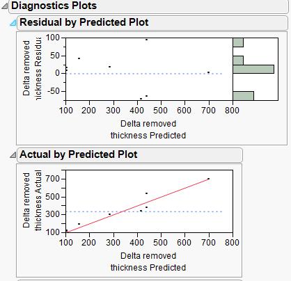
127 112
128 113

129 Durbin-watson test: AutoCorrelation= and Prob(<DW)=0.7333>>0.05, thus the data for the delta removed thicknesses are not shown a problem with autocorrelated. Note: the p-value is for testing positive autocorrelation. If we were performing a two-sided test, the p-value would still be 2( ), which is still not significant 114
130 2. Monitor area function before and after ISE experiments: The Overlay Plot is the comparison of the measured S 2 /P for the fused silica before and after all ISE experiments. When depth was less than 50nm, the differences between the two data sets were pronounced. When depth was over 50nm, the differences between the two data were small and random. There is no statistical test for the results, because there is no replication. 115
131 3. Influences of sample preparation on indentation size effect The overlay plot of the Log 10 (hardness) vs. Depth clearly demonstrates that the hardness curve for the 2 nd electropolished surface overlapped that for the 1 st electropolished surface. The consistent results for electropolished surfaces imply that the 116

132 electropolishing step is reproducible and repeatable. The tiny difference between the results for the electropolished surfaces indicates the variation (or uncertainty) of the results. The result of any polishing step highly depends on the qualities of its former steps. All the data for the ISE measurement are correlated. The following statistical analysis also proves this. 117
 are significantly different from group 2 (30h silica polished, 96 silica polished, 1 st")
133 Durbin-watson test: AutoCorrelation= and Prob(<DW)=0.001<0.05, thus the data for the delta removed thicknesses are highly autocorrelated. Among the 5 data set, group 1(alumina polished, 8h silica polished) are significantly different from group 2 (30h silica polished, 96 silica polished, 1 st electropolished, 2 nd electropolished). 118
Determination of Strain Gradient Plasticity Length Scale for Microelectronics Solder Alloys
 Juan Gomez Universidad EAFIT, Medellin, Colombia Cemal Basaran Electronic Packaging Laboratory, University at Buffalo, State University of New York, 212 Ketter Hall, Buffalo, NY 14260 e-mail: cjb@buffalo.edu
Two opposite size effects of hardness at real nano-scale and their distinct origins
 www.nature.com/scientificreports Received: 21 June 2017 Accepted: 16 October 2017 Published: xx xx xxxx OPEN Two opposite size effects of hardness at real nano-scale and their distinct origins Rong Yang,
Evaluation of length scale effects for micro and nano-sized cantilevered structures
 University of Wollongong Research Online University of Wollongong Thesis Collection 1954-2016 University of Wollongong Thesis Collections 2010 Evaluation of length scale effects for micro and nano-sized
M3 Review Automated Nanoindentation
 M3 Review Automated Nanoindentation Prepared by Duanjie Li, PhD & Pierre Leroux 6 Morgan, Ste156, Irvine CA 92618 P: 949.461.9292 F: 949.461.9232 nanovea.com Today's standard for tomorrow's materials.
YIELD & TENSILE STRENGTH OF STEEL & ALUMINIUM USING MICROINDENTATION
 YIELD & TENSILE STRENGTH OF STEEL & ALUMINIUM USING MICROINDENTATION Prepared by Duanjie Li, PhD & Pierre Leroux 6 Morgan, Ste156, Irvine CA 9618 P: 949.461.99 F: 949.461.93 nanovea.com Today's standard
Review Review of Nanoindentation Size Effect: Experiments and Atomistic Simulation
 Review Review of Nanoindentation Size Effect: Experiments and Atomistic Simulation George Z. Voyiadjis * and Mohammadreza Yaghoobi Computational Solid Mechanics Laboratory, Department of Civil and Environmental
EDGE CHIPPING RESISTANCE USING MACROINDENTATION TESTING
 EDGE CHIPPING RESISTANCE USING MACROINDENTATION TESTING Prepared by Ali Mansouri 6 Morgan, Ste156, Irvine CA 92618 P: 949.461.9292 F: 949.461.9232 nanovea.com Today's standard for tomorrow's materials.
Full Nanomechanical Characterization of Ultra-Thin Films
 APPLICATION NOTE By: Jeffrey Schirer and Julia Nowak, Ph.D. Hysitron, Inc. Eiji Kusano and Mune-aki Sakamoto Department of Chemistry, Kanazawa Institute of Technology, Japan Full Nanomechanical Characterization
Tablet Coating Failure Using Micro Scratch Testing
 Tablet Coating Failure Using Micro Scratch Testing Prepared by Jorge Ramirez 6 Morgan, Ste156, Irvine CA 92618 P: 949.461.9292 F: 949.461.9232 nanovea.com Today's standard for tomorrow's materials. 2011
ME -215 ENGINEERING MATERIALS AND PROCESES
 ME -215 ENGINEERING MATERIALS AND PROCESES Instructor: Office: MEC325, Tel.: 973-642-7455 E-mail: samardzi@njit.edu PROPERTIES OF MATERIALS Chapter 3 Materials Properties STRUCTURE PERFORMANCE PROCESSING
Nanoindentation. Kathy Walsh, Ph.D. Frederick Seitz Materials Research Laboratory University of Illinois at Urbana-Champaign
 Nanoindentation Kathy Walsh, Ph.D. Frederick Seitz Materials Research Laboratory University of Illinois at Urbana-Champaign Mechanical Testing: How does it respond when you poke it, squish it, or stretch
NANOINDENTATION OF SILICON CARBIDE WAFER COATINGS
 NANOINDENTATION OF SILICON CARBIDE WAFER COATINGS Prepared by Jesse Angle 6 Morgan, Ste156, Irvine CA 9618 P: 949.461.99 F: 949.461.93 nanovea.com Today's standard for tomorrow's materials. 010 NANOVEA
Evaluation of Mechanical Properties of Hard Coatings
 Evaluation of Mechanical Properties of Hard Coatings Comprehensive mechanical testing of two coated metal samples was performed on the UNMT- 1. The tests clearly distinguished brittle and ductile samples,
STRENGTHENING MECHANISM IN METALS
 Background Knowledge Yield Strength STRENGTHENING MECHANISM IN METALS Metals yield when dislocations start to move (slip). Yield means permanently change shape. Slip Systems Slip plane: the plane on which
Nanoindentation, Scratch and nanodma : Innovations for Atomic Force Microscopes. Ryan Stromberg
 Nanoindentation, Scratch and nanodma : Innovations for Atomic Force Microscopes Ryan Stromberg 09-07-2017 2 Outline Hysitron TriboScope Technology Mechanical Testing Indenter Stylus vs. AFM Cantilever
Surface effects on nanoindentation
 Surface effects on nanoindentation Tong-Yi Zhang a) and Wei-Hua Xu Department of Mechanical Engineering, Hong Kong University of Science and Technology, Clear Water Bay, Kowloon, Hong Kong, China (Received
3. MECHANICAL PROPERTIES OF STRUCTURAL MATERIALS
 3. MECHANICAL PROPERTIES OF STRUCTURAL MATERIALS Igor Kokcharov 3.1 TENSION TEST The tension test is the most widely used mechanical test. Principal mechanical properties are obtained from the test. There
MICROINDENTATION & FRACTURE OF MINERAL ROCK
 MICROINDENTATION & FRACTURE OF MINERAL ROCK Prepared by Jorge Ramirez 6 Morgan, Ste156, Irvine CA 92618 P: 949.461.9292 F: 949.461.9232 nanovea.com Today s standard for tomorrow s materials. INTRO The
Computer Simulation of Nanoparticle Aggregate Fracture
 Mater. Res. Soc. Symp. Proc. Vol. 1056 2008 Materials Research Society 1056-HH08-45 Computer Simulation of Nanoparticle Aggregate Fracture Takumi Hawa 1,2, Brian Henz 3, and Michael Zachariah 1,2 1 National
Module-6. Dislocations and Strengthening Mechanisms
 Module-6 Dislocations and Strengthening Mechanisms Contents 1) Dislocations & Plastic deformation and Mechanisms of plastic deformation in metals 2) Strengthening mechanisms in metals 3) Recovery, Recrystallization
Chapter Outline Dislocations and Strengthening Mechanisms. Introduction
 Chapter Outline Dislocations and Strengthening Mechanisms What is happening in material during plastic deformation? Dislocations and Plastic Deformation Motion of dislocations in response to stress Slip
Repetition: Adhesion Mechanisms
 Repetition: Adhesion Mechanisms a) Mechanical interlocking b) Monolayer/monolayer c) Chemical bonding d) Diffusion e) Psedo diffusion due to augmented energy input (hyperthermal particles) Repetition:
XPM: High Speed Nanoindentation and Mechanical Property Mapping. Eric Hintsala, Ph.D
 XPM: High Speed Nanoindentation and Mechanical Property Mapping Eric Hintsala, Ph.D. 2017-10-05 2 Table of Contents 1. Introduction: Brief overview of nanoindentation and nanomechanical property mapping
Introduction. Introduction. The micro mechanical properties of the wood cell wall. Xinan Zhang M.S. Candidate
 The micro mechanical properties of the wood cell wall Xinan Zhang M.S. Candidate Nowadays, with the fast development of nanotechnology, more attention has been paid to micro and sub-micro scale area. The
Dynamic Nanoindentation Characterization: nanodma III. Ude Hangen, Ph.D
 Dynamic Nanoindentation Characterization: nanodma III Ude Hangen, Ph.D. 2017-11-02 Displacement 11/02/2017 Bruker Confidential 2 nm mm mm Outline Elastic-Plastic vs. Viscoelastic Materials Response nanodma
Mechanical Properties of Materials
 INTRODUCTION Mechanical Properties of Materials Many materials, when in service, are subjected to forces or loads, it is necessary to know the characteristics of the material and to design the member from
Structural Characterization of Amorphous Silicon
 Structural Characterization of Amorphous Silicon Bianca Haberl A thesis submitted for the degree of Doctor of Philosophy of The Australian National University December 2010 Chapter 5 Mechanical Properties
AML 883 Properties and selection of engineering materials
 AML 883 Properties and selection of engineering materials LECTURE 8. Plasticity M P Gururajan Email: guru.courses@gmail.com Room No. MS 207/A 3 Phone: 1340 Problem Sheet 3 Problems on strength limited
Fundamentals of Plastic Deformation of Metals
 We have finished chapters 1 5 of Callister s book. Now we will discuss chapter 10 of Callister s book Fundamentals of Plastic Deformation of Metals Chapter 10 of Callister s book 1 Elastic Deformation
Mechanical Properties of Metals. Goals of this unit
 Mechanical Properties of Metals Instructor: Joshua U. Otaigbe Iowa State University Goals of this unit Quick survey of important metal systems Detailed coverage of basic mechanical properties, especially
Materials and their structures
 Materials and their structures 2.1 Introduction: The ability of materials to undergo forming by different techniques is dependent on their structure and properties. Behavior of materials depends on their
Finite Element Simulation of the Process of Aluminum. Alloy Resistance Spot Welding
 Finite Element Simulation of the Process of Aluminum Alloy Resistance Spot Welding Li Baoqing, Shan Ping, Lian Jinrui, Hu Shengsun, Cheng Fangjie Tianjin University, Tianjin, P.R.C Abstract In this paper,
Substrate Effect, Pile-Up and Sink-In Factors during Thin Film Nanoindentation. Kevin Russell Schwieker
 Substrate Effect, Pile-Up and Sink-In Factors during Thin Film Nanoindentation by Kevin Russell Schwieker A thesis submitted to the Graduate Faculty of Auburn University in partial fulfillment of the requirements
HARDMEKO 2007 Recent Advancement of Theory and Practice in Hardness Measurement November, 2007, Tsukuba, Japan
 HARDMEKO 7 Recent Advancement of Theory and Practice in Hardness Measurement 9- November, 7, Tsukuba, Japan DIFFERENCES OF PERFORMANCE BETWEEN THE STEEL STANDARD BLOCKS FOR HARDNESS MADE IN JAPAN AND THAT
Direct nano-crystalline Ni plating on titanium surfaces
 Direct nano-crystalline Ni plating on titanium surfaces Dr Mohammad Sakhawat Hussain PhD (Aston) FIMF FIMMM CEng Department of Materials Engineering Faculty of Mechanical Engineering Universiti Teknologi
The influence of aluminium alloy quench sensitivity on the magnitude of heat treatment induced residual stress
 Materials Science Forum Vols. 524-525 (26) pp. 35-31 online at http://www.scientific.net (26) Trans Tech Publications, Switzerland The influence of aluminium alloy quench sensitivity on the magnitude of
Deformation Twinning in Bulk Aluminum with Coarse Grains
 Proceedings of the 12th International Conference on Aluminium Proceedings Alloys, of the September 12th International 5-9, 2010, Yokohama, Conference Japan on 2010 Aluminum The Japan Alloys, Institute
Module 3 Machinability. Version 2 ME IIT, Kharagpur
 Module 3 Machinability Lesson 14 Failure of cutting tools and tool life Instructional objectives At the end of this lesson, the students will be able to (i) (ii) (iii) (iv) (v) State how the cutting tools
Application Note #124 VITA: Quantitative Nanoscale Characterization and Unambiguous Material Identification for Polymers
 Local thermal analysis identifies polymer AFM image of polymer blend Application Note #124 VITA: Quantitative Nanoscale Characterization and Unambiguous Material Identification for Polymers VITA module
Strengthening Mechanisms
 Strengthening Mechanisms The ability of a metal/ alloy to plastically deform depends on the ability of dislocations to move. Strengthening techniques rely on restricting dislocation motion to render a
NANO SCRATCH TESTING OF THIN FILM ON GLASS SUBSTRATE
 NANO SCRATCH TESTING OF THIN FILM ON GLASS SUBSTRATE Prepared by Jesse Angle 6 Morgan, Ste156, Irvine CA 92618 P: 949.461.9292 F: 949.461.9232 nanovea.com Today's standard for tomorrow's materials. 2010
THE NEXT GENERATION OF GERMANIUM SUBSTRATES: EXPOGER
 THE NEXT GENERATION OF GERMANIUM SUBSTRATES: EXPOGER Pieter Arickx (1), Rufi Kurstjens (1), Wim Geens (1), Kristof Dessein (1) (1) Umicore Electro-Optic Materials, Watertorenstraat 33 B2250 Olen (Belgium),
Microindentation Hardness Testing
 MICROINDENTATION HARDNESS TESTING Microindentation hardness testing, more commonly (but incorrectly) called microhardness testing, is widely used to study fine scale changes in hardness, either intentional
INCIPIENT PLASTICITY OF METALS AND ALLOYS USING NANO-INDENTATION TECHNIQUE
 University of Tennessee, Knoxville Trace: Tennessee Research and Creative Exchange Doctoral Dissertations Graduate School 8-2015 INCIPIENT PLASTICITY OF METALS AND ALLOYS USING NANO-INDENTATION TECHNIQUE
Nanoindentation of La-Cr-O Thin Films
 Nanoindentation of La-Cr-O Thin Films Anthony Coratolo1, Nina Orlovskaya1 Christopher Johnson2, Randall Gemmen2 1 Drexel University, Philadelphia, USA 2 National Energy Technology Laboratory, Morgantown,
Periodic Table of the Elements
 XII. ARE THE ELEMENTS DUCTILE OR BRITTLE: A NANOSCALE EVALUATION Periodic Table of the Elements The collection of the elements comprise the fundamental set of constituents, not only for all of nature but
TOPIC 2. STRUCTURE OF MATERIALS III
 Universidad Carlos III de Madrid www.uc3m.es MATERIALS SCIENCE AND ENGINEERING TOPIC 2. STRUCTURE OF MATERIALS III Topic 2.3: Crystalline defects. Solid solutions. 1 PERFECT AND IMPERFECT CRYSTALS Perfect
Tensile/Tension Test Advanced Topics
 CIVE.3110 Engineering Materials Laboratory Fall 2017 Tensile/Tension Test Advanced Topics Tzuyang Yu Associate Professor, Ph.D. Structural Engineering Research Group (SERG) Department of Civil and Environmental
Chapter Outline: Failure
 Chapter Outline: Failure How do Materials Break? Ductile vs. brittle fracture Principles of fracture mechanics Stress concentration Impact fracture testing Fatigue (cyclic stresses) Cyclic stresses, the
Point Defects. Vacancies are the most important form. Vacancies Self-interstitials
 Grain Boundaries 1 Point Defects 2 Point Defects A Point Defect is a crystalline defect associated with one or, at most, several atomic sites. These are defects at a single atom position. Vacancies Self-interstitials
Analysis of AE Signals during Scratch Test on the Coated Paperboard
 Analysis of AE Signals during Scratch Test on the Coated Paperboard Hiroyuki Kishi, Akio Matudoe, Ken Yamashita, Shigeru Nagasawa and Yasushi Fukuzawa Department of Mechanical Engineering, Nagaoka University
Dislocations and Plastic Deformation
 Dislocations and Plastic Deformation Edge and screw are the two fundamental dislocation types. In an edge dislocation, localized lattice distortion exists along the end of an extra half-plane of atoms,
NANO SCRATCH/MAR TESTING OF PAINT ON METAL SUBSTRATE
 NANO SCRATCH/MAR TESTING OF PAINT ON METAL SUBSTRATE Prepared by Susana Cabello 6 Morgan, Ste156, Irvine CA 92618 P: 949.461.9292 F: 949.461.9232 nanovea.com Today's standard for tomorrow's materials.
Study of scale effects on mechanical strength of the AA1050 and AA1085 alloys
 Study of scale effects on mechanical strength of the AA1050 and AA1085 alloys Olivier R. Marques oliviermarques@tecnico.ulisboa.pt Instituto Superior Técnico, Universidade de Lisboa, Portugal Abstract
Hysitron TI 980 TriboIndenter. Innovation with Integrity. Tribology and Mechanical Testing
 Hysitron TI 980 TriboIndenter World s Most Advanced Nanomechanical and Nanotribological Testing Innovation with Integrity Tribology and Mechanical Testing Hysitron TI 980 TriboIndenter Accelerate Nanomechanical
Lectures on: Introduction to and fundamentals of discrete dislocations and dislocation dynamics. Theoretical concepts and computational methods
 Lectures on: Introduction to and fundamentals of discrete dislocations and dislocation dynamics. Theoretical concepts and computational methods Hussein M. Zbib School of Mechanical and Materials Engineering
X. DEFINING YIELD STRESS AND FAILURE STRESS (STRENGTH)
") X. DEFINING YIELD STRESS AND FAILURE STRESS (STRENGTH) One of the most obvious but still most difficult problems in dealing with matters of failure is that of defining the yield stress and the failure
X. DEFINING YIELD STRESS AND FAILURE STRESS (STRENGTH) One of the most obvious but still most difficult problems in dealing with matters of failure is that of defining the yield stress and the failure
Lecture # 11 References:
 Lecture # 11 - Line defects (1-D) / Dislocations - Planer defects (2D) - Volume Defects - Burgers vector - Slip - Slip Systems in FCC crystals - Slip systems in HCP - Slip systems in BCC Dr.Haydar Al-Ethari
Mechanical behavior of crystalline materials - Stress Types and Tensile Behaviour
 Mechanical behavior of crystalline materials - Stress Types and Tensile Behaviour 3.1 Introduction Engineering materials are often found to posses good mechanical properties so then they are suitable for
IN-SITU NONDESTRUCTIVE MEASUREMENTS OF KEY MECHANICAL PROPERTIES OF OIL AND GAS PIPELINES
 PVP-Vol. 429, Residual Stress Measurement and General Nondestructive Evaluation ASME 2001 IN-SITU NONDESTRUCTIVE MEASUREMENTS OF KEY MECHANICAL PROPERTIES OF OIL AND GAS PIPELINES Fahmy M. Haggag Advanced
EFFECT OF LOCAL PLASTIC STRETCH OM TOTAL FATIGUE LIFE EVALUATION
 EFFECT OF LOCAL PLASTIC STRETCH OM TOTAL FATIGUE LIFE EVALUATION Abstract G. S. Wang Aeronautics Division, The Swedish Defence Research Agency SE-17290 Stockholm, Sweden wgs@foi.se This paper shows that
THE MEASUREMENT OF SUBSURFACE RESIDUAL STRESS AND COLD WORK DISTRIBUTIONS IN NICKEL BASE ALLOYS
 THE MEASUREMENT OF SUBSURFACE RESIDUAL STRESS AND COLD WORK DISTRIBUTIONS IN NICKEL BASE ALLOYS Paul S. Prevéy Lambda Research, Inc. ABSTRACT A method of determining the diffraction peak width accurately
Mechanical behavior of crystalline materials- Comprehensive Behaviour
 Mechanical behavior of crystalline materials- Comprehensive Behaviour In the previous lecture we have considered the behavior of engineering materials under uniaxial tensile loading. In this lecture we
Defects and Diffusion
 Defects and Diffusion Goals for the Unit Recognize various imperfections in crystals Point imperfections Impurities Line, surface and bulk imperfections Define various diffusion mechanisms Identify factors
THE VDI-3198 INDENTATION TEST EVALUATION OF A RELIABLE QUALITATIVE CONTROL FOR LAYERED COMPOUNDS
 THE VDI-3198 INDENTATION TEST EVALUATION OF A RELIABLE QUALITATIVE CONTROL FOR LAYERED COMPOUNDS N. Vidakis *, A. Antoniadis *, N. Bilalis** * Technological Educational Institute of Crete, Greece ** Technical
Optimizing Strain Gage Excitation Levels
 Micro-Measurements Strain ages and Instruments Tech Note TN-502 Optimizing Strain age Excitation Levels Introduction A common request in strain gage work is to obtain the recommended value of bridge excitation
Post-CMP Cleaning: Interaction between Particles and Surfaces
 Post-CMP Cleaning: Interaction between Particles and Surfaces J.-G. Park and T.-G. Kim Department of Materials Engineering, Hanyang University, Ansan, 426-791, South Korea E-mail: jgpark@hanyang.ac.kr
Measurement of Residual Stress by X-ray Diffraction
 Measurement of Residual Stress by X-ray Diffraction C-563 Overview Definitions Origin Methods of determination of residual stresses Method of X-ray diffraction (details) References End Stress and Strain
Case Study: Determination of Hardness and Modulus of Thin Films and Coatings by Nanoindentation:- INDICOAT Contract No.
 Case Study: Determination of Hardness and Modulus of Thin Films and Coatings by Nanoindentation:- INDICOAT Contract No. SMT4--CT98-2249 Dr Nigel M. Jennett 10 th November 2011 This presentation was written
Silver Diffusion Bonding and Layer Transfer of Lithium Niobate to Silicon
 Chapter 5 Silver Diffusion Bonding and Layer Transfer of Lithium Niobate to Silicon 5.1 Introduction In this chapter, we discuss a method of metallic bonding between two deposited silver layers. A diffusion
SPDT Effects on Surface Quality & Subsurface Damage in Ceramics
 SPDT Effects on Surface Quality & Subsurface Damage in Ceramics Deepak Ravindra & John Patten (Manufacturing Research Center- Western Michigan University) Jun Qu (Oak Ridge National Laboratory) Presentation
Materials Engineering 272-C Fall 2001, Lectures 9 & 10. Introduction to Mechanical Properties of Metals
 Materials Engineering 272-C Fall 2001, Lectures 9 & 10 Introduction to Mechanical Properties of Metals From an applications standpoint, one of the most important topics within Materials Science & Engineering
A DISLOCATION MODEL FOR THE PLASTIC DEFORMATION OF FCC METALS AN ANALYSIS OF PURE COPPER AND AUSTENITIC STEEL
 A DISLOCATION MODEL FOR THE PLASTIC DEFORMATION OF FCC METALS AN ANALYSIS OF PURE COPPER AND AUSTENITIC STEEL Background In the bcc model for work hardening in single phase materials, see (6), it is assumed
Integration of Materials Knowledge into Design: Challenges and Opportunities. Surya R. Kalidindi. Funding: NSF, AFOSR-MURI, NIST
 Integration of Materials Knowledge into Design: Challenges and Opportunities Surya R. Kalidindi Funding: NSF, AFOSR-MURI, NIST Material Just Chemistry Different forms of carbon exhibit vastly different
3/28/2011. Mechanical Properties of Wood Cell Wall in a Liquid Environment by Nanoindentation. Outline. Introduction
 Mechanical Properties of Wood Cell Wall in a Liquid Environment by Nanoindentation Yujie Meng PhD student Center for Renewable Carbon Department of Forestry, Wildlife and Fisheries, University of Tennessee,
WEEK FOUR. This week, we will Define yield (failure) in metals Learn types of stress- strain curves Define ductility.
 in metals Learn types of stress- strain curves Define ductility.") WEEK FOUR Until now, we Defined stress and strain Established stress-strain relations for an elastic material Learned stress transformation Discussed yield (failure) criteria This week, we will Define
WEEK FOUR Until now, we Defined stress and strain Established stress-strain relations for an elastic material Learned stress transformation Discussed yield (failure) criteria This week, we will Define
DENSIFICATION OF FUSED SILICA BY STRESS OR LASER IRRADIATION
 Glass Tutorial Series: prepared for and produced by the International Material Institute for New Functionality in Glass An NSF sponsored program material herein not for sale Available at www.lehigh.edu/imi
Doctoral School on Engineering Sciences Università Politecnica delle Marche
 Doctoral School on Engineering Sciences Università Politecnica delle Marche Extended summary Nanoindentazione: dalla calibrazione all'applicazione ai materiali metallici massivi e ai rivestimenti Curriculum:
nano-ta TM : Nano Thermal Analysis
 nano-ta TM : Nano Thermal Analysis Application Note #10 Correlation between nanoscale and bulk Thermal Analysis Authors: Dr. Greg Meyers and Dr. Andrew Pastzor Dow Chemical Introduction Thermal methods
An XPS and Atomic Force Microscopy Study of the Micro-Wetting Behavior of Water on Pure Chromium* 1
 Materials Transactions, Vol. 44, No. 3 (2003) pp. 389 to 395 #2003 The Japan Institute of Metals An XPS and Atomic Force Microscopy Study of the Micro-Wetting Behavior of Water on Pure Chromium* 1 Rongguang
Available online at ScienceDirect. Procedia Engineering 79 (2014 )
") Available online at www.sciencedirect.com ScienceDirect Procedia Engineering 79 (2014 ) 212 217 37th National Conference on Theoretical and Applied Mechanics (37th NCTAM 2013) & The 1st International Conference
Available online at www.sciencedirect.com ScienceDirect Procedia Engineering 79 (2014 ) 212 217 37th National Conference on Theoretical and Applied Mechanics (37th NCTAM 2013) & The 1st International Conference
Plastic deformation mechanisms in nanocrystalline columnar grain structures
 Plastic deformation mechanisms in nanocrystalline columnar grain structures Diana Farkas a and William A. Curtin b a Department of Materials Science and Engineering, Virginia Tech, Blacksburg, VA 24061,
What if your diffractometer aligned itself?
 Ultima IV Perhaps the greatest challenge facing X-ray diffractometer users today is how to minimize time and effort spent on reconfiguring of the system for different applications. Wade Adams, Ph.D., Director,
True Stress and True Strain
 True Stress and True Strain For engineering stress ( ) and engineering strain ( ), the original (gauge) dimensions of specimen are employed. However, length and cross-sectional area change in plastic region.
RESIDUAL STRESSES IN SHOT PEENED COMPONENTS by David Kirk
 RESIDUAL STRESSES IN SHOT PEENED COMPONENTS by David Kirk INTRODUCTION Shot peening of components produces a magic skin containing compressive residual macrostress. This skin has a thickness that is largely
Creep Rates and Stress Relaxation for Micro-sized Lead-free Solder Joints
 Creep Rates and Stress Relaxation for Micro-sized Lead-free Solder Joints Summary This Note describes a new method for the measurement of some materials properties of lead-free solders, in particular the
MECHANICAL AND PHYSICAL PROPRIETIES
 Kera-Coat Ceramic Coatings are Special Ceramic Coating defined as a substantially vitreous or glassy inorganic coating bonded to metal by fusion at a temperature above 800 F. In this short abstract we
MECHANICAL PROPERTIES
 MECHANICAL PROPERTIES Mechanical Properties: In the course of operation or use, all the articles and structures are subjected to the action of external forces, which create stresses that inevitably cause
ELECTRICAL RESISTIVITY AS A FUNCTION OF TEMPERATURE
 ELECTRICAL RESISTIVITY AS A FUNCTION OF TEMPERATURE Introduction The ability of materials to conduct electric charge gives us the means to invent an amazing array of electrical and electronic devices,
GLOBAL RATCHETING BY ELASTIC-PLASTIC FEA ACCORDING TO ASME SECTION VIII RULES
 Proceedings of the ASME 2011 Pressure Vessels & Piping Division Conference Proceedings of PVP2011 2011 ASME Pressure July Vessels 17-21, and 2011, Piping Baltimore, Division Maryland, Conference USA July
ENGN2340 Final Project Computational rate independent Single Crystal Plasticity with finite deformations Abaqus Umat Implementation
 ENGN2340 Final Project Computational rate independent Single Crystal Plasticity with finite deformations Abaqus Umat Implementation Anastasia Tzoumaka Fall 2017 Intorduction: Single crystals, are monocrystalline
PLASTIC DEFORMATION AND THE ONSET OF TENSILE INSTABILITY
 PLASTIC DEFORMATION AND THE ONSET OF TENSILE INSTABILITY Introduction In this experiment the plastic deformation behavior and the onset of plastic instability of some common structural alloys is investigated.
CB x 33 x 70 cm
 MECHANICAL TESTERS The Mechanical Tester has been designed with leading edge technologies in order to give the highest accuracy and repeatability on the widest range of measurements. This focus on quality
Application Note #1007 All-Inclusive Scratch Testing of Coatings and Thin Films Using Bruker's Universal Test System
 Scratch with ECR Scratch with E UMT TriboLab pplication Note #1007 ll-inclusive Scratch Testing of Coatings and Thin Films Using ruker's Universal Test System Coatings and thin films are being used increasingly
AFM Probe-Based Data Recording Technology
 AFM Probe-Based Data Recording Technology Prof. Bharat Bhushan bhushan.2@osu.eduh Nanoprobe Laboratory for Bio- & Nanotechnology and Biomimetics Nanoprobe Laboratory for Bio- & Nanotechnology and Biomimetics
Earth & Planetary Science Applications of X-Ray Diffraction: Advances Available for Research with our New Systems
 Earth & Planetary Science Applications of X-Ray Diffraction: Advances Available for Research with our New Systems James R. Connolly Dept. of Earth & Planetary Sciences University of New Mexico 401/501
Carbon nanostructures. (http://www.mf.mpg.de/de/abteilungen/schuetz/index.php?lang=en&content=researchtopics&type=specific&name=h2storage)
") Carbon nanostructures (http://www.mf.mpg.de/de/abteilungen/schuetz/index.php?lang=en&content=researchtopics&type=specific&name=h2storage) 1 Crystal Structures Crystalline Material: atoms arrange into a
Carbon nanostructures (http://www.mf.mpg.de/de/abteilungen/schuetz/index.php?lang=en&content=researchtopics&type=specific&name=h2storage) 1 Crystal Structures Crystalline Material: atoms arrange into a
Mechanical Properties
 Mechanical Properties Elastic deformation Plastic deformation Fracture II. Stable Plastic Deformation S s y For a typical ductile metal: I. Elastic deformation II. Stable plastic deformation III. Unstable
Analysis of Shear Wall Transfer Beam Structure LEI KA HOU
 Analysis of Shear Wall Transfer Beam Structure by LEI KA HOU Final Year Project report submitted in partial fulfillment of the requirement of the Degree of Bachelor of Science in Civil Engineering 2013-2014