This document is downloaded from DR-NTU, Nanyang Technological University Library, Singapore.
|
|
|
- Randell Ramsey
- 5 years ago
- Views:
Transcription
1 This document is downloaded from DR-NTU, Nanyang Technological University Library, Singapore. Title Author(s) Citation Effect of Ni P thickness on solid-state interfacial reactions between Sn 3.5Ag solder and electroless Ni P metallization on Cu substrate Kumar, Aditya; Chen, Zhong; Mhaisalkar, Subodh Gautam; Wong, Chee Cheong; Teo, Poi Siong; Kripesh, Vaidhyanathan Kumar, A., Chen, Z., Mhaisalkar, S. G., Wong, C. C., Teo, P. S., & Kripesh, V. (2005). Effect of Ni P thickness on solid-state interfacial reactions between Sn 3.5Ag solder and electroless Ni P metallization on Cu substrate. Thin Solid Films, 504(1-2), Date 2005 URL Rights 2005 Elsevier B.V. This is the author created version of a work that has been peer reviewed and accepted for publication by Thin Solid Films, Elsevier B.V. It incorporates referee s comments but changes resulting from the publishing process, such as copyediting, structural formatting, may not be reflected in this document. The published version is available at: [
2 Effect of Ni P thickness on solid-state interfacial reactions between Sn 3.5Ag solder and electroless Ni P metallization on Cu substrate Aditya Kumar a,*, Zhong Chen a, S.G. Mhaisalkar a, C.C. Wong a, Poi Siong Teo b, Vaidhyanathan Kripesh b a School of Materials Science and Engineering, Nanyang Technological University, Nanyang Avenue, Singapore , Singapore b Institute of Microelectronics, 11 Science Park Road, Singapore , Singapore * Corresponding author. Tel.: ; fax: address: aditya@pmail.ntu.edu.sg (A. Kumar). Abstract Solid-state interfacial reactions between Sn 3.5Ag solder and electroless Ni P metallization on Cu substrate were investigated for three different Ni P thicknesses. It was found that during interfacial reactions, Ni 3 Sn 4 intermetallic grows at the Sn 3.5Ag/Ni P interface along with the crystallization of electroless Ni P layer into Ni 3 P compound. Additional interfacial compounds (IFCs) such as Ni Sn P, Cu 3 Sn, Cu 6 Sn 5, (Ni 1-x Cu x ) 3 Sn 4, and (Ni 1-x Cu x ) 6 Sn 5 were also found to grow at the Sn 3.5Ag/Ni P/Cu interfaces depending upon the Ni--P thickness. In the sample with thin Ni P layer, formation of these IFCs appeared at lower aging temperature and within shorter aging duration than in the samples with thicker Ni P. The complete dissolution of electroless Ni P layer into Ni 3 P and Ni Sn P layers was found to be the main cause for the growth of additional IFCs. Across the Ni 3 P and Ni Sn P layers, diffusion of Cu and Sn takes place resulting in the formation of Cu Sn and Ni Cu Sn intermetallics. It is shown in
3 this paper that multi-layered IFC growth at the Sn 3.5Ag/Ni P/Cu interfaces can be avoided by the selection of proper Ni P thickness. Keywords: Electroless nickel; Solder; Interfacial reaction; Intermetallic compound 1. Introduction Under bump metallization (UBM) is a combination of thin metallic layers which not only provides good solderable surface but also protects the underlying IC metallization from reacting with solder. During soldering process, UBM reacts with solder and forms a thin layer of interfacial compound (IFC). Formation of the thin layer is desirable to achieve good metallurgical bond. However, excess growth of the IFC affects the mechanical reliability of the solder joint which is a generic reliability problem in flip-chip solder joints [1 3]. Cu is a promising UBM material for Sn Pb solder because of its good wettability with solder. However, Cu reacts rapidly with Sn of the solder forming thick layers of Cu Sn intermetallics. This IFC over-growth problem is exacerbated in the case of Pb-free solders, used due to the legislation and environmental concerns, as the Pb-free solders are Sn-rich alloys constituting one or two more elements such as Ag, Cu, and Bi. The IFC growth has been found to be reduced in the case of Ni UBM, as the reaction between Ni and Sn is much slower than between Cu and Sn [4]. The Ni UBM can be deposited by various chemical and physical deposition techniques. Among them, electroless nickel with a thin layer of immersion gold has been considered as a promising UBM due to its easy processing and low cost. Electroless nickel is a Ni P alloy, where P comes from hypophosphite-reducing agent during the reduction of Ni from an ionic Ni solution. The presence of P in the electroless Ni P UBM causes its complicated interfacial reactions with solder. The interfacial reactions include formation of Ni 3 Sn 4 intermetallic and Ni 3 P compound at the solder/ni P interface [2 12]. Other reaction products such as Ni 3 Sn 2 and Ni 12 P 5 were also reported [5,7], although Ni 3 Sn 4 and Ni 3 P were the major phases. Further, a ternary Ni Sn P
4 compound was also reported to form at the solder/ni P interface [8], which grew during liquid-state aging [9,10]. Recently, it was found [12] that this Ni Sn P compound can grow even during solid-state aging. Although numerous studies have been done on the interfacial reactions between solder and electroless Ni P UBM, the understanding made so far on the influence of Ni P UBM thickness on the interfacial reactions is incomplete. Accordingly, in this work, solid-state interfacial reactions between solder and electroless Ni P UBM on Cu substrate were studied for different thicknesses of Ni P UBM. 2. Experimental procedure Cu (99.99%) plate of size of 70 mm 25 mm 6 mm was used to fabricate the multilayered reaction samples Cu/Ni P/ Sn 3.5Ag/Ni P/Cu. The Cu plate was surface cleaned, first by polishing down to 1 μm finish, then by ultrasonically cleaning with acetone for 10 min, then by etching with 20 vol.% HNO 3 solution for a few seconds, and finally by cleaning with deionized water. Electroless Ni P was plated on the surface cleaned Cu plate in two steps. In the first step, Cu surface was activated using the ruthenium-based commercial pre-initiator. Then, electroless Ni P was plated on the activated Cu surface using commercial electroless nickel solution. Electroless Ni P metallization, of three different thicknesses, was plated on the Cu plate by selecting the three different deposition times but at the same process conditions. Thin layer (~500 Å ) of non-cyanide immersion gold was also deposited on the electroless Ni P surface to protect the surface from oxidation. The electroless Ni P coated Cu plate was cut into two pieces of size of 40 mm 25 mm 6 mm and 30 mm 25 mm 6 mm, and then joined with each other using Sn 3.5Ag solder. Fig. 1 illustrates the set-up used to join the plates. The joint was formed during the reflow process by placing a number of small pieces of solder wires on the small electroless Ni P coated Cu plate and pressing them by the big plate. No-clean paste flux was applied on both the plates before placing the Sn 3.5Ag wires. The reflow process was carried out in IR reflow oven (ESSEMTEC RO-06E) which involved preheating at 150 C for 100 sec, then reflowing at 250 C for 60 sec, and finally cooling down to 160 C in the oven. Alumina spacers of thickness of around 650 μm were used to
5 maintain the uniform thickness of solder in between the plates. The joined plates were cut into a number of small samples with the help of diamond saw. Fig. 2 shows the schematic diagram of reaction sample. As-prepared reaction samples were isothermally aged in the oven (Lenton WHT4/30) at 160, 180, and 200 C for 48, 100, 225, and 400 h. After aging, the samples were removed from the oven and cooled in air to room temperature. JEOL JSM6360A scanning electron microscope (SEM) was used for microstructure analysis. For the crosssectional SEM, the samples were cold mounted in epoxy and polished down to 1 μm finish. After polishing, solder etching was carried out to reveal the microstructure. Etching was done with 4 vol.% hydrochloric acid for a few seconds. Energy dispersive X-ray (EDX) spectroscopy was performed in the SEM to analyze the chemical composition of IFCs. 3. Results The thicknesses of three as-plated electroless Ni P layers were measured to be around 3.9, 7.3, and 9.9 μm while the P content was found to be around 16 at.%. According to their thicknesses, the electroless Ni P layers are termed as thin, medium, and thick Ni P As-prepared reaction samples Fig. 3 shows the IFCs formed at the Sn 3.5Ag/Ni P interface in the as-prepared samples having electroless Ni P layers of different thicknesses. Regardless of Ni P thickness, all the samples have similar interfacial microstructure and chemistry. Needletype and chunky-type Ni 3 Sn 4 intermetallic formed at the Sn 3.5Ag/Ni P interface during the reflow, some of which spalled off into the molten solder. Underneath the Ni 3 Sn 4, Ni Sn P layer formed whose composition was difficult to measure by EDX in the SEM owing to its submicron thickness. Underneath the Ni Sn P layer, a dark thin Ni 3 P layer having large number of voids formed within the electroless Ni P layer.
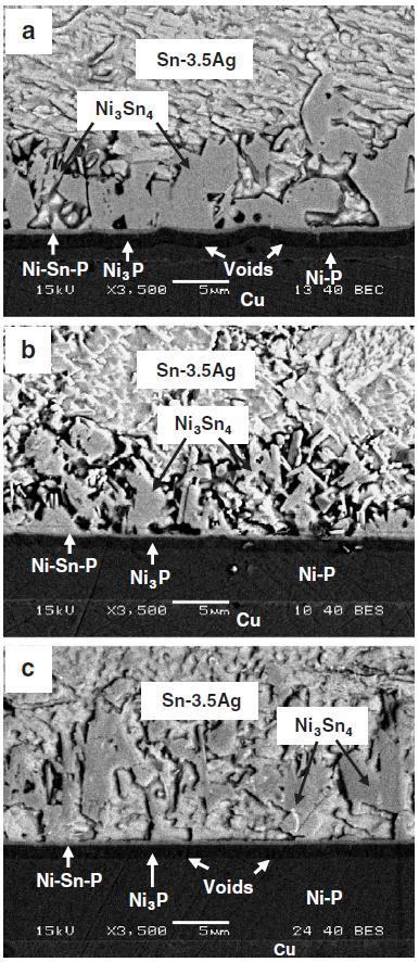
6 3.2. Aged reaction samples Solid-state aging at 150 C for 1000 h is a required reliability test for solder/ubm joint [4]. In this work, solid-state aging was carried out at higher temperatures (160 to 200 C) to shorten the aging duration to 400 h. Fig. 4 shows the back-scattered SEM images of Sn 3.5Ag/Ni P/Cu interfaces in the samples aged at 160 C for 225 h showing the growth of Ni 3 Sn 4 intermetallic and Ni 3 P layer. It can be observed that in the sample with thin Ni P, the electroless Ni P layer completely transformed into Ni 3 P, whereas in other samples, it was still present underneath the Ni 3 P layer. The thickness of this completely transformed electroless Ni P layer (~1.9 μm) is much smaller than that of as-plated electroless Ni P layer (~3.9 μm). This shrinkage in the electroless Ni P layer indicates that during the aging, Ni diffused out from the electroless Ni P layer to form the Ni 3 Sn 4, leaving behind a higher P content Ni P (Ni 3 P) layer within the electroless Ni P layer. It can be observed that in all the samples, several voids formed in the Ni 3 P layer due to the depletion of Ni. However, a layer of voids also formed at the Ni 3 P/Cu interface in the sample with thin Ni P (Fig. 4a). In addition, in this sample, the Ni 3 Sn 4 intermetallic was found to have Cu up to 5 at.%. The presence of Cu in the Ni 3 Sn 4 and formation of layer of voids at the Ni 3 P/Cu interface imply that the Cu diffused out from the Cu substrate to the Ni 3 Sn 4 in the samples with thin Ni P. Fig. 5 shows the back-scattered SEM images of Sn 3.5Ag/Ni P/Cu interfaces in the samples aged at 180 C for 225 h showing the growth of Ni 3 Sn 4, Ni 3 P, Ni Sn P, and Ni Cu Sn IFC layers. From Fig. 5, it is clear that the thickness of electroless Ni P UBM influences the growth of IFCs. Along with the transformation of electroless Ni P into Ni 3 P, only Ni 3 Sn 4 grew predominantly in the sample with thick Ni P, whereas, Ni Sn P also grew in the other samples. This Ni Sn P layer grew at the expense of Ni 3 P layer (Fig. 5a and b). The chemical composition of this Ni Sn P layer was found similar to that of Ni 2 SnP compound. It can be seen that in the sample with thick Ni P, the number of voids formed at the Ni 3 P/Cu interface is negligible as compared to the other samples. In this sample, the Cu content of Ni 3 Sn 4 intermetallic (<1 at.%) was also negligible as compared to the other samples having Cu up to 7 at.%.
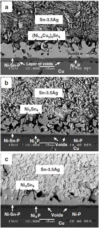
7 Fig. 6 shows the back-scattered SEM images of Sn 3.5Ag/Ni P/Cu interfaces in the samples aged at 200 C for 400 h showing the growth of Ni Cu Sn, Ni Sn P, and Cu Sn IFCs. It can be seen that electroless Ni P layer completely dissolved into Ni Sn P in all the samples. In the sample with thin Ni P, two layers of Cu Sn intermetallics, Cu 6 Sn 5 and Cu 3 Sn, formed at the Ni Sn P/Cu interface. The Cu 3 Sn formed close to Cu substrate, understood to be due to the large availability of Cu from the Cu substrate. In the sample with thin Ni P, two Ni Cu Sn intermetallics of distinct colors, (Ni 1-x Cu x ) 3 Sn 4 and (Ni 1- xcu x ) 6 Sn 5, also formed at the Ni 3 Sn 4 /Ni Sn P interface. On the other hand, no Cu Sn or (Ni 1-x Cu x ) 6 Sn 5 intermetallics were found to form in the samples with medium and thick Ni P, however, (Ni 1-x Cu x ) 3 Sn 4 formed with Cu up to 6 at.%. 4. Discussion 4.1. Growth mechanism of IFCs In this study, it was found that various IFCs such as Ni 3 Sn 4, Ni Sn P, Ni 3 P, Cu Sn, and Ni Cu Sn form during the Sn 3.5Ag/Ni P/Cu interfacial reactions. Although formation of many of these IFCs has been reported in the several studies [2 12], understanding made on their growth mechanism is still not complete. From the present investigation, it is clear that during Sn 3.5Ag/Ni P/Cu interfacial reactions, initially, Sn of solder reacts with electroless Ni P to form Ni 3 Sn 4 and Ni Sn P layer and then Ni 3 Sn 4 intermetallic and Ni 3 P compound grow on the different sides of Ni Sn P layer (Figs. 3 and 4). The dominant growth of Ni 3 Sn 4, over that of Ni Sn P, suggests that Ni 3 Sn 4 might have lower activation energy of formation than that of Ni Sn P. For the growth of Ni 3 Sn 4, Sn comes from the solder to the Ni 3 Sn 4 /Ni Sn P interface [5], where it reacts with Ni that is coming from the electroless Ni P layer. The depletion of Ni from the electroless Ni P layer causes its crystallization or transformation into Ni 3 P compound [6]. During the crystallization, electroless Ni P layer shrinks into columnar grains of Ni 3 P. The shrinkage in electroless Ni P layer, along the direction of growth of IFC layers, is compensated by the growth of Ni 3 Sn 4 layer. Whilst in the perpendicular directions it is compensated by the counter flux of vacancies. These vacancies accumulate and form columnar Kirkendall voids in the Ni 3 P layer.
8 The growth of Ni 3 Sn 4, over that of Ni Sn P, is continued as long as Ni is available from the underlying electroless Ni P layer; otherwise, Sn will react with Ni 3 P layer to form Ni Sn P. The same was observed in the samples aged at 180 C for 225 h and had thin and medium Ni P layers, where electroless Ni P layer completely transformed into Ni 3 P (Fig. 5a and b). Subsequently, in the absence of Ni supply, Sn started reacting with Ni 3 P layer to form Ni Sn P. After complete dissolution of Ni 3 P layer into Ni Sn P, Sn reaches the Cu substrate and forms Cu 3 Sn and Cu 6 Sn 5 intermetallics at the Ni Sn P/Cu interface (Fig. 6a). At the same time, Cu starts diffusing out from the Cu surface to the Ni 3 Sn 4 /Ni Sn P interface and forms (Ni 1-x Cu x ) 3 Sn 4 and (Ni 1-x Cu x ) 6 Sn 5 intermetallics due to the reaction with Ni 3 Sn 4. Initially, the (Ni 1-x Cu x ) 3 Sn 4 intermetallic with low Cu content forms and then eventually the (Ni 1-x Cu x ) 6 Sn 5 intermetallic with high Cu content (Table 1) forms due to the continued supply of Cu. Since during the Sn 3.5Ag/Ni P/Cu interfacial reactions, several IFCs such as Ni Sn P, Cu Sn, and Ni Cu Sn grow only after complete crystallization of electroless Ni P UBM. Thus, the growth of these IFCs can be hindered by preventing the complete crystallization of electroless Ni P UBM and this can be achieved by increasing the Ni P thickness Diffusion of Cu through Ni 3 P layer From the results, it can be observed that Cu diffuses through the Ni 3 P layer (Figs. 4a and 5). However, the mechanism of Cu diffusion has to be understood. Electroless Ni P UBM is a good diffusion barrier due to its amorphous structure. The amorphous structure lacks the grain boundaries and thus inhibits the grain boundary diffusion. The structure of electroless Ni P generally depends upon its P content [13]; amorphous if P is higher than 12.5 at.% and nanocrystalline otherwise. Thus, the as-plated electroless Ni P layer (with 16 at.% P) was amorphous in nature, which transformed into bi-layered Ni P, crystalline Ni 3 P layer on the electroless Ni P layer, during the reflow (Fig. 3). This Ni 3 P layer grew continuously at the expense of electroless Ni P layer during the aging (Figs. 4 and 5). It was found previously [6,11] that the Ni 3 P layer has columnar grains. Therefore, as this
9 layer reached the Cu substrate, Cu started diffusing through the grain boundaries of Ni 3 P layer. A schematic illustration of Cu diffusion through the Ni 3 P layer is shown in Fig. 7. As Sn 3.5Ag/Ni P interfacial reactions proceed, Ni diffuses out from the electroless Ni P layer through the grain boundaries of Ni 3 P layer to form Ni 3 Sn 4 and thus results in the growth of Ni 3 P layer (Fig. 7a). This process is continued until the Ni 3 P layer reaches the Cu substrate; after that, Cu starts diffusing out from the Cu substrate through the grain boundaries of Ni 3 P layer to compensate the Ni supply (Fig. 7b). It is to be understood that as long as electroless Ni P layer is present on the Cu substrate, Cu cannot diffuse out due to the lack of grain boundaries in the electroless Ni P. However, after its crystallization into Ni 3 P, grain boundaries of Ni 3 P layer provide diffusion paths for Cu atoms. Thus, the diffusion of Cu from the Cu substrate can be inhibited by preventing the complete crystallization of electroless Ni P UBM, which directly depends upon the thickness of electroless Ni P UBM. 5. Conclusions In this study, solid-state interfacial reactions between Sn 3.5Ag solder and electroless Ni P UBM on Cu substrate were investigated for three different Ni P thicknesses. The following conclusions were made based on the study 1. Initially, three distinct IFC layers, Ni 3 Sn 4, Ni Sn P, and Ni 3 P, form at the Sn 3.5Ag/Ni P interface during the interfacial reactions. The Ni 3 P layer grows within the electroless Ni P layer due to the depletion of Ni. Columnar voids form in the Ni 3 P layer to compensate the Ni depletion. 2. As the Ni 3 P layer reaches the Cu substrate, Cu starts diffusing out from the Cu substrate through the grain boundaries of Ni 3 P layer and forms Ni Cu Sn intermetallics due to the reaction with Ni 3 Sn 4. In the absence of Ni supply, Sn starts reacting with Ni 3 P layer to form Ni Sn P. After complete dissolution of Ni 3 P layer into Ni Sn P, Sn reaches the Cu substrate and forms Cu Sn intermetallics at the Ni Sn P/Cu interface.
10 3. Thickness of electroless Ni P UBM influences the growth of IFCs at the Sn 3.5Ag/Ni P/Cu interfaces due to the amount of Ni available from the electroless Ni P. In the samples with thin (3.9 μm) Ni P, various IFCs such as Ni Sn P, Cu 3 Sn, Cu 6 Sn 5, (Ni 1-x Cu x ) 3 Sn 4, and (Ni 1-x Cu x ) 6 Sn 5 grew at lower aging temperature and within shorter duration as compared to the samples with thicker (7.3 and 9.9 μm) Ni P. Thus, the growth of these IFCs can be avoided by using the Ni P UBM of proper thickness. Acknowledgements This work was supported by School of Materials Science and Engineering, NTU, and Institute of Microelectronics. Helpful discussion with Dr. Andriy M. Gusak is gratefully acknowledged.
11 References [1] C.Y. Liu, C. Chen, A.K. Mal, K.N. Tu, J. Appl. Phys. 85 (1999) [2] M.O. Alam, Y.C. Chan, K.N. Tu, J. Appl. Phys. 94 (2003) [3] Z. Chen, M. He, A. Kumar, G.J. Qi, J. Electron. Mater., in press. [4] K.N. Tu, K. Zeng, Mater. Sci. Eng., R Rep. 34 (2001) 1. [5] C.Y. Lee, K.L. Lin, Thin Solid Films 249 (1994) 201. [6] J.W. Jang, P.G. Kim, K.N. Tu, D.R. Frear, P. Thompson, J. Appl. Phys. 85 (1999) [7] P.L. Liu, Z. Xu, J.K. Shang, Metall. Mater. Trans., A Phys. Metall. Mater. Sci. 31A (2000) [8] H. Matsuki, H. Ibuka, H. Saka, Sci. Technol. Adv. Mater. 3 (2002) 261. [9] Y.D. Jeon, A. Ostmann, H. Reichl, K.W. Paik, Electron. Compon. Technol. Conf. (IEEE) (2003) [10] S.J. Wang, C.Y. Liu, Scr. Mater. 49 (2003) 813. [11] M. He, Z. Chen, G. Qi, Acta Mater. 52 (2004) [12] A. Kumar, M. He, Z. Chen, Surf. Coat. Technol. 198 (2005) 283. [13] G.O. Mallory, J.B. Hajdu, Electroless Plating: Fundamental and Applications, American Electroplaters and Surface Finishes Society, Orlando, 1990.
12 List of Tables Table 1 EDX results showing the chemical composition (at.%) of IFCs formed at the Sn 3.5Ag/Ni P/Cu interfaces in Fig. 6a
13 List of Figures Fig. 1 Fig. 2 Fig. 3 Fig. 4 Fig. 5 Fig. 6 Fig. 7 Schematic illustration for joining the electroless Ni P coated Cu plates. Schematic diagram of reaction sample. Back-scattered SEM images of Sn 3.5Ag/Ni P/Cu interfaces in the asprepared samples having electroless Ni P layers of thickness of (a) 3.9 μm, (b) 7.3 μm, and (c) 9.9 μm. Back-scattered SEM images of Sn 3.5Ag/Ni P/Cu interfaces in the samples aged at 160 C for 225 hand having (a) thin (3.9 μm), (b) medium (7.3 μm), and (c) thick (9.9 μm) Ni P layers. Back-scattered SEM images of Sn 3.5Ag/Ni P/Cu interfaces in the samples aged at 180 C for 225 h and having (a) thin (3.9 μm), (b) medium (7.3 μm), and (c) thick (9.9 μm) Ni P layers. Back-scattered SEM images of Sn 3.5Ag/Ni P/Cu interfaces in the samples aged at 200 C for 400 hand having (a) thin (3.9 μm), (b) medium (7.3 μm), and (c) thick (9.9 μm) Ni P layers. Schematic illustration of Cu diffusion through the Ni 3 P layer: (a) growth of Ni 3 P layer in between Ni 3 Sn 4 intermetallic and electroless Ni P layer; (b) diffusing of Cu through the grain boundaries of Ni 3 P layer.
14 Table 1
15 Fig. 1
16 Fig. 2
17 Fig. 3
18 Fig. 4
19 Fig. 6
20 Fig. 7
This document is downloaded from DR-NTU, Nanyang Technological University Library, Singapore.
 This document is downloaded from DR-NTU, Nanyang Technological University Library, Singapore. Title Author(s) Citation Effect of post-reflow cooling rate on intermetallic compound formation between Sn
Interface Reaction Between Electroless Ni Sn P Metallization and Lead-Free Sn 3.5Ag Solder with Suppressed Ni 3 P Formation
 Journal of ELECTRONIC MATERIALS, Vol. 43, No. 11, 2014 DOI: 10.1007/s11664-014-3306-z Ó 2014 The Minerals, Metals & Materials Society Interface Reaction Between Electroless Ni Sn P Metallization and Lead-Free
Dissolution of electroless Ni metallization by lead-free solder alloys
 Journal of Alloys and Compounds 388 (2005) 75 82 Dissolution of electroless Ni metallization by lead-free solder alloys Ahmed Sharif, Y.C. Chan, M.N. Islam, M.J. Rizvi Department of Electronic Engineering,
Metallurgical reaction and mechanical strength of electroless Ni-P solder joints for advanced packaging applications
 JOURNAL OF MATERIALS SCIENCE: MATERIALS IN ELECTRONICS 11 (2000) 587±593 Metallurgical reaction and mechanical strength of electroless Ni-P solder joints for advanced packaging applications K. C. HUNG,
Reaction of Sn-Bearing Solders with Nickel-based Under Bump Metallisations
 STR/03/069/ST Reaction of Sn-Bearing Solders with Nickel-based Under Bump Metallisations G. Qi, M. He and Z. Chen Abstract This work relates to wafer bumping technologies for flip chip packaging applications
A study aimed at characterizing the interfacial structure in a tin silver solder on nickel-coated copper plate during aging
 Sādhanā Vol. 33, Part 3, June 2008, pp. 251 259. Printed in India A study aimed at characterizing the interfacial structure in a tin silver solder on nickel-coated copper plate during aging D C LIN 1,
SIDE WALL WETTING INDUCED VOID FORMATION DUE TO SMALL SOLDER VOLUME IN MICROBUMPS OF Ni/SnAg/Ni UPON REFLOW
 SIDE WALL WETTING INDUCED VOID FORMATION DUE TO SMALL SOLDER VOLUME IN MICROBUMPS OF Ni/SnAg/Ni UPON REFLOW Y. C. Liang 1, C. Chen 1, *, and K. N. Tu 2 1 Department of Materials Science and Engineering,
Comparative study of the dissolution kinetics of electrolytic Ni and electroless Ni P by the molten Sn3.5Ag0.5Cu solder alloy
 Microelectronics Reliability 43 (2003) 2031 2037 www.elsevier.com/locate/microrel Comparative study of the dissolution kinetics of electrolytic Ni and electroless Ni P by the molten Sn3.5Ag0.5Cu solder
Effect of 9 wt.% in addition to Sn3.5Ag0.5Cu solder on the interfacial reaction with the Au/NiP metallization on Cu pads
 Journal of Alloys and Compounds 396 (2005) 217 223 Effect of 9 wt.% in addition to Sn3.5Ag0.5Cu solder on the interfacial reaction with the Au/NiP metallization on Cu pads M.N. Islam, Y.C. Chan, A. Sharif,
Intermetallic Reactions in a Sn-20In-2.8Ag Solder Ball-Grid-Array Package with Au/Ni/Cu Pads
 Journal of ELECTRONIC MATERIALS, Vol. 34, No. 11, 2005 Regular Issue Paper Intermetallic Reactions in a Sn-20In-2.8Ag Solder Ball-Grid-Array Package with Au/Ni/Cu Pads HUI-MIN WU, 1,2 FENG-CHIH WU, 1 and
Effect of indium addition in Sn-rich solder on the dissolution of Cu metallization
 Journal of Alloys and Compounds 390 (2005) 67 73 Effect of indium addition in Sn-rich solder on the dissolution of Cu metallization Ahmed Sharif, Y.C. Chan Department of Electronic Engineering, City University
Effect of Ni-P Plating Temperature on Growth of Interfacial Intermetallic Compound in Electroless Nickel Immersion Gold/Sn-Ag-Cu Solder Joints
 Journal of ELECTRONIC MATERIALS, Vol. 47, No. 1, 2018 DOI: 10.1007/s11664-017-5821-1 Ó 2017 The Minerals, Metals & Materials Society Effect of Ni-P Plating Temperature on Growth of Interfacial Intermetallic
Interfacial Reactions between the Sn-9Zn Solder and Au/Ni/SUS304 Multi-layer Substrate
 , July 6-8, 2011, London, U.K. Interfacial Reactions between the Sn-9Zn Solder and Au/Ni/SUS304 Multi-layer Substrate *Yee-Wen Yen 1, Chien-Chung Jao 2, Kuo-Sing Chao 1, Shu-Mei Fu Abstract Sn-9Zn lead-free
Mechanical Reliability of Aged Lead- Free Solders
 Report number: Mechanical Reliability of Aged Lead- Free Solders Susanne Lewin 2012 Dept. of Material Science and Engineering Royal Institute of Technology Stockholm, Sweden Dept. of Material Science and
Controlling the Microstructures from the Gold-Tin Reaction
 Controlling the Microstructures from the Gold-Tin Reaction J. Y. Tsai, C. W. Chang, Y. C. Shieh, Y. C. Hu, and C. R. Kao* Department of Chemical & Materials Engineering National Central University Chungli
Undercooling, Microstructures and Hardness of Sn-Rich Pb-Free Solders on Cu-xZn Alloy Under Bump Metallurgies
 Materials Transactions, Vol. 50, No. 9 (2009) pp. 2291 to 2296 #2009 The Japan Institute of Metals Undercooling, Microstructures and Hardness of Sn-Rich Pb-Free Solders -xzn Alloy Under Bump Metallurgies
Growth of Intermetallic Compounds during Isothermal Annealing of a Sn-Ag-Cu Lead-free Solder
 Accepted for publication in Soldering & Surface Mount Technology, Emerald, United Kingdom, 2004, in press. Growth of Intermetallic Compounds during Isothermal Annealing of a Sn-Ag-Cu Lead-free Solder S.L.
Intermetallic Compounds Formed in Sn-20In-2.8Ag Solder BGA Packages with Ag/Cu Pads C.C. Jain, S.S. Wang, K.W. Huang, and T.H.
 JMEPEG ÓASM International DOI: 10.1007/s11665-008-9292-7 1059-9495/$19.00 Intermetallic Compounds Formed in Sn-20In-2.8Ag Solder BGA Packages with Ag/Cu Pads C.C. Jain, S.S. Wang, K.W. Huang, and T.H.
Supplementary Materials for
 www.sciencemag.org/cgi/content/full/336/6084/1007/dc1 Supplementary Materials for Unidirectional Growth of Microbumps on (111)-Oriented and Nanotwinned Copper Hsiang-Yao Hsiao, Chien-Min Liu, Han-wen Lin,
Interfacial reactions of Sn Cu solder with Ni/Au surface finish on Cu pad during reflow and aging in ball grid array packages
 Materials Science and Engineering B 117 (2005) 246 253 Interfacial reactions of Sn Cu solder with Ni/Au surface finish on Cu pad during reflow and aging in ball grid array packages M.N. Islam, Y.C. Chan
Interfacial reactions of BGA Sn 3.5%Ag 0.5%Cu and Sn 3.5%Ag solders during high-temperature aging with Ni/Au metallization
 Materials Science and Engineering B 113 (2004) 184 189 Interfacial reactions of BGA Sn 3.5%Ag 0.5%Cu and Sn 3.5%Ag solders during high-temperature aging with Ni/Au metallization Ahmed Sharif, M.N. Islam,
Mean-time-to-failure study of flip chip solder joints on CuÕNi V ÕAl thin-film under-bump-metallization
 JOURNAL OF APPLIED PHYSICS VOLUME 94, NUMBER 9 1 NOVEMBER 2003 Mean-time-to-failure study of flip chip solder joints on CuÕNi V ÕAl thin-film under-bump-metallization W. J. Choi, a) E. C. C. Yeh, b) and
HIGH-DENSITY interconnection technology requires
 IEEE TRANSACTIONS ON COMPONENTS AND PACKAGING TECHNOLOGIES, VOL. 31, NO. 2, JUNE 2008 431 Effect of 0.5 wt% Cu in Sn-3.5%Ag Solder to Retard Interfacial Reactions With the Electroless Ni-P Metallization
Yasunori Chonan 1,2,, Takao Komiyama 1, Jin Onuki 1, Ryoichi Urao 2, Takashi Kimura 3 and Takahiro Nagano Introduction
 Materials Transactions, Vol. 43, No. 8 (2002) pp. 1840 to 1846 Special Issue on Lead-Free Electronics Packaging c 2002 The Japan Institute of Metals Influence of Phosphorus Concentration in Electroless
Electroless Ni-W-P alloys as barrier coatings for liquid solder interconnects
 Loughborough University Institutional Repository Electroless Ni-- alloys as barrier coatings for liquid solder interconnects This item was submitted to Loughborough University's Institutional Repository
Interfacial reactions of Sn Cu and Sn Pb Ag solder with Au/Ni during extended time reflow in ball grid array packages
 Interfacial reactions of Sn Cu and Sn Pb Ag solder with Au/Ni during extended time reflow in ball grid array packages M.N. Islam, Y.C. Chan, a) and A. Sharif Department of Electronic Engineering, City
Thermal cyclic test for Sn-4Ag-0.5Cu solders on high P Ni/Au and Ni/Pd/Au surface finishes
 Journal of Mechanical Engineering and Sciences (JMES) ISSN (Print): 2289-4659; e-issn: 2231-8380; Volume 9, pp. 1572-1579, December 2015 Universiti Malaysia Pahang, Malaysia DOI: http://dx.doi.org/10.15282/jmes.9.2015.4.0152
Ball shear strength and fracture mode of lead-free solder joints prepared using nickel nanoparticle doped flux
 Ball shear strength and fracture mode of lead-free solder joints prepared using nickel nanoparticle doped flux G. K. Sujan a, A. S. M. A. Haseeb a, *, Chong Hoe Jian b, Amalina Afifi a a Department of
Lead-Free Solder Bump Technologies for Flip-Chip Packaging Applications
 Lead-Free Solder Bump Technologies for Flip-Chip Packaging Applications Zaheed S. Karim 1 and Jim Martin 2 1 Advanced Interconnect Technology Ltd. 1901 Sunley Centre, 9 Wing Yin Street, Tsuen Wan, Hong
Wetting Properties of and Interfacial Reactions in Lead-free Sn-Zn Based Solders on Cu and Cu Plated with an Electroless Ni-P/Au Layer
 Materials Transactions, Vol. 45, No. 2 (2004) pp. 588 to 594 #2004 The Japan Institute of Metals EXPRESS REGULAR ARTICLE Wetting Properties of and Interfacial Reactions in Lead-free Sn-Zn Based Solders
Comparative Study of NiNiP Leadframes from Different Processes
 Comparative Study of NiNiP Leadframes from Different Processes Wu-Hu Li *1, Jeffrey Khai Huat Low 1, Harry Sax 2, Raymond Solis Cabral 1, Esperidion De Castro Salazar 1, Pauline Min Wee Low 1 1 Infineon
Thermomigration and electromigration in Sn58Bi ball grid array solder joints
 J Mater Sci: Mater Electron (2010) 21:1090 1098 DOI 10.1007/s10854-009-9992-2 Thermomigration and electromigration in Sn58Bi ball grid array solder joints X. Gu K. C. Yung Y. C. Chan Received: 18 August
Intermetallic Compounds Formed during the Reflow and Aging of Sn-3.8Ag-0.7Cu and Sn-20In-2Ag-0.5Cu Solder Ball Grid Array Packages
 Journal of ELECTRONIC MATERIALS, Vol. 33, No. 3, 2004 Regular Issue Paper Intermetallic Compounds Formed during the Reflow and Aging of Sn-3.8Ag-0.7Cu and Sn-20In-2Ag-0.5Cu Solder Ball Grid Array Packages
Effect of Surface Finishes on Ball Shear Strength in BGA Joints with Sn 3.5 mass%ag Solder
 Materials Transactions, Vol. 43, No. 4 (2002) pp. 751 to 756 c 2002 The Japan Institute of Metals EXPRESS REGULR RTICLE Effect of Surface Finishes on all Shear Strength in G Joints with Sn 3.5 mass%g Solder
Shear Strength in Solder Bump Joints for High Reliability Photodiode Packages
 Materials Transactions, Vol. 44, No. 10 (2003) pp. 2163 to 2168 #2003 The Japan Institute of Metals Shear Strength in Solder Bump Joints for High Reliability Photodiode Packages Chong-Hee Yu 1, Kyung-Seob
Effect of Process Variations on Solder Joint Reliability for Nickel-based Surface Finishes
 Effect of Process Variations on Solder Joint Reliability for Nickel-based Surface Finishes Hugh Roberts Atotech USA Inc., Rock Hill, SC, USA Sven Lamprecht, Gustavo Ramos and Christian Sebald Atotech Deutschland
Research Paper. Isothermal solidification bonding of Bi2Te2.55Se0.45 thermoelectric material with Cu electrodes
 Engineering & Technology Research 3(3): 000-000, February 2019 DOI: 10.15413/etr.2019.0001 2019 Academia Publishing Research Paper Isothermal solidification bonding of Bi2Te2.55Se0.45 thermoelectric material
Effects of Minor Fe, Co, and Ni Additions on the Reaction Between SnAgCu Solder and Cu
 Effects of Minor Fe, Co, and Ni Additions on the Reaction Between SnAgCu Solder and Cu Y. W. Wang, C. R. Kao* Department of Materials Science and Engineering National Taiwan University Taipei 106, Taiwan
Intermetallic Reactions in Sn-3.5Ag Solder Ball Grid Array Packages with Ag/Cu and Au/Ni/Cu Pads
 Journal of ELECTRONIC MATERIALS, Vol. 35, No. 3, 2006 Regular Issue Paper Intermetallic Reactions in Sn-3.5Ag Solder Ball Grid Array Packages with Ag/Cu and Au/Ni/Cu Pads CHIH-CHIEN CHI 1 and TUNG-HAN
The Effect of Cu and Ni on the Structure and Properties of the IMC Formed by the Reaction of Liquid Sn-Cu Based Solders with Cu Substrate
 WDS'08 Proceedings of Contributed Papers, Part III, 220 224, 2008. ISBN 978-80-7378-067-8 MATFYZPRESS The Effect of Cu and Ni on the Structure and Properties of the IMC Formed by the Reaction of Liquid
This article appeared in a journal published by Elsevier. The attached copy is furnished to the author for internal non-commercial research and
 This article appeared in a journal published by Elsevier. The attached copy is furnished to the author for internal non-commercial research and education use, including for instruction at the authors institution
Effect of Ni or Co Addition to Sn-Ag Solder on Microstructure and Joint Strength at Interface
 Materials Transactions, Vol. 49, No. 7 (28) pp. 1518 to 1523 Special Issue on Lead-Free Soldering in Electronics IV #28 The Japan Institute of Metals Effect of Ni or Co Addition to Sn-Ag Solder on Microstructure
EFFECT OF THERMAL AGING ON THE IMC LAYER BETWEEN SnAgSb SOLDER AND Cu SUBSTRATE. Universiti Kebangsaan Malaysia, 43600, Bangi, Selangor, Malaysia
 EFFECT OF THERMAL AGING ON THE IMC LAYER BETWEEN SnAgSb SOLDER AND Cu SUBSTRATE W. Shualdi 1, I. Ahmad 1, G. Omar 2 and A. Isnin 3 1 Department of Electrical, Electronic and System, Faculty of Engineering,
IBM Research Report. Yoon-Chul Sohn, Jin Yu KAIST 373-1, Guseong-Dong, Yuseong-Gu Daejeon Korea
 RC23513 (W0502-039) February 4, 2005 Materials Science IBM Research Report Effect of Intermetallics Spalling on the Mechanical Behavior of Electroless Ni(P)/Pb-free Solder Interconnection Yoon-Chul Sohn,
Flip Chip Bump Formation of Sn 1.8Bi 0.8Cu 0.6In Solder by Stencil Printing
 Materials Transactions, Vol. 46, No. 11 (2005) pp. 2359 to 2365 Special Issue on Lead-Free Soldering in Electronics III #2005 The Japan Institute of Metals Flip Chip Bump Formation of Sn 1.8Bi 0.8Cu 0.6In
Kyoung-Soon Bok, Woo-Suk Choi, and Chul-Lae Cho Samsung Techwin co., LTD. 14 Nongseo-Ri, Kiheung-Eub, Youngin-Si, Kyoungki-Do, , Korea
 Studies on Ni-Sn Intermetallic Compound and P-rich Ni Layer at the ckel UBM - Solder Interface and Their Effects on Flip Chip Solder Joint Reliability Young-Doo Jeon and Kyung-Wook Paik Micro-Electronic
Inhibition of Electromigration in Eutectic SnBi Solder Interconnect by Plastic Prestraining
 J. Mater. Sci. Technol., 2011, 27(11), 1072-1076. Inhibition of Electromigration in Eutectic SnBi Solder Interconnect by Plastic Prestraining X.F. Zhang 1), H.Y. Liu 1), J.D. Guo 1) and J.K. Shang 1,2)
Growth Kinetics of Reaction Layers in Flip Chip Joints with Cu-cored Lead-free Solder Balls
 Materials Transactions, Vol. 5, No. 3 () pp. 75 to 75 Special Issue on Lead-Free Soldering in Electronics # The Japan Institute of Metals Growth Kinetics of Reaction Layers in Flip Chip Joints with Cu-cored
Electromigration failure mechanisms for SnAg3.5 solder bumps on Ti/Cr-Cu/Cu and Ni P /Au metallization pads
 JOURNAL OF APPLIED PHYSICS VOLUME 96, NUMBER 8 15 OCTOBER 2004 Electromigration failure mechanisms for SnAg3.5 solder bumps on Ti/Cr-Cu/Cu and Ni P /Au metallization pads T. L. Shao, Y. H. Chen, S. H.
Effect of Bath Life of Ni(P) on the Brittle-Fracture Behavior of Sn-3.0Ag-0.5Cu/ENIG
 on the Brittle-Fracture Behavior of Sn-3.0Ag-0.5Cu/ENIG") Journal of ELECTRONIC MATERIALS, Vol. 43, No. 12, 2014 DOI: 10.1007/s11664-014-3395-8 Ó 2014 The Minerals, Metals & Materials Society Effect of Bath Life of Ni(P) on the Brittle-Fracture Behavior of Sn-3.0Ag-0.5Cu/ENIG
Journal of ELECTRONIC MATERIALS, Vol. 43, No. 12, 2014 DOI: 10.1007/s11664-014-3395-8 Ó 2014 The Minerals, Metals & Materials Society Effect of Bath Life of Ni(P) on the Brittle-Fracture Behavior of Sn-3.0Ag-0.5Cu/ENIG
The Effect of Fillers in Nonconductive Adhesive on the Reliability of Chip-on-Glass Bonding with Sn/Cu Bumps
 Materials Transactions, Vol. 52, No. 11 (2011) pp. 2106 to 2110 #2011 The Japan Institute of Metals The Effect of Fillers in Nonconductive Adhesive on the Reliability of Chip-on-Glass Bonding with Sn/Cu
Electromigration Behavior of through-si-via (TSV) Interconnect for 3-D Flip Chip Packaging
 Interconnect for 3-D Flip Chip Packaging") Materials Transactions, Vol. 51, No. 5 (2010) pp. 1020 to 1027 #2010 The Japan Institute of Metals EXPRESS REGULAR ARTICLE Electromigration Behavior of through-si-via (TSV) Interconnect for 3-D Flip Chip
Materials Transactions, Vol. 51, No. 5 (2010) pp. 1020 to 1027 #2010 The Japan Institute of Metals EXPRESS REGULAR ARTICLE Electromigration Behavior of through-si-via (TSV) Interconnect for 3-D Flip Chip
Influence of Thermal Cycling on the Microstructure and Shear Strength of Sn3.5Ag0.75Cu and Sn63Pb37 Solder Joints on Au/Ni Metallization
 68 J. Mater. Sci. Technol., Vol.23 No.1, 2007 Influence of Thermal Cycling on the Microstructure and Shear Strength of Sn3.5Ag0.75Cu and Sn63Pb37 Solder Joints on Au/Ni Metallization Hongtao CHEN 1,2),
Interfacial Reactions between Ni-Zn Alloy Films and Lead-free Solders
 Interfacial Reactions between -Zn Alloy Films and Lead-free Solders Pay Ying Chia 1, A.S.M.A. Haseeb 2 University of Malaya Department of Mechanical Engineering, University of Malaya, 50603, Kuala Lumpur,
Effect of pinhole Au/Ni/Cu substrate on self-alignment of advanced packages
 Materials Science and Engineering B76 (2000) 87 94 www.elsevier.com/locate/mseb Effect of pinhole Au/Ni/Cu substrate on self-alignment of advanced packages K.C. Hung, Y.C. Chan *, H.C. Ong, P.L. Tu, C.W.
This document is downloaded from DR-NTU, Nanyang Technological University Library, Singapore.
 This document is downloaded from DR-NTU, Nanyang Technological University Library, Singapore. Title Effect of Ni-coated carbon nanotubes on interfacial intermetallic layer growth Author(s) Citation Han,
Bi Layer Formation at the Anode Interface in Cu/Sn 58Bi/Cu Solder Joints with High Current Density
 J. Mater. Sci. Technol., 2012, 28(1), 46 52. Bi Layer Formation at the Anode Interface in Cu/Sn 58Bi/Cu Solder Joints with High Current Density Hongwen He 1), Haiyan Zhao 1), Fu Guo 2) and Guangchen Xu
Electric current effect on microstructure of ball grid array solder joint
 Journal of Alloys and Compounds 392 (2005) 237 246 Electric current effect on microstructure of ball grid array solder joint B.Y. Wu, Y.C. Chan Department of Electronic Engineering, City University of
Improving mechanical and electrical properties of Cu/SAC305/Cu solder joints under electromigration by using Ni nanoparticles doped flux
 https://doi.org/10.1007/s10854-017-8252-0 Improving mechanical and electrical properties of Cu/SAC305/Cu solder joints under electromigration by using Ni nanoparticles doped flux M. Nasir Bashir 1 A. S.
Future Electronic Devices Technology in Cosmic Space and Electroless Ni/Pd/Au Plating for High Density Semiconductor Package Substrate
 JAXA 25 rd Microelectronics Workshop Future Electronic Devices Technology in Cosmic Space and Electroless Ni/Pd/Au Plating for High Density Semiconductor Package Substrate November 2, 2012 Yoshinori Ejiri
The Morphology Evolution and Voiding of Solder Joints on QFN Central Pads with a Ni/Au Finish
 The Morphology Evolution and Voiding of Solder Joints on QFN Central Pads with a Ni/Au Finish Julie Silk 1, Jianbiao Pan 2, Mike Powers 1 1 Agilent Technologies, 1400 Fountaingrove Parkway, Santa Rosa,
Study of Interfacial Reactions Between Sn(Cu) Solders and Ni-Co Alloy Layers
 Solders and Ni-Co Alloy Layers") Journal of ELECTRONIC MATERIALS, Vol. 39, No. 11, 2010 DOI: 10.1007/s11664-010-1346-6 Ó 2010 TMS Study of Interfacial Reactions Between Sn(Cu) Solders and Ni-Co Alloy Layers K.C. HUANG, 1 F.S. SHIEU, 1
Journal of ELECTRONIC MATERIALS, Vol. 39, No. 11, 2010 DOI: 10.1007/s11664-010-1346-6 Ó 2010 TMS Study of Interfacial Reactions Between Sn(Cu) Solders and Ni-Co Alloy Layers K.C. HUANG, 1 F.S. SHIEU, 1
Effect of Iron Plating Conditions on Reaction in Molten Lead-Free Solder
 Materials Transactions, Vol. 45, No. 3 (24) pp. 741 to 746 Special Issue on Lead-Free Soldering in Electronics #24 The Japan Institute of Metals Effect of Iron Plating Conditions on Reaction in Molten
Sn-RICH PHASE COARSENING DURING ISOTHERMAL ANNEALING ON Sn-Ag-Cu SOLDER. N. Saud and A. Jalar
 International Journal of Mechanical and Materials Engineering (IJMME), Vol. 4 (2009), No. 2, 147-151 Sn-RICH PHASE COARSENING DURING ISOTHERMAL ANNEALING ON Sn-Ag-Cu SOLDER. N. Saud and A. Jalar School
Effect of Rare Earth Elements on Lead Free Solder Alloys
 RESEARCH ARTICLE OPEN ACCESS Effect of Rare Earth Elements on Lead Free Solder Alloys Prerna Mishra*, S.N. Alam**, Rajnish Kumar*** * (Department of Metallurgical & Materials Engineering, NIT Rourkela,
Growth mechanism of Ni 3 Sn 4 in a Sn/Ni liquid/solid interfacial reaction
 Available online at www.sciencedirect.com Acta Materialia 57 (2009) 5196 5206 www.elsevier.com/locate/actamat Growth mechanism of Ni 3 Sn 4 in a Sn/Ni liquid/solid interfacial reaction J. Shen a, Y.C.
IBM Research Report. Undercooling and Microhardness of Pb-free Solders on Various UBMs
 RC24583 (W0806-041) June 11, 2008 Materials Science IBM Research Report Undercooling and Microhardness of Pb-free Solders on Various UBMs Moon Gi Cho 1, Sung K. Kang 2, Hyuck Mo Lee 1 * 1 Department of
SCIENCE & TECHNOLOGY
 Pertanika J. Sci. & Technol. 25 (4): 1249-1254 (2017) SCIENCE & TECHNOLOGY Journal homepage: http://www.pertanika.upm.edu.my/ Intermetallic Growth of SAC237 Solder Paste Reinforced with MWCNT Azmah Hanim,
Effect of Magnesium Addition on Microstructure and Mechanical Properties of Lead-Free Zinc-Silver Solder Alloys
 Effect of Magnesium Addition on Microstructure and Mechanical Properties of Lead-Free Zinc-Silver Solder Alloys Md. Anisul Islam * and Ahmed Sharif Department of Materials and Metallurgical Engineering,
Copyright 2008 Year IEEE. Reprinted from IEEE ECTC May 2008, Florida USA.. This material is posted here with permission of the IEEE.
 Copyright 8 Year IEEE. Reprinted from IEEE ECTC 8. 7 - May 8, Florida USA.. This material is posted here with permission of the IEEE. Such permission of the IEEE does not in any way imply IEEE endorsement
Correlations between IMC thickness and three factors in Sn-3Ag-0.5Cu alloy system
 Correlations between IMC thickness and three factors in Sn-3Ag-0.5Cu alloy system MENG Gong-ge( 孟工戈 ) 1, T. Takemoto 2, H. Nishikawa 2 1. College of Materials Science and Engineering, Harbin University
Reflow Profiling: Time a bove Liquidus
 Reflow Profiling: Time a bove Liquidus AIM/David Suraski Despite much research and discussion on the subject of reflow profiling, many questions and a good deal of confusion still exist. What is clear
Comprehensive study of intermetallic compounds in solar cell interconnections and their growth kinetics
 Comprehensive study of intermetallic compounds in solar cell interconnections and their growth kinetics T. Geipel, M. Moeller, A. Kraft, U. Eitner Fraunhofer Institute for Solar Energy Systems ISE 6 th
Effect of Alloying Element on Microstructure and Mechanical Properties of Sn-0.7cu Solder
 International Journal of Current Science, Engineering & Technology Original Research Article Open Access AMCT 2017 Malaysia Special Issue ISSN : 2581-4311 Effect of Alloying Element on Microstructure and
Effect of Ni and Ag on Interfacial Reaction and Microstructure of Sn-Ag-Cu-Ni-Ge Lead-Free Solder
 Reprinted with permission of Materials Science & Technology 2006 Conference and Exhibition Proceedings Effect of Ni and Ag on Interfacial Reaction and Microstructure of Sn-Ag-Cu-Ni-Ge Lead-Free Solder
EFFECT OF ANNEALING AND NICKEL UNDERPLATE ON SUPPRESSION OF TIN WHISKERS
 The 5 th PSU-UNS International Conference on Engineering and 679 Technology (ICET-2011), Phuket, May 2-3, 2011 Prince of Songkla University, Faculty of Engineering Hat Yai, Songkhla, Thailand 90112 EFFECT
Study of the Interface Microstructure of Sn-Ag-Cu Lead-Free Solders and the Effect of Solder Volume on Intermetallic Layer Formation.
 Study of the Interface Microstructure of Sn-Ag-Cu Lead-Free Solders and the Effect of Solder Volume on Intermetallic Layer Formation. B. Salam +, N. N. Ekere, D. Rajkumar Electronics Manufacturing Engineering
Mechanical Properties and Microstructure of Pure Copper Joints Brazed with Amorphous Cu68.5Ni15.7Sn9.3P6.5 Filler Metal
 Mechanical Properties and Microstructure of Pure Copper Joints Brazed with Amorphous Cu68.5Ni15.7Sn9.3P6.5 Filler Metal Jing Zhang 1,*, Weiyuan Yu 2, Wenjiang Lu 2 1 School of Physics and Mechanical-Electrical
Microelectronics Reliability
 Microelectronics Reliability 53 (2013) 899 905 Contents lists available at SciVerse ScienceDirect Microelectronics Reliability journal homepage: www.elsevier.com/locate/microrel Ex situ observations of
Recrystallization of Sn Grains due to Thermal Strain in Sn-1.2Ag-0.5Cu-0.05Ni Solder
 Materials Transactions, Vol. 45, No. 4 (2004) pp. 1383 to 1390 #2004 The Japan Institute of Metals EXPRESS REGULAR ARTICLE Recrystallization of Sn Grains due to Thermal Strain in Sn-1.2Ag-0.5Cu-0.05Ni
Amorphous Si/Au wafer bonding P. H. Chen 1, C. L. Lin 1 and C. Y. Liu 1,2. National Central University, Jhong-Li, Taiwan, R. O. C.
 Amorphous Si/Au wafer bonding P. H. Chen 1, C. L. Lin 1 and C. Y. Liu 1,2 1 Dept. of Chemical Engineering and Materials Engineering, 2 Institute of Materials Science and Engineering, Abstract: National
Micro-Impact Test on Lead-Free BGA Balls on Au/Electrolytic Ni/Cu Bond Pad
 Micro- Test on Lead-Free BGA Balls on Au/Electrolytic Ni/Cu Bond Pad Shengquan Ou*, Yuhuan Xu and K. N. Tu Department of Materials Science and Engineering, UCLA, Los Angeles, CA, 90095-1595 M. O. Alam,
Ceramic Processing Research
 Journal of Ceramic Processing Research. Vol. 11, No. 1, pp. 100~106 (2010) J O U R N A L O F Ceramic Processing Research Factors affecting surface roughness of Al 2 O 3 films deposited on Cu substrates
Suppression of Cu 3 Sn and Kirkendall voids at Cu/Sn-3.5Ag solder joints by adding a small amount of Ge
 J Mater Sci: Mater Electron (2012) 23:56 60 DOI 10.1007/s10854-011-0412-z Suppression of Cu 3 Sn and Kirkendall voids at Cu/Sn-3.5Ag solder joints by adding a small amount of Ge Chun Yu Yang Yang Peilin
EFFECTS OF THERMAL AGING ON INTERMETALLIC COMPOUNDS AND VOIDS FORMATION IN AuAl WIRE BONDING. A. Jalar, M. F. Rosle and M. A. A.
 EFFECTS OF THERMAL AGING ON INTERMETALLIC COMPOUNDS AND VOIDS FORMATION IN AuAl WIRE BONDING A. Jalar, M. F. Rosle and M. A. A. Hamid School of Applied Physics, Faculty of Science and Technology, Universiti
Multi-layered electroless Ni P coatings on powdersintered Nd Fe B permanent magnet. Chen, Zhong; Ng, Alice; Yi, Jianzhang; Chen, Xingfu
 Title Multi-layered electroless Ni P coatings on powdersintered Nd Fe B permanent magnet Author(s) Chen, Zhong; Ng, Alice; Yi, Jianzhang; Chen, Xingfu Citation Chen, Z., Ng, A., Yi, J., & Chen, X. (2006).
Microelectronic Engineering
 Microelectronic Engineering 86 (2009) 2347 2353 Contents lists available at ScienceDirect Microelectronic Engineering journal homepage: www.elsevier.com/locate/mee Effect of small Sn 3.5Ag 0.5Cu additions
Effects of Pd Addition on Au Stud Bumps/Al Pads Interfacial Reactions and Bond Reliability
 Journal of ELECTRONIC MATERIALS, Vol. 33, No. 10, 2004 Special Issue Paper Effects of Pd Addition on Au Stud Bumps/Al Pads Interfacial Reactions and Bond Reliability HYOUNG-JOON KIM, 1,3 JONG-SOO CHO,
PLEASE SCROLL DOWN FOR ARTICLE. Full terms and conditions of use:
 This article was downloaded by: [CAS Chinese Academy of Sciences] On: 6 June 2011 Access details: Access Details: [subscription number 929413865] Publisher Taylor & Francis Informa Ltd Registered in England
1 Thin-film applications to microelectronic technology
 1 Thin-film applications to microelectronic technology 1.1 Introduction Layered thin-film structures are used in microelectronic, opto-electronic, flat panel display, and electronic packaging technologies.
Aging Treatment Characteristics of Shear Strength in Micro Solder Bump
 Materials Transactions, Vol. 43, No. 2 (22) pp. 3234 to 3238 c 22 The Japan Institute of Metals Aging Treatment Characteristics of Shear Strength in Micro Solder Bump Chong-Hee Yu, Kyung-Seob Kim 2, Yong-Bin
Faculty of Mechanical and Manufacturing Engineering, Universiti Tun Hussein Onn Malaysia, Johor, Malaysia
 ', Advanced Materials Research Vol. 845 (2014) pp 76-80 Online available since 2013/Dec/04 at www.scient$c net O (2014) Trans Tech Publications, Switzerland doi: l0.4028/www.scient~~$c. net/amr. 845.76
Effect of Reflow Profile (RSP Vs RTP) on Sn/Ag/Cu Solder Joint Strength in Electronic Packaging
 on Sn/Ag/Cu Solder Joint Strength in Electronic Packaging") ISSN 2231-8798 2012 UniKLBMI Effect of Reflow Profile (RSP Vs RTP) on Sn/Ag/Cu Solder Joint Strength in Electronic Packaging I. Ahmad 1, A. Jalar 2 Z. Kornain 3 & U. Hashim 4 1 Universiti Tenaga Nasional
ISSN 2231-8798 2012 UniKLBMI Effect of Reflow Profile (RSP Vs RTP) on Sn/Ag/Cu Solder Joint Strength in Electronic Packaging I. Ahmad 1, A. Jalar 2 Z. Kornain 3 & U. Hashim 4 1 Universiti Tenaga Nasional
Short Communication Effects of ph on the Immersion Gold Process from a Sulfite- Thiosulfate Solution Based on the Electroless Ni-P Alloy Substrate
 Int. J. Electrochem. Sci., 10 (2015) 7811-7817 International Journal of ELECTROCHEMICAL SCIENCE www.electrochemsci.org Short Communication Effects of ph on the Immersion Gold Process from a Sulfite- Thiosulfate
Effect of the Formation of CuO Flowers and SnO 2 on the Growth of Tin Whiskers on Immersion Tin Surface Finish
 WVCARMEA 2014 ID-119 Effect of the Formation of CuO Flowers and SnO 2 on the Growth of Tin Whiskers on Immersion Tin Surface Finish @ WVCARMEA 2014 22-26 th SEPT 2014 Tin surface 2 Outlines 1. Introduction
Microtexture measurement of copper damascene line with EBSD
 Material Science Forum Vols. 408-412(2002) pp. 529-534 2002 Trans Tech Publications, Switzerland Microtexture measurement of copper damascene line with EBSD Dong-Ik Kim 1*, Jong-Min Paik 1, Young-Chang
Fast Spreading of Liquid SnPb Solder on Gold-coated Copper Wheel Pattern
 J. Mater. Sci. Technol., 2010, 26(12), 1143-1147. Fast Spreading of Liquid SnPb Solder on Gold-coated Copper Wheel Pattern Wei Liu 1), Lei Zhang 1), K.J. Hsia 2) and J.K. Shang 1,3) 1) Shenyang National
Properties of low melting point Sn Zn Bi solders
 Journal of Alloys and Compounds 397 (2005) 260 264 Properties of low melting point Sn Zn Bi solders Jian Zhou, Yangshan Sun, Feng Xue Department of Material Science and Engineering, Southeast University,
EFFECT OF THE MICROSTRUCTURE OF Ni/Au METALLIZATION ON BONDABILITY OF FR-4 SUBSTRATE
 EFFECT OF THE MICROSTRUCTURE OF Ni/Au METALLIZATION ON BONDABILITY OF FR-4 SUBSTRATE Zonghe Lai and Johan Liu The Swedish Institute of Production Engineering Research (IVF) S-431 53 Mölndal, Sweden ABSTRACT
Accumulation (%) Amount (%) Particle Size 0.1
 Amount (%) Particle Size 0.1") 100 10 Amount (%) 5 50 Accumulation (%) 0 0.1 1 Particle Size (µm) 10 0 Supplementary Figure 1. The particle size distribution of W-15 at% Cr after 20 hours milling. Supplementary Figure 2. a,b, X-ray
100 10 Amount (%) 5 50 Accumulation (%) 0 0.1 1 Particle Size (µm) 10 0 Supplementary Figure 1. The particle size distribution of W-15 at% Cr after 20 hours milling. Supplementary Figure 2. a,b, X-ray