Lead-Free Solder Bump Technologies for Flip-Chip Packaging Applications
|
|
|
- Katrina Warren
- 6 years ago
- Views:
Transcription
1 Lead-Free Solder Bump Technologies for Flip-Chip Packaging Applications Zaheed S. Karim 1 and Jim Martin 2 1 Advanced Interconnect Technology Ltd Sunley Centre, 9 Wing Yin Street, Tsuen Wan, Hong Kong Tel: (852) , Fax: (852) , zsk@ait.com.hk 2 Shipley LLC 455 Forest Street, Marlborough, MA 01752, USA Tel: (516) , Fax: (516) , jmartin@shipley.com Abstract We describe the fabrication and characterization of five different types of lead-free solder bump interconnections for use in flip-chip electronic packaging applications. Lead-free solder bumps were fabricated from pure-tin (Sn), tin-bismuth (Sn:Bi), eutectic tin-copper (Sn:Cu), eutectic tin-silver (Sn:Ag), and ternary tinsilver-copper (Sn:Ag:Cu) alloys. The fabrication process consists of the electrolytic plating, using a fountain (cup) plater, of a 5 µm thick copper under-bump-metal (UBM) onto which is plated the lead-free solder. The as-plated bumps were subsequently re-flowed in a 5-zone re-flow oven. Due to the characteristic high-tin compositions of the lead-free solder alloys, which can cause the rapid and uneven formation of tin-copper intermetallics at the bump-ubm interface upon reflow, a unique proprietary nickel cap using a single photolithography process that completely encapsulates the copper UBM was developed. Two different test structures, one with perimeter- and a second with area-distributed solder bumps, each with bumps of average size 125 µm diameter (post-re-flow) were fabricated onto daisy-chain wafers to characterize the lead-free solder bumping and bonding process and to conduct a series of reliability tests. Tests conducted to characterize the properties of the lead-free bumps included Scanning Electron Microscopy (SEM), Energy Dispersive X-ray (EDX), Auger Electron Spectroscopy (AES), micro-sectioning, and ball shear measurements for which the bumps were re-flowed multiple times and subjected to ball shear tests in-between reflows to study the formation of intermetallic compounds. Lead-free solder bumped daisy-chain test die were also flip-chip bonded onto BT-epoxy substrates with patterned copper traces overplated with nickel/gold. The bonded die were underfilled and subjected to environmental tests consisting high-temperature storage, thermal cycling, and accelerated aging. Details of the lead-free solder bump fabrication process together with the performance results including their electrical, mechanical, and reliability characteristics will be presented for all five lead-free alloys chosen in this study. Key words: lead-free, solder bumps, flip-chip, under-bump-metal Introduction Restrictions on the use of lead-containing solders in electronic products are currently under consideration because it is believed that the lead from such products, which are typically disposed of in landfills, have the potential to leach out and contaminate the drinking water system. The electronics industry has been targeted to go lead-free despite the fact that less than 0.5% of all the lead produced annually in the world is used for electronic solders [1]. Laws banning the use of lead in electronics products are due to be enacted in the European Community in January 2008 and similar legislation to restrict the use of lead is pending in both the United States and in Japan [2]. Efforts to identify suitable lead-free finishes for electronic components has thus far been focused mainly on printed circuit boards, leadframe packages, and in the selection of solder pastes. Little attention has being paid to the fabrication of lead-free bump
2 interconnections which are required when packaging integrated circuits (ICs) by flip-chip bonding despite industry predictions that approximately 2.5% of all ICs manufactured in the year 2004 will have to be bumped and packaged using flip-chip [3]. Five different types of lead-free alloy bump materials, with tin constituting a major fraction of the solder, were selected as possible lead-free replacements on the basis of: i) worldwide resources and availability of tin; ii) the comparable cost of the lead-free alloys to lead-tin solder; iii) the bumps can be fabricated using conventional low-cost electroplating techniques; iv) the compatibility of tin-based solders with current re-flow processes, materials, and surface mount equipment, and; v) the familiarity of the electronics manufacturing and assembly industry in handling tin alloys. Tinbismuth bumps with a composition of 90wt%Sn:10wt%Bi and a melting point (MP) of 200 C were fabricated as a potential replacement for eutectic lead-tin solder bumps which have a MP of 183 C. Lead-free bumps made of pure-tin with a MP of 232 C, eutectic tin-copper with a composition of 99.3wt%Sn:0.7wt%Cu with a MP of 227 C, and tinsilver with a eutectic composition of 96.5wt%Sn:3.5wt%Ag and a MP of 221 C were fabrcated as lead-free replacements for both eutectic and high melting point high-lead solder bumps. Ternary composition tin-silver-copper bumps with an alloy composition of 95.8wt%Sn:3.5wt%Ag:0.7wt%Cu and a MP of 216 C were also fabricated by electroplating using a unique process of sequential plating from two separate binary Sn:Cu and Sn:Ag plating solutions. Lead-Free Solder Bump Fabrication Process Lead-free bumps of average size 125 µm in diameter (post-re-flow) were plated onto silicon wafers patterned with perimeter- and area-distributed daisychain test structures (Figs. 1 and 2). Primary steps used in the fabrication of the lead-free bumps consisted of: a) A sputter cleaning step to remove the naturally formed oxide layer on the aluminum bond pads followed by sputter deposition of chrome (thickness of 500 Å) and copper (thickness of 5,000 Å). These two sputtered metals effectively form the adhesion, barrier to indiffusion, and electrical buss layers for plating. b) Patterning of the wafer with an 80 µm thick positive-tone liquid photoresist, positive chrome photomask, UV exposure (using a mask aligner), and developing the thick photoresist to define the areas to be plated. c) Mounting of the wafer in a cup plater and application of current (using contacts at the edges of the wafer) to the underlying copper layer for plating of a 5 µm thick copper under-bump-metal (UBM) layer which acts as a "wettable" foundation to the lead-free solder bump upon re-flow. d) Electroplating of lead-free solder bumps using the appropriate plating solution, anodes, and direct current (DC) or pulse-plating in a fountain (cup) plater system. e) Removal of the thick photoresist and chemical etching of the sputtered copper and chrome layers. f) Application of flux and re-flow of the as-plated bumps in a 5-zone re-flow oven to form the characteristic spherical solder bump shape. Experimental Results Difficulties encountered in the fabrication of the lead-free solder bumps consisted mainly in the control and measurement of the copper composition in the eutectic tin-copper plating bath and the plated deposit since the target value for the copper concentration was only 0.7%. Control of the copper concentration was achieved by continuosly adjusting and measuring the copper in the plating bath solution (provided by Shipley) and the plated deposit and by using pulse plating instead of direct current. Plating solutions were analysed for their copper content using Atomic Absorption Spectroscopy (AAS). Measurement of the composition in the plated deposit was achieved by using Auger Electron Spectroscopy (AES) on crosssectioned re-flowed bumps. Additional techniques such as Differential Scanning Calorimetry (DSC) were also used to determine the melting point and the concentration of the copper in the bumps. Similar methods were used to control and measure the composition of the silver in the tin-silver plating bath (from Shipley) to achieve a eutectic tin-silver bump with approximately 3.5% silver. Accurate control of the percentage of the copper and silver in the eutectic tin-copper and tin-silver bumps is critical due to the rapid change in the melting point of alloys with only a small increase (~1%) in the composition of these two elements. Examples of the as-plated and post re-flowed lead-free pure-tin, tin-bismuth, eutectic tin-copper, eutectic tin-silver, and tin-silver-copper bumps using the fabrication process steps described previously are shown in Scanning Electron Micrographs in Figs. 3-7 respectively. For the ternary tin-silver-copper bumps the fabrication process consisted of a unique method of sequentially plating tin-silver followed by tin-copper (Fig. 7a) and re-flowing the bump to completely mix
3 the solders. This was made possible in part due to the relatively close melting points of the tin-copper and tin-silver alloys. Due to the higher melting point values for the lead-free pure-tin, tin-copper, tin-silver, and tin-silvercopper bumps, the peak re-flow temperatures used were between 250 C to 265 C. During the fabrication and characterization of the lead-free solder bumps Scanning Electron Microscopy (SEM) and Scanning Auger Miroscopy (SAM) measurements on cross-sections of re-flowed tin-silver (3.5% silver) bumps indicated the rapid and uneven formation of tin-copper intermetallics at the interface between the copper UBM and the tin-rich lead-free solder bumps (Figs. 8a - 8d) [4]. This phenomenon was also observed in SAM analyses of the cross-sections of all the other lead-free solder bumps. In order to limit the excessive formation of the tincopper intermetallic compound which is brittle and prone to failure particularly when the layer is too thick, a unique process which completely encapsulates the copper UBM using a single mask step was developed. SAM analysis on a nickel capped copper UBM indicates the effectiveness of this method (Figs. 9a 9d). The advantage of using nickel is its relatively low dissolution rate in tin at [2] 250 C compared to copper (~0.02 microinches per second for nickel compared to ~5.3 microinches per second for copper). All five lead-free solder bumps were subjected to ball shear tests after single and multiple re-flows (JESD22-B117). Preliminary results after single (1X) re-flow show average shear values in excess of 2.5 grams/mil 2 (Table 1) for 100 µm diameter solder balls with all breakages occurring within the bulk of the solders and not at the solder to copper UBM interface. The sample size for the 1X re-flow test was 40 bumps for each solder type. Cross-sections of the bumps showed no detectable voids in the as-plated or post-reflowed bumps and there was no formation of any tincopper intermetallic due to the use of the nickel cap. Lead-free bumped perimeter and area-array daisychain test die were also flip-chip bonded onto BTepoxy substrates, underfilled, and subjected to die shear and environmental tests to determine their suitability for flip-chip-on-board and flip-chip-inpackage applications. Environmental tests consist of high-temperature storage (+150 C for 1,000 hours - JESD22-A103-A), thermal cycling (-40 C to +125 C for 1,000 cycles, 1 cycle/hour, 15 minutes dwell and 15 minutes ramp - JESD22-A104-A Level G), and accelerated aging (100% RH, 15 psig, +121 C for 96 hours - JESD22-A102-B Level C). Tests are on-going and results on the reliability studies will be presented at the conference. Conclusions We have demonstrated the successful fabrication of five different types of lead-free solder bumps consisting of pure-tin, tin-bismuth, tin-copper, tin-silver, and tin-silver-copper. The method of fabrication for all lead-free alloys was by electroplating using a plated copper under-bump-metal. Results indicate that the application of a suitable barrier diffusion layer such as nickel is necessary to limit the excessive formation of tin-copper intermetallic compounds. Preliminary bump shear results have shown that all the lead-free bumps chosen in this study may be suitable replacements for eutectic and highlead solders for use in various flip-chip electronic packaging applications. References [1] Ning-Cheng Lee, Lead-Free Soldering Where the World is Going, Advancing Microelectronics, September/October 1999, pp , [2] Greg Jones, A Period of Adjustment: The Effect of Lead-Free Assembly on the Seminsiductor Iidustry, Chip Scale Review, March/April 2000, pp. 48o TD 0 Tc Tc (-) Scal316 Tw3plated copp35
 each of size 100 µm diameter on a 250 µm pitch.")
4 Fig. 1. Perimeter-distributed daisy-chain test structure with total 36 bumps each of size 150 µm diameter on a 350 µm pitch. Fig. 2. Area-distributed daisy-chain test structure with total 400 bumps (array of 20 x 20) each of size 100 µm diameter on a 250 µm pitch. Average Value (grams) SD (grams) Min Value (grams) Max Value (grams) Shear Height (microns) Sn:(37%)Pb Pure Sn Sn:(10%)Bi Sn:(0.8%)Cu Sn:(3.5%)Ag Table 1: Bump shear values after 1X re-flow on lead-free solder bumps of average size 100 microns diameter.


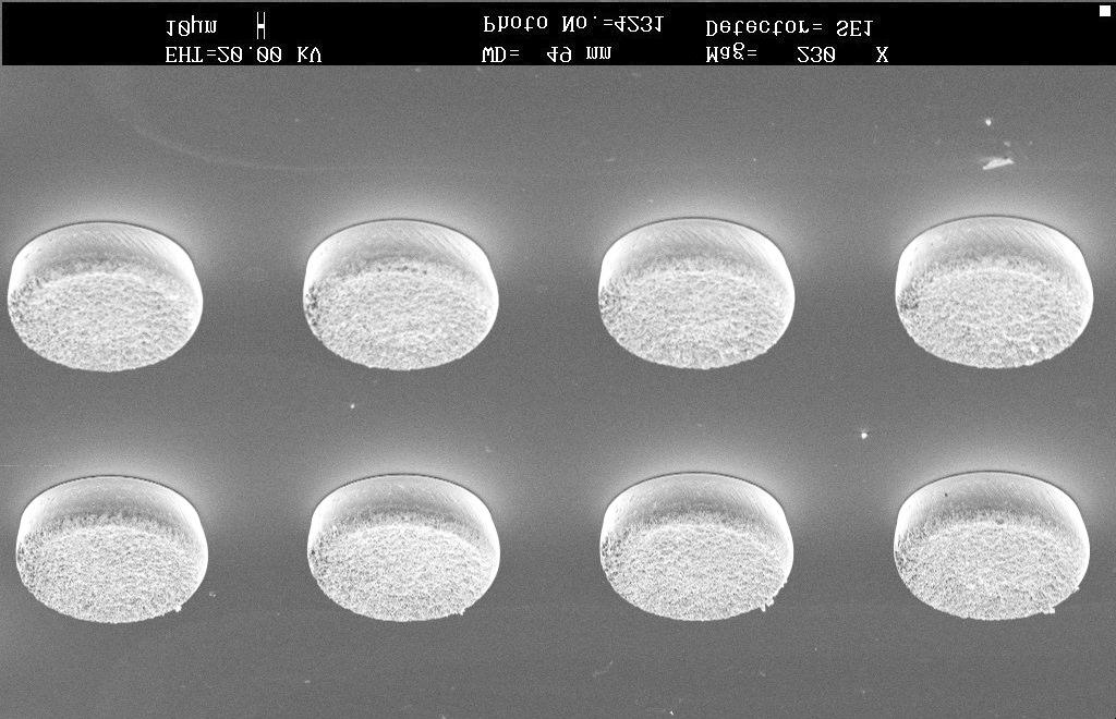
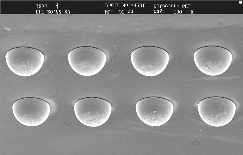
5 Fig. 3a. SEM of as-plated pure-tin bumps Fig. 3b. SEM of re-flowed pure-tin bumps Fig. 4a. SEM of as-plated tin-bismuth solder bumps Fig. 4b. SEM of re-flowed tin-bismuth solder bumps Fig. 5a. SEM of as-plated tin-copper solder bumps Fig. 5b. SEM of re-flowed tin-copper solder bumps


6 Fig. 6a. SEM of as-plated tin-silver solder bumps Fig. 6b. SEM of re-flowed tin-silver solder bumps Fig. 7a. SEM of as-plated tin-silver-copper solder bumps (fabricated by sequential plating of tin-silver and tincopper) Fig. 7b. SEM of re-flowed tin-silver-copper solder bumps Fig. 8a. SEM of re-flowed cross-sectioned tin-silver bump at the interface between the copper UBM and solder bump Fig. 8b. SAM of re-flowed cross-sectioned tin-silver bump showing the distribution of copper at the interface between the copper UBM and solder bump


 showing the interface between the copper UBM, nickel")
 showing the distribution of copper at the interface")
7 Fig. 8c. SAM of re-flowed cross-sectioned tin-silver bump showing the distribution of tin at the interface between the copper UBM and solder bump Fig. 8d. SAM of re-flowed cross-sectioned tin-silver bump showing the distribution of silver at the interface between the copper UBM and solder bump Fig. 9a. SEM of cross-sectioned eutectic lead-tin solder bump (after re-flow) showing the interface between the copper UBM, nickel cap, and solder bump Fig. 9b. SAM of cross-sectioned eutectic lead-tin solder bump (after re-flow) showing the distribution of copper at the interface between the copper UBM, nickel cap, and solder bump Fig. 9c. SAM of cross-sectioned eutectic lead-tin solder bump (after re-flow) showing the distribution of nickel at the interface between the copper UBM, nickel cap, and solder bump Fig. 9d. SAM of cross-sectioned eutectic lead-tin solder bump (after re-flow) showing the distribution of tin at the interface between the copper UBM, nickel cap, and solder bump
TIN-BASED LEAD-FREE SOLDER BUMPS FOR FLIP-CHIP APPLICATION. S. Yaakup, H. S. Zakaria, M. A. Hashim and A. Isnin
 TIN-BASED LEAD-FREE SOLDER BUMPS FOR FLIP-CHIP APPLICATION S. Yaakup, H. S. Zakaria, M. A. Hashim and A. Isnin Advanced Materials Research Centre (AMREC), SIRIM Berhad, Lot 34, Jalan Hi-Tech 2/3, Kulim
Supplementary Materials for
 www.sciencemag.org/cgi/content/full/336/6084/1007/dc1 Supplementary Materials for Unidirectional Growth of Microbumps on (111)-Oriented and Nanotwinned Copper Hsiang-Yao Hsiao, Chien-Min Liu, Han-wen Lin,
Lead Free Solder for Flip Chip
 Lead Free Solder for Flip Chip Zhenwei Hou & R. Wayne Johnson Laboratory for Electronics Assembly & Packaging Auburn University 162 Broun Hall, ECE Dept. Auburn, AL 36489 USA 334-844-1880 johnson@eng.auburn.edu
Atmosphere Effect on Soldering of Flip Chip Assemblies. C. C. Dong Air Products and Chemicals, Inc. U.S.A.
 Atmosphere Effect on Soldering of Flip Chip Assemblies C. C. Dong Air Products and Chemicals, Inc. U.S.A. Atmosphere Effect on Soldering of Flip Chip Assemblies Abstract An experimental study was conducted
Developments in low-temperature metal-based packaging
 Developments in low-temperature metal-based packaging 2011. 12.14 Jiyoung Chang and Liwei Lin Ph.D. Candidate, Department of Mechanical Engineering University of California at Berkeley 1 1 Contents Project
Effect of Process Variations on Solder Joint Reliability for Nickel-based Surface Finishes
 Effect of Process Variations on Solder Joint Reliability for Nickel-based Surface Finishes Hugh Roberts Atotech USA Inc., Rock Hill, SC, USA Sven Lamprecht, Gustavo Ramos and Christian Sebald Atotech Deutschland
Ultra Fine Pitch Bumping Using e-ni/au and Sn Lift-Off Processes
 Ultra Fine Pitch Bumping Using e-ni/au and Sn Lift-Off Processes Andrew Strandjord, Thorsten Teutsch, and Jing Li Pac Tech USA Packaging Technologies, Inc. Santa Clara, CA USA 95050 Thomas Oppert, and
THE EFFECTS OF INTERNAL STRESSRS IN BGA Ni LAYER ON THE STRENGTH OF Sn/Ag/Cu SOLDER JOINT
 THE EFFECTS OF INTERNAL STRESSRS IN BGA Ni LAYER ON THE STRENGTH OF Sn/Ag/Cu SOLDER JOINT C.H. Chien 1, * C.J. Tseng 1,2 T.P. Chen 1,3 1 Department of Mechanical and Electro-Mechanical Engineering, National
RELIABILITY IMPACT OF COPPER-DOPED EUTECTIC TIN-LEAD BUMP AND ITS VOIDING UPON FLIP CHIP ASSEMBLIES
 RELIABILITY IMPACT OF COPPER-DOPED EUTECTIC TIN-LEAD BUMP AND ITS VOIDING UPON FLIP CHIP ASSEMBLIES David Ihms and Shing Yeh Delphi Electronics & Safety Kokomo, IN, USA david.w.ihms@delphi.com and shing.yeh@delphi.com
Flip Chip Bump Electromigration Reliability: A comparison of Cu Pillar, High Pb, SnAg, and SnPb Bump Structures
 Flip Chip Bump Electromigration Reliability: A comparison of Cu Pillar,,, and SnPb Bump Structures Ahmer Syed, Karthikeyan Dhandapani, Lou Nicholls, Robert Moody, CJ Berry, and Robert Darveaux Amkor Technology
3D-WLCSP Package Technology: Processing and Reliability Characterization
 3D-WLCSP Package Technology: Processing and Reliability Characterization, Paul N. Houston, Brian Lewis, Fei Xie, Ph.D., Zhaozhi Li, Ph.D.* ENGENT Inc. * Auburn University ENGENT, Inc. 2012 1 Outline Packaging
JOINT INDUSTRY STANDARD
 JOINT INDUSTRY STANDARD AUGUST 1999 Semiconductor Design Standard for Flip Chip Applications ASSOCIATION CONNECTING ELECTRONICS INDUSTRIES Semiconductor Design Standard for Flip Chip Applications About
Adaption to scientific and technical progress under Directive 2002/95/EC
 . Adaption to scientific and technical progress under Directive 2002/95/EC Results previous evaluation Exemption No. 15 Lead in solders to complete a viable electrical connection between semiconductor
Maximum MAX662 12V DC-DC Converter
 Construction Analysis Maximum MAX662 12V DC-DC Converter Report Number: SCA 9512-445 Global Semiconductor Industry the Serving Since 1964 17350 N. Hartford Drive Scottsdale, AZ 85255 Phone: 602-515-9780
Adaption to scientific and technical progress under Directive 2002/95/EC
 . Adaption to scientific and technical progress under Directive 2002/95/EC Results previous evaluation Exemption No. 7 a a) Lead in high melting temperature type solders (i.e. lead-based alloys containing
Reliability of Lead-Free Solder Connections for Area-Array Packages
 Presented at IPC SMEMA Council APEX SM 2001 For additional information, please email marketing@amkor.com Reliability of Lead-Free Solder Connections for Area-Array Packages Ahmer Syed Amkor Technology,
Future Electronic Devices Technology in Cosmic Space and Electroless Ni/Pd/Au Plating for High Density Semiconductor Package Substrate
 JAXA 25 rd Microelectronics Workshop Future Electronic Devices Technology in Cosmic Space and Electroless Ni/Pd/Au Plating for High Density Semiconductor Package Substrate November 2, 2012 Yoshinori Ejiri
A study aimed at characterizing the interfacial structure in a tin silver solder on nickel-coated copper plate during aging
 Sādhanā Vol. 33, Part 3, June 2008, pp. 251 259. Printed in India A study aimed at characterizing the interfacial structure in a tin silver solder on nickel-coated copper plate during aging D C LIN 1,
Electrical and Fluidic Microbumps and Interconnects for 3D-IC and Silicon Interposer
 Electrical and Fluidic Microbumps and Interconnects for 3D-IC and Silicon Interposer Li Zheng, Student Member, IEEE, and Muhannad S. Bakir, Senior Member, IEEE Georgia Institute of Technology Atlanta,
Study of the Interface Microstructure of Sn-Ag-Cu Lead-Free Solders and the Effect of Solder Volume on Intermetallic Layer Formation.
 Study of the Interface Microstructure of Sn-Ag-Cu Lead-Free Solders and the Effect of Solder Volume on Intermetallic Layer Formation. B. Salam +, N. N. Ekere, D. Rajkumar Electronics Manufacturing Engineering
Motorola MC68360EM25VC Communication Controller
 Construction Analysis EM25VC Communication Controller Report Number: SCA 9711-562 Global Semiconductor Industry the Serving Since 1964 17350 N. Hartford Drive Scottsdale, AZ 85255 Phone: 602-515-9780 Fax:
Advanced Analytical Techniques for Semiconductor Assembly Materials and Processes. Jason Chou and Sze Pei Lim Indium Corporation
 Advanced Analytical Techniques for Semiconductor Assembly Materials and Processes Jason Chou and Sze Pei Lim Indium Corporation Agenda Company introduction Semiconductor assembly roadmap challenges Fine
Ultralow Residue Semiconductor Grade Fluxes for Copper Pillar Flip-Chip
 Ultralow Residue Semiconductor Grade Fluxes for Copper Pillar Flip-Chip SzePei Lim (Presenter), Jason Chou, Maria Durham, and Dr. Andy Mackie Indium Corporation 1 Outline of Presentation Roadmaps and challenges
High-Temperature-Resistant Interconnections Formed by Using Nickel Micro-plating and Ni Nano-particles for Power Devices
 Kato et al.: High-Temperature-Resistant Interconnections (1/6) [Technical Paper] High-Temperature-Resistant Interconnections Formed by Using Nickel Micro-plating and Ni Nano-particles for Power Devices
Lead-Free Connectors - An Overview
 Lead-Free Connectors - An Overview Pete Elmgren Molex Inc. 15 August 2003 Introduction For more than 50 years, lead-bearing solders have been used almost exclusively throughout the electronics industry
EN287. Switching to lead-free solder raises many issues and has consequences for all parts of the printed circuit board (PCB) assembly process.
 assembly process.") EN287 Switching to lead-free solder raises many issues and has consequences for all parts of the printed circuit board (PCB) assembly process. This leaflet explains why companies need to consider making
EN287 Switching to lead-free solder raises many issues and has consequences for all parts of the printed circuit board (PCB) assembly process. This leaflet explains why companies need to consider making
By Ron Blankenhorn, Pac Tech USA, Santa Clara, Calif., and Thomas Oppert, Pac Tech GbmH, Nauen, Germany
 INTRODUCTION Modern microelectronic products require packages that address the driving forces of reduced size and weight, as well as increased performance at high frequencies. Flipchip and direct chip
FYS4260/FYS9260: Microsystems and Electronics Packaging and Interconnect. Metallization and Interconnects
 FYS4260/FYS9260: Microsystems and Electronics Packaging and Interconnect Metallization and Interconnects Learning objectives Metal heros Significance of selecting right metallization systems and examples
Ball shear strength and fracture mode of lead-free solder joints prepared using nickel nanoparticle doped flux
 Ball shear strength and fracture mode of lead-free solder joints prepared using nickel nanoparticle doped flux G. K. Sujan a, A. S. M. A. Haseeb a, *, Chong Hoe Jian b, Amalina Afifi a a Department of
Interfacial Reactions between the Sn-9Zn Solder and Au/Ni/SUS304 Multi-layer Substrate
 , July 6-8, 2011, London, U.K. Interfacial Reactions between the Sn-9Zn Solder and Au/Ni/SUS304 Multi-layer Substrate *Yee-Wen Yen 1, Chien-Chung Jao 2, Kuo-Sing Chao 1, Shu-Mei Fu Abstract Sn-9Zn lead-free
Fraunhofer IZM Bump Bonding and Electronic Packaging
 Fraunhofer IZM Bump Bonding and Electronic Packaging Fraunhofer Institute for Reliability and Microintegration (IZM) Gustav-Meyer-Allee 25 13355 Berlin Germany Dipl.-Ing. Thomas Fritzsch Contact: thomas.fritzsch@izm.fraunhofer.de
The Morphology Evolution and Voiding of Solder Joints on QFN Central Pads with a Ni/Au Finish
 The Morphology Evolution and Voiding of Solder Joints on QFN Central Pads with a Ni/Au Finish Julie Silk 1, Jianbiao Pan 2, Mike Powers 1 1 Agilent Technologies, 1400 Fountaingrove Parkway, Santa Rosa,
Characterization of Coined Solder Bumps on PCB Pads
 Characterization of Coined Solder Bumps on PCB Pads Jae-Woong Nah, Kyung W. Paik, Won-Hoe Kim*, and Ki-Rok Hur** Department of Materials Sci. & Eng., Korea Advanced Institute of Science and Technology
Composition/wt% Bal SA2 (SABI) Bal SA3 (SABI + Cu) Bal
 Bal SA3 (SABI + Cu) Bal") Improving Thermal Cycle and Mechanical Drop Impact Resistance of a Lead-free Tin-Silver-Bismuth-Indium Solder Alloy with Minor Doping of Copper Additive Takehiro Wada 1, Seiji Tsuchiya 1, Shantanu Joshi
Improving Thermal Cycle and Mechanical Drop Impact Resistance of a Lead-free Tin-Silver-Bismuth-Indium Solder Alloy with Minor Doping of Copper Additive Takehiro Wada 1, Seiji Tsuchiya 1, Shantanu Joshi
Dallas Semicoductor DS80C320 Microcontroller
 Construction Analysis Dallas Semicoductor DS80C320 Microcontroller Report Number: SCA 9702-525 Global Semiconductor Industry the Serving Since 1964 15022 N. 75th Street Scottsdale, AZ 85260-2476 Phone:
PROCESSING AND RELIABILITY OF LOW-SILVER-ALLOYS
 PROCESSING AND RELIABILITY OF LOW-SILVER-ALLOYS Mathias Nowottnick and Andrej Novikov University of Rostock Rostock, Germany mathias.nowottnick@uni-rostock.de Joerg Trodler W.C. Heraeus Hanau, Germany
Reflow Profiling: Time a bove Liquidus
 Reflow Profiling: Time a bove Liquidus AIM/David Suraski Despite much research and discussion on the subject of reflow profiling, many questions and a good deal of confusion still exist. What is clear
NPL REPORT MAT 6. Preliminary Measurements for Thermoplastic Electronics: Developing a Stress Screening Test. M WICKHAM, L ZOU and C HUNT
 NPL REPORT MAT 6 Preliminary Measurements for Thermoplastic Electronics: Developing a Stress Screening Test M WICKHAM, L ZOU and C HUNT NOT RESTRICTED NOVEMBER 7 Preliminary Measurements for Thermoplastic
Undercooling, Microstructures and Hardness of Sn-Rich Pb-Free Solders on Cu-xZn Alloy Under Bump Metallurgies
 Materials Transactions, Vol. 50, No. 9 (2009) pp. 2291 to 2296 #2009 The Japan Institute of Metals Undercooling, Microstructures and Hardness of Sn-Rich Pb-Free Solders -xzn Alloy Under Bump Metallurgies
Design for Flip-Chip and Chip-Size Package Technology
 Design for Flip-Chip and Chip-Size Package Technology Vern Solberg Solberg Technology Consulting Madison, Wisconsin Abstract As new generations of electronic products emerge they often surpass the capability
The Effect of Fillers in Nonconductive Adhesive on the Reliability of Chip-on-Glass Bonding with Sn/Cu Bumps
 Materials Transactions, Vol. 52, No. 11 (2011) pp. 2106 to 2110 #2011 The Japan Institute of Metals The Effect of Fillers in Nonconductive Adhesive on the Reliability of Chip-on-Glass Bonding with Sn/Cu
Optimizing Immersion Silver Chemistries For Copper
 Optimizing Immersion Silver Chemistries For Copper Ms Dagmara Charyk, Mr. Tom Tyson, Mr. Eric Stafstrom, Dr. Ron Morrissey, Technic Inc Cranston RI Abstract: Immersion silver chemistry has been promoted
Manufacturing of electronic equipment
 Manufacturing of electronic equipment 13.10.2016 Objective: To give a generic understanding on the manufacturing methods and 2 nd level interconnection materials of electronic equipments Literature: K.
Evaluation of Cu Pillar Chemistries
 Presented at 2016 IMAPS Device Packaging Evaluation of Cu Pillar Chemistries imaps Device Packaging Conference Spring 2016 Matthew Thorseth, Mark Scalisi, Inho Lee, Sang-Min Park, Yil-Hak Lee, Jonathan
Effect of Reflow Profile (RSP Vs RTP) on Sn/Ag/Cu Solder Joint Strength in Electronic Packaging
 on Sn/Ag/Cu Solder Joint Strength in Electronic Packaging") ISSN 2231-8798 2012 UniKLBMI Effect of Reflow Profile (RSP Vs RTP) on Sn/Ag/Cu Solder Joint Strength in Electronic Packaging I. Ahmad 1, A. Jalar 2 Z. Kornain 3 & U. Hashim 4 1 Universiti Tenaga Nasional
ISSN 2231-8798 2012 UniKLBMI Effect of Reflow Profile (RSP Vs RTP) on Sn/Ag/Cu Solder Joint Strength in Electronic Packaging I. Ahmad 1, A. Jalar 2 Z. Kornain 3 & U. Hashim 4 1 Universiti Tenaga Nasional
Tin Whisker Prevention with SnBi Plating
 Tin Whisker Prevention with SnBi Plating Issei Fujimura, Manager of R&D Section No. 2, Ishihara Chemical Co., Ltd. 5-26 Nishiyanagiwara-cho, Hyogo-ku, Kobe, Hyogo 652-0806, Japan E. Jan Vardaman and Dr.
Basic PCB Level Assembly Process Methodology for 3D Package-on-Package
 Basic PCB Level Assembly Process Methodology for 3D Package-on-Package Vern Solberg STC-Madison Madison, Wisconsin USA Abstract The motivation for developing higher density IC packaging continues to be
Freescale Semiconductor Tape Ball Grid Array (TBGA) Overview
 Overview") Freescale Semiconductor Tape Ball Grid Array (TBGA) Overview Revision 0 2006 Freescale and the Freescale logo are trademarks of Freescale Semiconductor, Inc. All other product or service names are the
Freescale Semiconductor Tape Ball Grid Array (TBGA) Overview Revision 0 2006 Freescale and the Freescale logo are trademarks of Freescale Semiconductor, Inc. All other product or service names are the
THE EFFECTS OF PLATING MATERIALS, BOND PAD SIZE AND BOND PAD GEOMETRY ON SOLDER BALL SHEAR STRENGTH
 THE EFFECTS OF PLATING MATERIALS, BOND PAD SIZE AND BOND PAD GEOMETRY ON SOLDER BALL SHEAR STRENGTH Keith Rogers and Craig Hillman CALCE Electronic Products and Systems Center University of Maryland College
Self-Organized Interconnection Process Using Solderable ACA (Anisotropic Conductive Adhesive)
") Materials Transactions, Vol. 50, No. 7 (2009) pp. 1684 to 1689 Special Issue on New Functions and Properties of Engineering Materials Created by Designing and Processing #2009 The Japan Institute of Metals
Materials Transactions, Vol. 50, No. 7 (2009) pp. 1684 to 1689 Special Issue on New Functions and Properties of Engineering Materials Created by Designing and Processing #2009 The Japan Institute of Metals
Interconnect Structure for Room Temperature 3D-IC Stacking Employing Binary Alloying for High Temperature Stability
 Minapad 2014, May 21 22th, Grenoble; France Interconnect Structure for Room Temperature 3D-IC Stacking Employing Binary Alloying for High Temperature Stability Eric Schulte 1, Keith Cooper 1 Matthew Lueck
Effect of Multiple Flip-Chip Assembly on Joint Strength of AuSn solder in Hybrid Compact Optoelectronic Module
 1 Effect of Multiple Flip-Chip Assembly on Joint Strength of AuSn solder in Hybrid Compact Optoelectronic Module K.-M. Chu, Student Member, IEEE, J.-S. Lee, H. Oppermann, G. Engelmann, J. Wolf, H. Reichl,
Future Electronic Devices Technology in Cosmic Space and Lead-free Solder Joint Reliability
 The 22nd Microelectronics Work Future Electronic Devices Technology in Cosmic Space and Lead-free Solder Joint Reliability Key Points (1) High Speed Solder Ball Shear Test (2) Relationship between Surface
Sn623-5T-E SOLDER PASTE
 Sn623-5T-E SOLDER PASTE INTRODUCTION Singapore Asahi s solder paste Sn623-5T-E is a silver bearing paste to prevent silver migration and brittleness. It is formulated for fine pitch applications up to
Shear Strength in Solder Bump Joints for High Reliability Photodiode Packages
 Materials Transactions, Vol. 44, No. 10 (2003) pp. 2163 to 2168 #2003 The Japan Institute of Metals Shear Strength in Solder Bump Joints for High Reliability Photodiode Packages Chong-Hee Yu 1, Kyung-Seob
DITF ToolKit 1. Standard Substrate Sizes (selected at the factory for optimum process)
") DITF ToolKit 1 DITF Toolkit Substrates Common Substrate Materials Alumina (99.5% min) єr = 9.9 Tan d = 1.5 x10⁻⁴ Aluminum Nitride (K170) єr = 8.9 Tan d = 2.0 x10⁻³ Beryllia (99.5%) єr = 6.7 Tan d = 3.0
DITF ToolKit 1 DITF Toolkit Substrates Common Substrate Materials Alumina (99.5% min) єr = 9.9 Tan d = 1.5 x10⁻⁴ Aluminum Nitride (K170) єr = 8.9 Tan d = 2.0 x10⁻³ Beryllia (99.5%) єr = 6.7 Tan d = 3.0
Interfacial Reactions of Ni-doped SAC105 and SAC405 Solders on Ni-Au Finish during Multiple Reflows
 Interfacial Reactions of Ni-doped SAC105 and Solders on Ni-Au Finish during Multiple Reflows Toh C.H. 1, Liu Hao 1, Tu C.T 2., Chen T.D. 2, and Jessica Yeo 1 1 United Test and Assembly Center Ltd, 5 Serangoon
WF6317. A superactive low-volatile/high heat-resistant water-soluble flux for ball soldering
 WF637 A superactive low-volatile/high heat-resistant water-soluble flux for ball soldering Low viscosity and high tacking power stabilize ball holding force and ensures excellent solder wettability Easy
MARCH National Physical Laboratory Hampton Road Teddington Middlesex United Kingdom TW11 0LW
 NPL REPORT DEPC-MPR 044 Measuring the Impact of Land Size and Solder Joint Volume on Lead-free Solder Joint Reliability M Wickham, L Zou, M Dusek and C P Hunt NOT RESTRICTED MARCH 2006 National Physical
Growth Kinetics of Reaction Layers in Flip Chip Joints with Cu-cored Lead-free Solder Balls
 Materials Transactions, Vol. 5, No. 3 () pp. 75 to 75 Special Issue on Lead-Free Soldering in Electronics # The Japan Institute of Metals Growth Kinetics of Reaction Layers in Flip Chip Joints with Cu-cored
Welcome to the Real World of Lead Free Soldering
 Welcome to the Real World of Lead Free Soldering Metallic Resources, Inc. Howard Stevens Nimal Liyanage,, Ph.D Objective: to Provide Education Regarding the Effects of Various Lead Free Soldering Alloys
Impacts of the bulk Phosphorous content of electroless Nickel layers to Solder Joint Integrity
 Impacts of the bulk Phosphorous content of electroless Nickel layers to Solder Joint Integrity Sven Lamprecht, Kuldip Johal, Dr. H.-J. Schreier, Hugh Roberts Atotech Deutschland GmbH Atotech USA, Berlin
Reliability And Processability Of Sn/Ag/Cu Solder Bumped Flip Chip Components On Organic High Density Substrates
 Reliability And Processability Of Sn/Ag/Cu Solder Bumped Flip Chip Components On Organic High Density Substrates Minja Penttilä, Kauppi Kujala Nokia Mobile Phones, Research and Technology Access Itamerenkatu
Micron Semiconductor MT5C64K16A1DJ 64K x 16 SRAM
 Construction Analysis Micron Semiconductor MT5C64K16A1DJ 64K x 16 SRAM Report Number: SCA 9412-394 Global Semiconductor Industry the Serving Since 1964 17350 N. Hartford Drive Scottsdale, AZ 85255 Phone:
Interfacial reactions of BGA Sn 3.5%Ag 0.5%Cu and Sn 3.5%Ag solders during high-temperature aging with Ni/Au metallization
 Materials Science and Engineering B 113 (2004) 184 189 Interfacial reactions of BGA Sn 3.5%Ag 0.5%Cu and Sn 3.5%Ag solders during high-temperature aging with Ni/Au metallization Ahmed Sharif, M.N. Islam,
UMC UM F-7 2M-Bit SRAM
 Construction Analysis UMC UM 613264F-7 2M-Bit SRAM Report Number: SCA 9609-511 Global Semiconductor Industry the Serving Since 1964 15022 N. 75th Street Scottsdale, AZ 85260-2476 Phone: 602-998-9780 Fax:
Optimizing Immersion Silver Chemistries For Copper
 Optimizing Immersion Silver Chemistries For Copper Ms Dagmara Charyk, Mr. Tom Tyson, Mr. Eric Stafstrom, Dr. Ron Morrissey, Technic Inc Cranston RI Abstract: Immersion silver chemistry has been promoted
HYPRES. Hypres MCM Process Design Rules 04/12/2016
 HYPRES Hypres MCM Process Design Rules 04/12/2016 Direct all inquiries, questions, comments and suggestions concerning these design rules and/or HYPRES fabrication to: Daniel T. Yohannes Tel. (914) 592-1190
Evaluation of Pb-free BGA Solder Joint Reliability on Ni-based Surface Finishes using Alternative Shear and Pull Metrologies
 Evaluation of Pb-free BGA Solder Joint Reliability on Ni-based Surface Finishes using Alternative Shear and Pull Metrologies Kuldip Johal and Hugh Roberts Atotech USA Inc., Rock Hill, SC Sven Lamprecht,
BOARD LEVEL RELIABILITY COMPARISON OF LEAD FREE ALLOYS
 BOARD LEVEL RELIABILITY COMPARISON OF LEAD FREE ALLOYS Robert Darveaux, Corey Reichman, Sabira Enayet, Wen-Sung Hsu, and Win Thandar Swe Amkor Technology, Inc. Chandler, AZ, USA rdarv@amkor.com ABSTRACT
Jacques Matteau. NanoBond Assembly: A Rapid, Room Temperature Soldering Process. Global Sales Manager. indium.us/f018
 Jacques Matteau Global Sales Manager NanoBond Assembly: A Rapid, Room Temperature Soldering Process jmatteau@indium.com indium.us/f014 indium.us/f018 Terminology A few key terms NanoFoil is the heat source
Technology Drivers for Plasma Prior to Wire Bonding
 Technology Drivers for Plasma Prior to Wire Bonding James D. Getty Nordson MARCH Concord, CA, USA info@nordsonmarch.com Technology Drivers for Plasma Prior to Wire Bonding Page 1 ABSTRACT Advanced packaging
Copyright 2008 Year IEEE. Reprinted from IEEE ECTC May 2008, Florida USA.. This material is posted here with permission of the IEEE.
 Copyright 8 Year IEEE. Reprinted from IEEE ECTC 8. 7 - May 8, Florida USA.. This material is posted here with permission of the IEEE. Such permission of the IEEE does not in any way imply IEEE endorsement
1 Thin-film applications to microelectronic technology
 1 Thin-film applications to microelectronic technology 1.1 Introduction Layered thin-film structures are used in microelectronic, opto-electronic, flat panel display, and electronic packaging technologies.
Reaction of Sn-Bearing Solders with Nickel-based Under Bump Metallisations
 STR/03/069/ST Reaction of Sn-Bearing Solders with Nickel-based Under Bump Metallisations G. Qi, M. He and Z. Chen Abstract This work relates to wafer bumping technologies for flip chip packaging applications
How Bad's the Damage?
 How Bad's the Damage? Evaluating Probe Damage On Aluminum, Solder, Gold, UBM, and Copper Pads. Ken Smith Vice President of Technology Development Pyramid Probe Division, Cascade Microtech Goal of Presentation
Motorola MPA1016FN FPGA
 Construction Analysis Motorola MPA1016FN FPGA Report Number: SCA 9711-561 Global Semiconductor Industry the Serving Since 1964 17350 N. Hartford Drive Scottsdale, AZ 85255 Phone: 602-515-9780 Fax: 602-515-9781
Palladium as diffusion barrier - a way to a multifunctional printed circuit board finish
 Palladium as diffusion barrier - a way to a multifunctional printed circuit board finish Dr. Norbert Sitte, Schwaebisch Gmuend, Umicore Galvanotechnik GmbH 1. Introduction Due to the continuing miniaturization
Bridging Supply Chain Gap for Exempt High-Reliability OEM s
 Bridging Supply Chain Gap for Exempt High-Reliability OEM s Hal Rotchadl hrotchadl@premiers2.com www.premiers2.com Premier Semiconductor Services Tempe, AZ RoHS exempt high reliability OEMs breathed a
Development of gold to gold interconnection flip chip bonding for chip on suspension assemblies
 Microelectronics Reliability 42 (2002) 381 389 www.elsevier.com/locate/microrel Development of gold to gold interconnection flip chip bonding for chip on suspension assemblies C.F. Luk a,1, Y.C. Chan b,
Electroless Nickel / Electroless Palladium / Immersion Gold Process For Multi-Purpose Assembly Technology
 ckel / Palladium / Gold Process For Multi-Purpose Assembly Technology Kuldip Johal and Hugh Roberts, Atotech USA Inc. Sven Lamprecht, Atotech Deutschland GmbH ABSTRACT As the second part to a paper presented
General Introduction to Microstructure Technology p. 1 What is Microstructure Technology? p. 1 From Microstructure Technology to Microsystems
 General Introduction to Microstructure Technology p. 1 What is Microstructure Technology? p. 1 From Microstructure Technology to Microsystems Technology p. 9 The Parallels to Microelectronics p. 15 The
Rockwell R RF to IF Down Converter
 Construction Analysis Rockwell R6732-13 RF to IF Down Converter Report Number: SCA 9709-552 Global Semiconductor Industry the Serving Since 1964 17350 N. Hartford Drive Scottsdale, AZ 85255 Phone: 602-515-9780
Pulse White Paper Regarding RoHS Compliance
 Pulse White Paper Regarding RoHS Compliance Table of Contents Executive Summary... 2 Background/History... 3 Materials Selection... 3 Testing/Validation... 4 Implementation/Conclusion... 5 References...
Development of a Fluxless Flip Chip Bonding Process for Optical Military Electronics
 Development of a Fluxless Flip Chip Bonding Process for Optical Military Electronics Michael Girardi, Daric Laughlin, Philip Abel, Steve Goldammer, John Smoot NNSA s Kansas City Plant managed by Honeywell
Component Palladium Lead Finish - Specification Approved by Executive Board 1997-xx-xx August 22 Version
 Component Palladium Lead Finish - Specification Approved by Executive Board 1997-xx-xx August 22 Version Appendices 1. User Commitment Form 2. Supplier Compliance Form Table of contents 1. Background 2.
Investigation of the recommended immersion Tin thickness for Pbfree
 Investigation of the recommended immersion Tin thickness for Pbfree soldering Sven Lamprecht Atotech Deutschland GmbH Berlin Abstract First choices for Pb-free soldering are SnAgCu alloys, which are in
MECHANICAL PROPERTIES OF Sn3.5Ag AND Sn3.8Ag0.7Cu SOLDER BALLS FOR BGA PACKAGE
 221 MECHANICAL PROPERTIES OF AND Sn3.8Ag0.7Cu SOLDER BALLS FOR BGA PACKAGE A. Jalar 1, B.Y. Majlis 2, I.Ahmad 2 and E.P. Leng 3 1 School of Applied Physics, University Kebangsaan Malaysia, Selangor, Malaysia
EFFECT OF THERMAL AGING ON THE IMC LAYER BETWEEN SnAgSb SOLDER AND Cu SUBSTRATE. Universiti Kebangsaan Malaysia, 43600, Bangi, Selangor, Malaysia
 EFFECT OF THERMAL AGING ON THE IMC LAYER BETWEEN SnAgSb SOLDER AND Cu SUBSTRATE W. Shualdi 1, I. Ahmad 1, G. Omar 2 and A. Isnin 3 1 Department of Electrical, Electronic and System, Faculty of Engineering,
1.3.2 Nanotechnology Nanoporosity Deposition Methods Dissolution Methods
 Table of Contents 1. Metal Finishing 1 1.1 Introduction 1 1.1.1 Description of Industrial Activity Covered 1 1.1.2 Environmental and Legislative Background 3 1.1.3 Emerging Technology or Research? 4 1.2
VOIDS IN SOLDER JOINTS. Raiyo Aspandiar Intel Corporation
 VOIDS IN SOLDER JOINTS Raiyo Aspandiar Intel Corporation raiyo.f.aspandiar@intel.com Presented at SMTA Boise Expo and Tech Forum, March 20, 2018 Contents Introduction to Solder Voids Various Types of Voids
Development and characterization of novel metallic joint in power electronic device
 Development and characterization of novel metallic joint in power electronic device Guillaume LACOMBE 1-a, Jean-Marc HEINTZ 1-b, Akira KAWASAKI 2-c, Jean-François SILVAIN 1-d 1 CNRS, Université de Bordeaux,
MEPTEC Semiconductor Packaging Technology Symposium
 MEPTEC Semiconductor Packaging Technology Symposium Advanced Packaging s Interconnect Technology Process Shift and Direction October 23, 2014 Jay Hayes- Director of Business Development -Bumping and Flip
Comparative Study of NiNiP Leadframes from Different Processes
 Comparative Study of NiNiP Leadframes from Different Processes Wu-Hu Li *1, Jeffrey Khai Huat Low 1, Harry Sax 2, Raymond Solis Cabral 1, Esperidion De Castro Salazar 1, Pauline Min Wee Low 1 1 Infineon
2.5D and 3D Semiconductor Package Technology: Evolution and Innovation
 2.5D and 3D Semiconductor Package Technology: Evolution and Innovation Vern Solberg Solberg Technical Consulting Saratoga, California USA Abstract The electronics industry is experiencing a renaissance
ENHANCING WLCSP RELIABILITY THROUGH BUILD-UP STRUCTURE IMPROVEMENTS AND NEW SOLDER ALLOYS
 ENHANCING WLCSP RELIABILITY THROUGH BUILD-UP STRUCTURE IMPROVEMENTS AND NEW SOLDER ALLOYS B. Rogers, M. Melgo, M. Almonte, S. Jayaraman, C. Scanlan, and T. Olson Deca Technologies, Inc 7855 S. River Parkway,
Lead Free Surface Mount Technology. Ian Wilding BSc Senior Applications Engineer Henkel Technologies
 Lead Free Surface Mount Technology Ian Wilding BSc Senior Applications Engineer Henkel Technologies Overview of the Presentation First contact: Impact on the production operator Packaging Labelling Impact
Australian Journal of Basic and Applied Sciences. Pb-Free Solder Ball Robustness Comparison under AC and TC Reliability Test
 AENSI Journals Australian Journal of Basic and Applied Sciences ISSN:1991-8178 Journal home page: www.ajbasweb.com Pb-Free Solder Ball Robustness Comparison under AC and TC Reliability Test 1,2 Tan Cai
SN100C Technical Guide
 SN100C Technical Guide INTRODUCTION SN100C is a lead-free tin/copper//germanium alloy. It has been in use since about the year 2000. Since then SN100C has become a world leading alloy in wave and selective