Silicon Wafers: Basic unit Silicon Wafers Basic processing unit 100, 150, 200, 300, 450 mm disk, mm thick Current industrial standard 300 mm
|
|
|
- Harry Crawford
- 6 years ago
- Views:
Transcription

 Typical")
 Wafer cost $10 - $100's 200 mm wafer weight")

1 Silicon Wafers: Basic unit Silicon Wafers Basic processing unit 100, 150, 200, 300, 450 mm disk, mm thick Current industrial standard 300 mm (12 inches) Most research labs 100, 150 mm wafers (ours 100) Typical process wafers/run Each wafer: 's of microchips (die) Wafer cost $10 - $100's 200 mm wafer weight Kg Typical processing costs $1200/wafer (200 mm) Typical processed wafer value $11,000 (all products, modest yield) Value/Mass of processed wafer $275,000/Kg

2 Production of Silicon Wafers Silicon starts as beach sand quartzite Most silicon used now is solar cell industry lower grade China dominates polycrystalline & solar grade 4.6 Megatonnes Japan makes 46% of chip grade silicon wafers

 boils at 31.")
3 Conversion of Raw Sand into Metallurgical Grade Silicon Step 1: Metallurgical Grade Silicon (MSG): 98% pure Start with white beach sand (quartzite or SiO 2 ) Use electric arc to melt in mixture of coal coke, wood at 2000 o C Carbon removes impurities: molten Si drawn from bottom SiO 2 + 2C Si + 2CO Takes considerable power: KWh/Kg of Si Step 2: Metallurgical Grade Silicon Chemical Purification Convert MSG powder to trichlorosilane (SiHCl 3 ) by reacting with anhydrous hydrogen chloride at 300 o C Chlorine reacts with impurities to give material like AlCl 3, Trichlorosilane (SiHCl 3 ) boils at 31.8 o C Submerged electrode arc furnace for metallic silicon production Metallurgical grade silicon (poly crystalline)
 or 10 13 /cm 3 Reduced by 10 8 from original values Step 4: Silicon Chemical Vapour Deposition")
 Called the Siemens process Total production 3 million")
4 Metallurgical Grade Silicon into Polycrystalline Silicon Step 3: Distill Trichlorosilane Impurities reduce to parts per billion atoms (ppba) or /cm 3 Reduced by 10 8 from original values Step 4: Silicon Chemical Vapour Deposition Gaseous trichlorosilane (SiHCl 3 ) reacted with Hydrogen SiHCl3 + 2H 2 2Si + 6 HCl Si deposits out on rods with large crystals: Polycyrstalline Result Electronic Grade Silicon (EGS) Called the Siemens process Total production 3 million Kg 1985
5 Czochralski Crystal Growth methods Czochralski (CZ) basic Silicon crystal growth method Melt Poly Si EGS at 1430 o C in quartz crucible Rotate crucible Bring counter rotating seed crystal to melt Slowly draw seed from melt Atoms of melt freeze out aligned with crystal planes of seed


6 Czochralski Crystal Growth As seed drawn from melt initially grow narrow neck Dislocations (incorrect crystal alignment stopped at neck) As slow rate of pull (withdrawal) crystal diameter grows to max Maintain constant rotate/pull rate for uniformity eg 20 cm/hr


7 Finished Czochralski Crystals Crystals up to 200, 300 and 400 mm now possible Limit is weight that can be held by seed end (tang) Bottom called the butt end Most recent advance: Magnetic Convection suppression Magnetic field induces force to prevent moving Si conductor
 Segregation ratio fraction of liquid dopant in solid N k = N Thus as crystal pulled melt dopant concentration changes with X, fraction of melt solidified (ie X=0 at the seed")
8 Movement of Impurities from Melt to Crystal To put dopants in wafer place impurity in melt Equilibrium concentration (solubility) different in solid, N s than in liquid N l (note solubilities often symbolized as C s, C l ) Segregation ratio fraction of liquid dopant in solid N k = N Thus as crystal pulled melt dopant concentration changes with X, fraction of melt solidified (ie X=0 at the seed end) N s = kn l0 s l ( ) [ k 1 X 1] Thus dopant concentration changes along length of crystal Thus impurities & dopants differ in each wafer Hence measure each wafer resistivity


9 Float Zone Crystallization Float Zone (FZ) produces smaller wafers Start with polycrystalline Si rod Touch rod to seed crystal Heat with moving Radio Frequency (RF) coil Melts road near coil Move melt front from crystal to end and back Leaves single crystal rod behind
10 Comparison of CZ and FZ wafers FZ better impurity, but smaller size Reason: FZ process move impurities to ends of rod
 200 mm (8 inch) common fabrication")
 Bastard size (only a few facilities) 100")
 Obsolete size: still used in research (special order:")
 Basically need to rebuild entire fab to")
11 Current Common Si Wafer Sizes 300 mm (12 inch) now in most state of art fabs (2001) 200 mm (8 inch) common fabrication (started 1995) 150 mm (6 inch) most 2nd level to front line fabs 125 mm (5 inch) Bastard size (only a few facilities) 100 mm (4 inch) Smallest production wafers: research 75 mm (3 inch) Obsolete size: still used in research (special order: more expensive than 4 inch) 450 mm (18 inch) experimental production (2017) Basically need to rebuild entire fab to change wafer size


12 Rod (Bole) Sawing Use diamond saws to cut Crystal rods Very thin blades Resulting slices called wafers Typical wafer about mm thick ( mm wafers) Lose nearly half material in cutting Large gain poly Si square wafers used for solar cells solar poly Si wafer
13 Wafers Polishing Wafers mechanically abrasive polished to reduce roughness Then chemical/mechanical polished Film thickness are 0.1 microns or smaller for devices Thus wafers polished to < 10 nm defects
14 Wafer Flatness Very important for holding wafers down Also for focusing of photolithography 100 mm: thickness mm, flats: primary mm, secondary mm
 Wafer costs: $10-$4 for 100 mm, $20 for 150 mm 300, 450 (and some 200) mm wafers use a notch for orientation Notch is 1 mm")
15 Flats and Wafer types Flats are cut in the single crystal rods Allows wafers can to orientated and identified Primary flat largest: used to orientate wafer Secondary (minor) flat position varies with crystal and conductivity type Also specify wafer by resistivity (ohm-cm) Wafer costs: $10-$4 for 100 mm, $20 for 150 mm 300, 450 (and some 200) mm wafers use a notch for orientation Notch is 1 mm deep at <110> orientation for <100> wafers
16 Thermal Oxidation and Growth of Insulators (Jaeger 3, Campbell 4) Key advantage of Si: Oxidation of Si into SiO 2 (glass) Major factor in making Silicon the main semiconductor Grown at high temperature in pure O 2 (dry) or steam (wet) Glass is chemically inert Glass makes hard, dielectric layer Note: density changes with oxide type: dry is denser than wet Dry thermal oxide 2.27 g/cc Wet thermal oxide 2.18 g/cc
17 Glass Use in Semiconductors Looking at MosFet shows some of Glass applications
18 Uses of Oxide Films in IC s Both furnace grown oxides and Chemical Deposited (CVD) CVD is where chemical reactions create the oxide Furnace oxide is denser greater hardness, chemical resistance Also better electrical characteristics Higher resistivity, dielectric constant and breakdown voltage

 Si + 2H 2O SiO2 + 2H 2 Furnace growth charts depend on wet/dry and")
19 Growth of Oxide Films Done at high temperature in oxidizing gas Thickness control and density determine process Dry oxidation (denser oxides: gate oxide) Si + O 2 SiO 2 Wet Oxidation (lower density: Thick masking, Field oxides) Si + 2H 2O SiO2 + 2H 2 Furnace growth charts depend on wet/dry and crystal orientation


20 Wet Oxidation Si <100> Furnace Growth Chart

21 Dry Oxidation Si <100> Furnace Growth Chart


22 Dry Oxidation Si <111> Furnace Growth Chart
23 Furnace Growth of Oxide Films Oxide grows both above original Si surface and into the Si surface Si layer thickness decreased by 0.44 x o Wafer gains weight from oxide Weight change depends difference in density of Si from SiO 2 Note: Dry oxide has higher density than wet oxide
24 Good Oxide Growth Processes Start with removing wafers from storage Clean wafers (cleaning processes depends on previous processing) Load wafers into boat in Laminar Flow Hood (reduces particle contamination) Boat pushed slowly into furnace After time/temperature/gas cycle wafers removed Most important factor: Prevention of wafer contamination
 Old handling: wafer tweezers could damage")

25 Handling Wafers Wafers kept in a cassette (up to 25 wafers) Old handling: wafer tweezers could damage wafers, carry dirt Modern: Vacuum tweezers, pencils or wands clean, less damage but more likely to drop
26 Standard RCA Cleaning Process Standard clean of wafers before any hot process Not possible after any metal level depositions Process different for initial pre-oxidation, and post oxidation Chemicals & RCA Clean Always use Deionized (DI) Water Use Electronic Grade Chemicals 27% NH 4 OH (Ammonium Hydroxide) 30% unstabilized H 2 O 2 (Hydrogen Peroxide) 49% HF (Hydrofluroic Acid) 30% HCl (Hydrochloric Acid) Step Procedure Temp.( o C) Time (S) Purpose 1 12 parts H 2 O 2 parts NH 4 OH 3 parts H 2 O 2 80±5 600 Organic/ Metal Removal 2 Deionized water quench RT >120 Rinse 3 10 parts H 2 O 1 part HF *(100 part H 2 O for post oxidation) RT 30 Si surface removal 4 Deionized water quench RT >120 Rinse 5 14 parts H 2 O 2 parts HCl 3 parts H 2 O 2 6 Deionized water cascade rinse (3 rinses) 7 Spin Dry 8 N 2 blow dry 80±5 600 Heavy Metal RT Removal 300 each Rinse
27 Cascade Rinse Rinse in DI water to remove contaminates DI water production limited, so must control use Cascade 3 level final rinse Place wafers in lower level (twice used water) Move to 2nd level (once used water) Top level final clean
28 Spin Dry Spin wafer to remove water Spin up wafer to 1000 rpm Removes water Some left on back of wafer Blow with high speed N 2 to remove
29 Wafers Loading Wafers loaded into quartz boats Loading done in Laminar Flow Hoods Wafer loading depends on style of boat Most common Craddle type (used here) Wafers perpendicular to gas flow get high density Slotted has wafers parallel to gas flow Flat/slab has wafers lying flat usually done for CVD process


30 Wafers in Boat in Oxidation Furnace Generally loading from back to front Start with some trailing buffer wafers -makes flow more uniform Then add process wafers must be straight in quartz boat Watch for wafers sticking in boat slots Note location of specific wafers in boat Wafer thickness and uniformity depends on position Add monitor wafers for future film measurements Usually have several monitor wafers some get other processes Have one monitor that only sees this process Add leading buffer wafers to make flow uniform at process area
31 Oxidation Furnace Furnace is at elevate temperature Wafers loaded slowly into furnace to prevent thermal shock Manual loading for oxide growth load at lower T than oxidation Production fabs use autoloaders that move wafers in very slowly Then can load furnace at oxidation temp Problem for research labs auto loader is as big as furnace

32 3 Zone Oxidation Furnace Furnace have 3 heat zones Each heat zone separately controlled heating coils Temperature of outer zones adjusted to keep central zone flat T.
33 Furnace Temperature Programs Furnaces under computer control Load wafers below 800 o C Ramp up temperature to oxidation level rate limited by power of furnace Temp. flat during oxidation Cool down ramp, limited by cool rate Problem takes long time to ramp up and down Hence production Fabs load more slowly at oxidation temp
34 Gas Flow in Oxidation Furnace Nitrogen atmosphere during ramp up and ramp down Little oxide growth them, keeps system clean During oxidation add Oxygen or steam Oxygen in Gas form Steam produced by Bubbler DI water in heater near 100 o C Oxygen bubbled through bubbler
35 Measuring Oxide thickness with Color Chart Rough measure of wafer by color appearance Optical interference in oxide selects colors Colors repeat in 1/2 wavelength of light in film Derived by Riezman and Van Gelder (1967) Accurate to ±2.5 nm Tyger measurement system in lab uses similar interference Works on non-absorbing films.

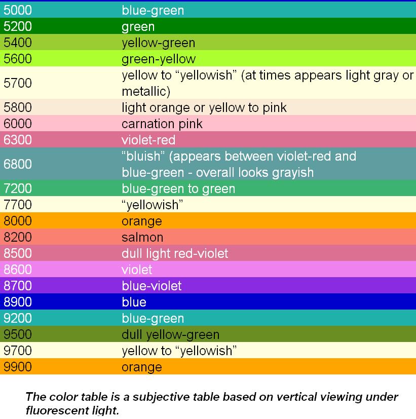
36 Oxide Thickness Colour Chart Good charts at and for > 1um thickness

37 Ellipsometry Film Measurement Non destructive optical measurement of transparent films Uses change of state of light polarization when reflected at angle from film Use lasers as light source Complicated calculations now done automatically Problem: Telling order of 1/2 wavelengths Need two measurements for that Index of refraction of oxide typically 1.45 Alternative: profile measurement of thickness after etching
38 Thermal Oxidation Theory Consider a Si wafer with a surface oxide of thickness x o in an oxidizing gas at some temperature T N G = Density of oxidant in the gas Three operations occur in oxidation: Oxidant flows in at gas/oxide interface with flux j 1 (x o ) Oxidant diffuses through oxide with flux j 2 (x) x = distance above Si surface Oxidant consumed by reaction at Si/oxide interface j 3 (x=0)
39 Thermal Oxidation Theory Flow at gas/sio 2 Surface: j 1 Flux is atoms/molecules passing given surface per unite time (unites atoms/cm 2 sec) Oxidant declines from gas level N G to SiO 2 surface due to flux into oxide Flux flow a mass transport process At oxide surface (x = x o ) the flux into the oxide is j [ N N( )] 1 = h G x0 where h = mass transfer coefficient or proportionality constant N(x o ) = oxidant concentration at SiO 2 surface h is related to diffusion of oxidant from gas to oxide and thickness of slow moving gas layer at surface Within oxide (0 << x << x o ): j 2 Oxidant flow decreases linearly from the surface level j 2 ( x) N = D ( x ) N( 0) where D = Diffusion coefficient of oxidant in SiO 2 N(0) = oxidant concentration at Si surface Related to Fick's diffusion law 0 x 0
40 Reaction of Oxide at Si Surface: j 3 Reaction Rate of oxide in Si surface j ( x ) k N( 0) 3 0 = where k s = reaction rate constant Relating Flux at Interfaces Oxidant is consumed only at Si: Thus under steady state s j = 1 = j2 j3 Thus solving for the oxidant concentration at 0 and x o N N ( 0) ( x ) 0 = 1 + NG ks + h ksx D 0 ksx0 NG 1 + D = ks ksx h D Growth of oxide thickness is related to reaction rate by dx dt 0 = k N γ ( 0) where γ = no. of oxidant molecules used per unit oxide volume γ = 2.2x10 22 cm -2 for O 2 (Dry oxidation) γ = 4.4x10 22 cm -2 for H 2 O (Wet oxidation) s 0
41 Thermal Oxidation Solutions: Grove's Law Combining this with N(0) formula dx γ dt 0 = 1 + ksn ks + h G ksx D Deal and Grove (1965) solved this assuming x o (t=0) = x i with 2 x0 0 + Ax = B t A = 2D B = τ = x 1 k s 0 ( +τ ) + 2DN G γ 2 i + Ax B 1 h Thus start with film x i which is defined to have taken time τ and grow for additional time t 2 then get film thickness of x ( t +τ ) 0 2 ie: Result same as growing the film continuously for time t = t 2 + τ Does not matter which oxidation process used for x i time used is calculated for the process of the new growth not for process used to actually grow oxide Then solve the quadratic equation for x 0, using A, B & τ Dry oxidation has an initial τ at t=0 while wet oxide does not i
42 Thermal Oxidation Regions Two main Regions Linear Rate Constant When start growth limited by reaction rate when ( t +τ ) x 0 B A 2 A << 4B ( t +τ ) Parabolic Rate Constant Reaction is limited by diffusion mass transport when ( t +τ ) x 2 0 B 2 A >> 4B ( t +τ )
43 Changes of Oxidation Rate Constants Reaction rate k s only depends on Si-Si bond Thus linear rate coefficient is B A ksh NG = ks + h γ k s NG γ h experimentally has small effect Parabolic rate coefficient follows an Arrhenius equation Assumes molecules must exceed an activation energy for reaction B = B 0 Ea exp kt where T = absolute temperature (K) E a = activation energy (ev) k = Boltzman's constant = 1.38x10⁻²³ J/K = 8.62x10⁻⁵ ev/k
44 Parabolic Rate Constants For Arrhenius plot Parabolic rate vs 1000/T Shows activation energy lower for wet oxidation (0.71 ev) than for dry (1.24 ev) Linear parameter plot E a = 1.92eV
45 Trapped Chargeq in Oxide Films Trapped charge in dielectric films very important Has large effect on device behaviour, especially MOSFET's Trapped charge creates part of Gate Threshold Voltage Reason why MOSFET technology very process sensitive Trapped charges from 4 main sources Interface Charge Q it Located directly at Si-SiO 2 interface Caused by structural Si defects from oxidation metallic impurities or bond breaking at interface Removed by low temp. anneal: 450 o C for 30 min Q it ~ charges/cm 2 Fixed Oxide Charge Q f Q f usually positive In oxide within 3.5 nm of Si-SiO 2 interface Caused by oxidation: depends on temperature & cooling rate Slow cooling: low fixed charge Not removable after formation (hence fixed charge) must compensate with dopants Q f ~ charges/cm 2
46 Trap Charge in Oxide film Con'd Mobile Ionic Charge Q m Q m from highly mobile ions of impurities Worse are sodium, potassium and lithium (positive charges) Ions move in oxide at room temp. Q m ~ charges/cm 2 Most dangerous to devices: must control impurities Oxide Trapped Charge Q ot Q ot either positive or negative Defects in oxide from radiation, static charges Q it ~ charges/cm 2
47 Measurement of Trapped Charges Measurement of trapped charge very important for Mosfets Done by making a metal/oxide/si capacitor Measure variation of capacitance with applied voltage Called C-V curves (see Campbell 4.5)
Thermal Oxidation and Growth of Insulators (Chapter 3 - Jaeger 3) Key advantage of Si: Oxidation of Si into SiO 2 (glass) Major factor in making
 Key advantage of Si: Oxidation of Si into SiO 2 (glass) Major factor in making") Thermal Oxidation and Growth of Insulators (Chapter 3 - Jaeger 3) Key advantage of Si: Oxidation of Si into SiO (glass) Major factor in making Silicon the main semiconductor Grown at high temperature in
Thermal Oxidation and Growth of Insulators (Chapter 3 - Jaeger 3) Key advantage of Si: Oxidation of Si into SiO (glass) Major factor in making Silicon the main semiconductor Grown at high temperature in
Chapter 2 Crystal Growth and Wafer Preparation
 Chapter 2 Crystal Growth and Wafer Preparation Professor Paul K. Chu Advantages of Si over Ge Si has a larger bandgap (1.1 ev for Si versus 0.66 ev for Ge) Si devices can operate at a higher temperature
Physics and Material Science of Semiconductor Nanostructures
 Physics and Material Science of Semiconductor Nanostructures PHYS 570P Prof. Oana Malis Email: omalis@purdue.edu Today Bulk semiconductor growth Single crystal techniques Nanostructure fabrication Epitaxial
Crystal Growth and Wafer Fabrication. K.Sivasankaran, Assistant Professor (Senior), VLSI Division, School of Electronics Engineering, VIT
, VLSI Division, School of Electronics Engineering, VIT") Crystal Growth and Wafer Fabrication K.Sivasankaran, Assistant Professor (Senior), VLSI Division, School of Electronics Engineering, VIT Crystal growth Obtaining sand Raw Polysilicon Czochralski Process
Crystal Growth and Wafer Fabrication K.Sivasankaran, Assistant Professor (Senior), VLSI Division, School of Electronics Engineering, VIT Crystal growth Obtaining sand Raw Polysilicon Czochralski Process
Microelettronica. Planar Technology for Silicon Integrated Circuits Fabrication. 26/02/2017 A. Neviani - Microelettronica
 Microelettronica Planar Technology for Silicon Integrated Circuits Fabrication 26/02/2017 A. Neviani - Microelettronica Introduction Simplified crosssection of an nmosfet and a pmosfet Simplified crosssection
Section 4: Thermal Oxidation. Jaeger Chapter 3. EE143 - Ali Javey
 Section 4: Thermal Oxidation Jaeger Chapter 3 Properties of O Thermal O is amorphous. Weight Density =.0 gm/cm 3 Molecular Density =.3E molecules/cm 3 O Crystalline O [Quartz] =.65 gm/cm 3 (1) Excellent
Section 4: Thermal Oxidation. Jaeger Chapter 3
 Section 4: Thermal Oxidation Jaeger Chapter 3 Properties of O Thermal O is amorphous. Weight Density =.0 gm/cm 3 Molecular Density =.3E molecules/cm 3 O Crystalline O [Quartz] =.65 gm/cm 3 (1) Excellent
The lowest quality of silicon is the so- called metallurgical silicon. The source material of making metallurgical silicon is quartzite.
 ET3034TUx - 4.2 - Manufacturing of crystalline silicon We have various types of silicon wafers such as monocrystalline silicon and polycrystalline silicon. In this block I will give an answer to the question:
PY2N20 Material Properties and Phase Diagrams
 PY2N20 Material Properties and Phase Diagrams Lecture 9 P. Stamenov, PhD School of Physics, TCD PY2N20-9 Semiconductor Wafer Production - Si Czochralski Growth Growth from melt Melt 99.999999% pure polycrystalline
CHAPTER 4: Oxidation. Chapter 4 1. Oxidation of silicon is an important process in VLSI. The typical roles of SiO 2 are:
 Chapter 4 1 CHAPTER 4: Oxidation Oxidation of silicon is an important process in VLSI. The typical roles of SiO 2 are: 1. mask against implant or diffusion of dopant into silicon 2. surface passivation
Oxide Growth. 1. Introduction
 Oxide Growth 1. Introduction Development of high-quality silicon dioxide (SiO2) has helped to establish the dominance of silicon in the production of commercial integrated circuits. Among all the various
EE CRYSTAL GROWTH, WAFER FABRICATION AND BASIC PROPERTIES OF Si WAFERS- Chapter 3. Crystal Structure z a
 1 EE 1 FALL 1999-00 CRYSTAL GROWTH, WAFER FABRICATION AND BASIC PROPERTIES OF Si WAFERS- Chapter 3 z a B Crystal Structure z a z a C y y y A x x Cubic BCC FCC x Crystals are characterized by a unit cell
HOMEWORK 4 and 5. March 15, Homework is due on Monday March 30, 2009 in Class. Answer the following questions from the Course Textbook:
 HOMEWORK 4 and 5 March 15, 2009 Homework is due on Monday March 30, 2009 in Class. Chapter 7 Answer the following questions from the Course Textbook: 7.2, 7.3, 7.4, 7.5, 7.6*, 7.7, 7.9*, 7.10*, 7.16, 7.17*,
More on oxidation. Oxidation systems Measuring oxide thickness Substrate orientation Thin oxides Oxide quality Si/SiO2 interface Hafnium oxide
 More on oxidation Oxidation systems Measuring oxide thickness Substrate orientation Thin oxides Oxide quality Si/SiO2 interface Hafnium oxide EE 432/532 oxide measurements, etc 1 Oxidation systems silicon
CRYSTAL GROWTH, WAFER FABRICATION AND BASIC PROPERTIES OF Si WAFERS- Chapter 3. Crystal Structure z a
 CRYSTAL GROWTH, WAFER FABRICATION AND BASIC PROPERTIES OF Si WAFERS- Chapter 3 Crystal Growth, Si Wafers- Chapter 3 z a C y B z a y Crystal Structure z a y Crystals are characterized by a unit cell which
Fabrication Technology
 Fabrication Technology By B.G.Balagangadhar Department of Electronics and Communication Ghousia College of Engineering, Ramanagaram 1 OUTLINE Introduction Why Silicon The purity of Silicon Czochralski
Fabrication Process. Crystal Growth Doping Deposition Patterning Lithography Oxidation Ion Implementation CONCORDIA VLSI DESIGN LAB
 Fabrication Process Crystal Growth Doping Deposition Patterning Lithography Oxidation Ion Implementation 1 Fabrication- CMOS Process Starting Material Preparation 1. Produce Metallurgical Grade Silicon
Doping and Oxidation
 Technische Universität Graz Institute of Solid State Physics Doping and Oxidation Franssila: Chapters 13,14, 15 Peter Hadley Technische Universität Graz Institute of Solid State Physics Doping Add donors
Why silicon? Silicon oxide
 Oxidation Layering. Oxidation layering produces a thin layer of silicon dioxide, or oxide, on the substrate by exposing the wafer to a mixture of highpurity oxygen or water at ca. 1000 C (1800 F). Why
Lecture 2 Silicon Properties and Growth
 Lecture 2 Silicon Properties and Growth Chapters 1 & 2 Wolf and Tauber 1/63 Lecture 2 Why Silicon? Crystal Structure. Defects. Sand to Electronic Grade Polysilicon. Polycrystalline to Single Crystal Silicon.
Czochralski Crystal Growth
 Czochralski Crystal Growth Crystal Pulling Crystal Ingots Shaping and Polishing 300 mm wafer 1 2 Advantage of larger diameter wafers Wafer area larger Chip area larger 3 4 Large-Diameter Wafer Handling
The Physical Structure (NMOS)
") The Physical Structure (NMOS) Al SiO2 Field Oxide Gate oxide S n+ Polysilicon Gate Al SiO2 SiO2 D n+ L channel P Substrate Field Oxide contact Metal (S) n+ (G) L W n+ (D) Poly 1 3D Perspective 2 3 Fabrication
The Physical Structure (NMOS) Al SiO2 Field Oxide Gate oxide S n+ Polysilicon Gate Al SiO2 SiO2 D n+ L channel P Substrate Field Oxide contact Metal (S) n+ (G) L W n+ (D) Poly 1 3D Perspective 2 3 Fabrication
Chemical Vapour Deposition: CVD Reference: Jaeger Chapter 6 & Ruska: Chapter 8 CVD - Chemical Vapour Deposition React chemicals to create a thin film
 Chemical Vapour Deposition: CVD Reference: Jaeger Chapter 6 & Ruska: Chapter 8 CVD - Chemical Vapour Deposition React chemicals to create a thin film layer at the surface Typically gas phase reactions
Kinetics of Silicon Oxidation in a Rapid Thermal Processor
 Kinetics of Silicon Oxidation in a Rapid Thermal Processor Asad M. Haider, Ph.D. Texas Instruments Dallas, Texas USA Presentation at the National Center of Physics International Spring Week 2010 Islamabad
MICROCHIP MANUFACTURING by S. Wolf
 MICROCHIP MANUFACTURING by S. Wolf Chapter 13: THERMAL- OXIDATION of SILICON 2004 by LATTICE PRESS Chapter 13: THERMAL-OXIDATION of SILICON n CHAPTER CONTENTS Applications of Thermal Silicon-Dioxide Physical
Etching Etching Definitions Isotropic Etching: same in all direction Anisotropic Etching: direction sensitive Selectivity: etch rate difference
 Etching Etching Definitions Isotropic Etching: same in all direction Anisotropic Etching: direction sensitive Selectivity: etch rate difference between 2 materials Need strong selectivity from masking
Wafer Cleaning and Oxide Growth Laboratory Dr. Lynn Fuller Webpage:
 ROCHESTER INSTITUTE OF TECHNOLOGY MICROELECTRONIC ENGINEERING Wafer Cleaning and Oxide Growth Laboratory Dr. Lynn Fuller Webpage: http://www.rit.edu/~lffeee 82 Lomb Memorial Drive Rochester, NY 14623-5604
Chapter 4. UEEP2613 Microelectronic Fabrication. Oxidation
 Chapter 4 UEEP2613 Microelectronic Fabrication Oxidation Prepared by Dr. Lim Soo King 24 Jun 2012 Chapter 4...113 Oxidation...113 4.0 Introduction... 113 4.1 Chemistry of Silicon Dioxide Formation... 115
Thin Films: Sputtering Systems (Jaeger Ch 6 & Ruska Ch 7,) Can deposit any material on any substrate (in principal) Start with pumping down to high
 Can deposit any material on any substrate (in principal) Start with pumping down to high") Thin Films: Sputtering Systems (Jaeger Ch 6 & Ruska Ch 7,) Can deposit any material on any substrate (in principal) Start with pumping down to high vacuum ~10-7 torr Removes residual gases eg oxygen from
Thin Films: Sputtering Systems (Jaeger Ch 6 & Ruska Ch 7,) Can deposit any material on any substrate (in principal) Start with pumping down to high vacuum ~10-7 torr Removes residual gases eg oxygen from
Processing of Semiconducting Materials Prof. Pallab Banerjee Department of Material Science Indian Institute of Technology, Kharagpur
 Processing of Semiconducting Materials Prof. Pallab Banerjee Department of Material Science Indian Institute of Technology, Kharagpur Lecture - 35 Oxidation I (Refer Slide Time: 00:24) Today s topic of
ELEC 7364 Lecture Notes Summer Si Oxidation. by STELLA W. PANG. from The University of Michigan, Ann Arbor, MI, USA
 ELEC 7364 Lecture Notes Summer 2008 Si Oxidation by STELLA W. PANG from The University of Michigan, Ann Arbor, MI, USA Visiting Professor at The University of Hong Kong The University of Michigan Visiting
Chapter 5 Thermal Processes
 Chapter 5 Thermal Processes 1 Topics Introduction Hardware Oxidation Diffusion Annealing Post-Implantation Alloying Reflow High Temp CVD Epi Poly Silicon Nitride RTP RTA RTP Future Trends 2 Definition
EE THERMAL OXIDATION - Chapter 6. Basic Concepts
 EE 22 FALL 999-00 THERMAL OXIDATION - Chapter 6 Basic Concepts SiO 2 and the Si/SiO 2 interface are the principal reasons for silicon s dominance in the IC industry. SiO 2 : Easily selectively etched using
Instructor: Dr. M. Razaghi. Silicon Oxidation
 SILICON OXIDATION Silicon Oxidation Many different kinds of thin films are used to fabricate discrete devices and integrated circuits. Including: Thermal oxides Dielectric layers Polycrystalline silicon
THERMAL OXIDATION - Chapter 6 Basic Concepts
 THERMAL OXIDATION - Chapter 6 Basic Concepts SiO 2 and the Si/SiO 2 interface are the principal reasons for silicon s dominance in the IC industry. Oxide Thickness µm 0. µm 0 nm nm Thermally Grown Oxides
4. Thermal Oxidation. a) Equipment Atmospheric Furnace
 Equipment Atmospheric Furnace") 4. Thermal Oxidation a) Equipment Atmospheric Furnace Oxidation requires precise control of: temperature, T ambient gas, G time spent at any given T & G, t Vito Logiudice 34 4. Thermal Oxidation b) Mechanism
4. Thermal Oxidation a) Equipment Atmospheric Furnace Oxidation requires precise control of: temperature, T ambient gas, G time spent at any given T & G, t Vito Logiudice 34 4. Thermal Oxidation b) Mechanism
Crystalline Silicon Solar Cells
 12 Crystalline Silicon Solar Cells As we already discussed in Chapter 6, most semiconductor materials have a crystalline lattice structure. As a starting point for our discussion on crystalline silicon
Semiconductor Technology
 Semiconductor Technology from A to Z Oxidation www.halbleiter.org Contents Contents List of Figures List of Tables II III 1 Oxidation 1 1.1 Overview..................................... 1 1.1.1 Application...............................
Mostafa Soliman, Ph.D. May 5 th 2014
 Mostafa Soliman, Ph.D. May 5 th 2014 Mostafa Soliman, Ph.D. 1 Basic MEMS Processes Front-End Processes Back-End Processes 2 Mostafa Soliman, Ph.D. Wafers Deposition Lithography Etch Chips 1- Si Substrate
Defects and crystal growth
 CRYSTL GROWTH CRYSTL GROWTH steps and questions 1. Reactants in molten form Si 2. Transport to S/L interface 3. dsorbtion: entropy decreases -TDS increases DH decreases (exo) 4. Critical nucleus size DS
Solar Photovoltaic Technologies
 Solar Photovoltaic Technologies Lecture-29 Prof. C.S. Solanki Energy Systems Engineering IIT Bombay Contents Brief summary of the previous lecture Production of Si MG-Si, EG-Si Siemens Process, FBR process
Report 1. B. Starting Wafer Specs Number: 10 Total, 6 Device and 4 Test wafers
 Aaron Pederson EE 432 Lab Dr. Meng Lu netid: abp250 Lab instructor: Yunfei Zhao Report 1 A. Overview The goal of this lab is to go through the semiconductor fabrication process from start to finish. This
Fabrication and Layout
 ECEN454 Digital Integrated Circuit Design Fabrication and Layout ECEN 454 3.1 A Glimpse at MOS Device Polysilicon Aluminum ECEN 475 4.2 1 Material Classification Insulators Glass, diamond, silicon oxide
Silicon Epitaxial CVD Want to create very sharp PN boundary grow one type layer on other in single crystal form High dopant layers on low dopant
 Silicon Epitaxial CVD Want to create very sharp PN boundary grow one type layer on other in single crystal form High dopant layers on low dopant substrate Creates latch up protection for CMOS Buried Epi
Microelectronic Device Instructional Laboratory. Table of Contents
 Introduction Process Overview Microelectronic Device Instructional Laboratory Introduction Description Flowchart MOSFET Development Process Description Process Steps Cleaning Solvent Cleaning Photo Lithography
Silicon Oxides: SiO 2
 Silicon Oxides: SiO 2 Uses: diffusion masks surface passivation gate insulator (MOSFET) isolation, insulation Formation: grown / native thermal: highest quality anodization deposited: C V D, evaporate,
Lab 1: Field Oxide. Overview. Starting Wafers
 Overview Lab 1: Field Oxide Brandon Baxter, Robert Buckley, Tara Mina, Quentin Vingerhoets Lab instructor: Liang Zhang Course Instructor: Dr. Gary Tuttle EE 432-532 January 23, 2017 In this lab we created
Thin Films: Sputtering Systems (Jaeger Ch 6 & Ruska Ch 7,) Sputtering: gas plasma transfers atoms from target to substrate Can deposit any material
 Sputtering: gas plasma transfers atoms from target to substrate Can deposit any material") Thin Films: Sputtering Systems (Jaeger Ch 6 & Ruska Ch 7,) Sputtering: gas plasma transfers atoms from target to substrate Can deposit any material on any substrate (in principal) Start with pumping down
Thin Films: Sputtering Systems (Jaeger Ch 6 & Ruska Ch 7,) Sputtering: gas plasma transfers atoms from target to substrate Can deposit any material on any substrate (in principal) Start with pumping down
CL 240: Materials Technology
 CL 240: Materials Technology Semiconductor materials Instructor: Vinay Prasad Materials and processing - descriptive, few mathematical equations Semiconductors (Si), dopants, metals, insulators 34% of
EE 5344 Introduction to MEMS. CHAPTER 3 Conventional Si Processing
 3. Conventional licon Processing Micromachining, Microfabrication. EE 5344 Introduction to MEMS CHAPTER 3 Conventional Processing Why silicon? Abundant, cheap, easy to process. licon planar Integrated
Mikrosensorer. Microfabrication 1
 Mikrosensorer Microfabrication 1 Literature Introductory MEMS Fabrication and Applications Thomas M. Adams and Richard A. Layton Available as ebook on http://www.lub.lu.se/en/search/lubsearch.html This
Lab #2 Wafer Cleaning (RCA cleaning)
") Lab #2 Wafer Cleaning (RCA cleaning) RCA Cleaning System Used: Wet Bench 1, Bay1, Nanofabrication Center Chemicals Used: H 2 O : NH 4 OH : H 2 O 2 (5 : 1 : 1) H 2 O : HF (10 : 1) H 2 O : HCl : H 2 O 2
Lab #2 Wafer Cleaning (RCA cleaning) RCA Cleaning System Used: Wet Bench 1, Bay1, Nanofabrication Center Chemicals Used: H 2 O : NH 4 OH : H 2 O 2 (5 : 1 : 1) H 2 O : HF (10 : 1) H 2 O : HCl : H 2 O 2
Microstructure of Electronic Materials. Amorphous materials. Single-Crystal Material. Professor N Cheung, U.C. Berkeley
 Microstructure of Electronic Materials Amorphous materials Single-Crystal Material 1 The Si Atom The Si Crystal diamond structure High-performance semiconductor devices require defect-free crystals 2 Crystallographic
Silicon for Wafer production
 Silicon for Wafer production Introduction Production of Silicon Silicon is used in the semiconductor industry as raw material for the production of integrated circuits and solar cells. Integrated circuits
EE 432/532 CyMOS process PWELL Lithography & Diffusion Feb 24, 2016
 EE 432/532 CyMOS process PWELL Lithography & Diffusion Feb 24, 2016 Friday Afternoon Group Brady Koht Sebastian Roe Peter Bonnie Joseph Wickner Lab Instructor Yunfei Zhao 1. Overview Now that a Field Oxide
Ajay Kumar Gautam [VLSI TECHNOLOGY] VLSI Technology for 3RD Year ECE/EEE Uttarakhand Technical University
![Ajay Kumar Gautam [VLSI TECHNOLOGY] VLSI Technology for 3RD Year ECE/EEE Uttarakhand Technical University](/thumbs/75/72824557.jpg "Ajay Kumar Gautam [VLSI TECHNOLOGY] VLSI Technology for 3RD Year ECE/EEE Uttarakhand Technical University") 2014 Ajay Kumar Gautam [VLSI TECHNOLOGY] VLSI Technology for 3RD Year ECE/EEE Uttarakhand Technical University Page1 Syllabus UNIT 1 Introduction to VLSI Technology: Classification of ICs, Scale of integration,
2014 Ajay Kumar Gautam [VLSI TECHNOLOGY] VLSI Technology for 3RD Year ECE/EEE Uttarakhand Technical University Page1 Syllabus UNIT 1 Introduction to VLSI Technology: Classification of ICs, Scale of integration,
Semiconductor device fabrication
 REVIEW Semiconductor device fabrication is the process used to create the integrated circuits (silicon chips) that are present in everyday electrical and electronic devices. It is a multiplestep sequence
VLSI Digital Systems Design
 VLSI Digital Systems Design CMOS Processing cmpe222_03process_ppt.ppt 1 Si Purification Chemical purification of Si Zone refined Induction furnace Si ingot melted in localized zone Molten zone moved from
SiC crystal growth from vapor
 SiC crystal growth from vapor Because SiC dissolves in Si and other metals can be grown from melt-solutions: Liquid phase epitaxy (LPE) Solubility of C in liquid Si is 0.029% at 1700oC high T process;
Metallization deposition and etching. Material mainly taken from Campbell, UCCS
 Metallization deposition and etching Material mainly taken from Campbell, UCCS Application Metallization is back-end processing Metals used are aluminum and copper Mainly involves deposition and etching,
PHYS 534 (Fall 2008) Process Integration OUTLINE. Examples of PROCESS FLOW SEQUENCES. >Surface-Micromachined Beam
 Process Integration OUTLINE. Examples of PROCESS FLOW SEQUENCES. >Surface-Micromachined Beam") PHYS 534 (Fall 2008) Process Integration Srikar Vengallatore, McGill University 1 OUTLINE Examples of PROCESS FLOW SEQUENCES >Semiconductor diode >Surface-Micromachined Beam Critical Issues in Process
PHYS 534 (Fall 2008) Process Integration Srikar Vengallatore, McGill University 1 OUTLINE Examples of PROCESS FLOW SEQUENCES >Semiconductor diode >Surface-Micromachined Beam Critical Issues in Process
Lecture 22: Integrated circuit fabrication
 Lecture 22: Integrated circuit fabrication Contents 1 Introduction 1 2 Layering 4 3 Patterning 7 4 Doping 8 4.1 Thermal diffusion......................... 10 4.2 Ion implantation.........................
Chapter 2 MOS Fabrication Technology
 Chapter 2 MOS Fabrication Technology Abstract This chapter is concerned with the fabrication of metal oxide semiconductor (MOS) technology. Various processes such as wafer fabrication, oxidation, mask
Ion Implantation Most modern devices doped using ion implanters Ionize gas sources (single +, 2+ or 3+ ionization) Accelerate dopant ions to very
 Accelerate dopant ions to very") Ion Implantation Most modern devices doped using ion implanters Ionize gas sources (single +, 2+ or 3+ ionization) Accelerate dopant ions to very high voltages (10-600 KeV) Use analyzer to selection charge/mass
Ion Implantation Most modern devices doped using ion implanters Ionize gas sources (single +, 2+ or 3+ ionization) Accelerate dopant ions to very high voltages (10-600 KeV) Use analyzer to selection charge/mass
University of Texas Arlington Department of Electrical Engineering. Nanotechnology Microelectromechanical Systems Ph.D. Diagnostic Examination
 University of Texas Arlington Department of Electrical Engineering Nanotechnology Microelectromechanical Systems Ph.D. Diagnostic Examination Fall 2012 November 17, 2012 Question # 1 2 3 To be filled by
EE 330 Lecture 8. IC Fabrication Technology Part II. - Masking - Photolithography - Deposition - Etching - Diffusion
 EE 330 Lecture 8 IC Fabrication Technology Part II?? - Masking - Photolithography - Deposition - Etching - Diffusion Review from Last Time Technology Files Provide Information About Process Process Flow
Temperature Scales. Questions. Temperature Conversions 7/21/2010. EE580 Solar Cells Todd J. Kaiser. Thermally Activated Processes
 7/1/010 EE80 Solar Cells Todd J. Kaiser Flow of Wafer in Fabrication Lecture 0 Microfabrication A combination of Applied Chemistry, Physics and ptics Thermal Processes Diffusion & xidation Photolithograpy
Fabrication Technology, Part I
 EEL5225: Principles of MEMS Transducers (Fall 2003) Fabrication Technology, Part I Agenda: Oxidation, layer deposition (last lecture) Lithography Pattern Transfer (etching) Impurity Doping Reading: Senturia,
Figure 2.3 (cont., p. 60) (e) Block diagram of Pentium 4 processor with 42 million transistors (2000). [Courtesy Intel Corporation.
 (e) Block diagram of Pentium 4 processor with 42 million transistors (2000). [Courtesy Intel Corporation.") Figure 2.1 (p. 58) Basic fabrication steps in the silicon planar process: (a) oxide formation, (b) selective oxide removal, (c) deposition of dopant atoms on wafer, (d) diffusion of dopant atoms into exposed
Figure 2.1 (p. 58) Basic fabrication steps in the silicon planar process: (a) oxide formation, (b) selective oxide removal, (c) deposition of dopant atoms on wafer, (d) diffusion of dopant atoms into exposed
IC/MEMS Fabrication - Outline. Fabrication
 IC/MEMS Fabrication - Outline Fabrication overview Materials Wafer fabrication The Cycle: Deposition Lithography Etching Fabrication IC Fabrication Deposition Spin Casting PVD physical vapor deposition
Chapter 2 Manufacturing Process
 Digital Integrated Circuits A Design Perspective Chapter 2 Manufacturing Process 1 CMOS Process 2 CMOS Process (n-well) Both NMOS and PMOS must be built in the same silicon material. PMOS in n-well NMOS
Silicon VLSI Technology. Fundamentals, Practice and Modeling
 Text Book: Silicon VLSI Technology Fundamentals, Practice and Modeling Authors: J. D. Plummer, M. D. Deal, and P. B. Griffin Crystal Growth, Wafer Fab and Properties High Quality Single Crystal Wafers
Amorphous Materials Exam II 180 min Exam
 MIT3_071F14_ExamISolutio Name: Amorphous Materials Exam II 180 min Exam Problem 1 (30 Points) Problem 2 (24 Points) Problem 3 (28 Points) Problem 4 (28 Points) Total (110 Points) 1 Problem 1 Please briefly
Silicon Manufacturing
 Silicon Manufacturing Group Members Young Soon Song Nghia Nguyen Kei Wong Eyad Fanous Hanna Kim Steven Hsu th Fundamental Processing Steps 1.Silicon Manufacturing a) Czochralski method. b) Wafer Manufacturing
PDS Products PRODUCT DATA SHEET. BN-975 Wafers. Low Defect Boron Diffusion Systems. Features/Benefits BORON NITRIDE
 Low Defect Boron Diffusion Systems The purpose of the hydrogen injection process is to increase die yield per wafer. This is accomplished because the effects associated with the hydrogen injection process.
Silicon Epitaxial CVD Want to create very sharp PN boundary grow one type layer on other in single crystal form High dopant layers on low dopant
 Silicon Epitaxial CVD Want to create very sharp PN boundary grow one type layer on other in single crystal form High dopant layers on low dopant substrate Creates latch up protection for CMOS Buried Epi
Document version 1.1 September 2012
 Tool Identifier Boron, Phosphorous diffusion furnaces Document version 1.1 September 2012 Documented by Karthick Murukesan SAMPLE PREQUIREMENT: Sample should be either RCA cleaned or Piranha cleaned before
ME 141B: The MEMS Class Introduction to MEMS and MEMS Design. Sumita Pennathur UCSB
 ME 141B: The MEMS Class Introduction to MEMS and MEMS Design Sumita Pennathur UCSB Outline today Introduction to thin films Oxidation Deal-grove model CVD Epitaxy Electrodeposition 10/6/10 2/45 Creating
EE 330 Lecture 9. IC Fabrication Technology Part 2
 EE 330 Lecture 9 IC Fabrication Technology Part 2 Quiz 8 A 2m silicon crystal is cut into wafers using a wire saw. If the wire diameter is 220um and the wafer thickness is 350um, how many wafers will this
Lecture 4. Oxidation (applies to Si and SiC only) Reading: Chapter 4
 Reading: Chapter 4") Lecture 4 Oxidation (applies to Si and SiC only) Reading: Chapter 4 Introduction discussion: Oxidation: Si (and SiC) Only The ability to grow a high quality thermal oxide has propelled Si into the forefront
Lecture 4 Oxidation (applies to Si and SiC only) Reading: Chapter 4 Introduction discussion: Oxidation: Si (and SiC) Only The ability to grow a high quality thermal oxide has propelled Si into the forefront
ECE 440 Lecture 27 : Equilibrium P-N Junctions I Class Outline:
 ECE 440 Lecture 27 : Equilibrium P-N Junctions I Class Outline: Fabrication of p-n junctions Contact Potential Things you should know when you leave Key Questions What are the necessary steps to fabricate
Chapter 3 Silicon Device Fabrication Technology
 Chapter 3 Silicon Device Fabrication Technology Over 10 15 transistors (or 100,000 for every person in the world) are manufactured every year. VLSI (Very Large Scale Integration) ULSI (Ultra Large Scale
KGC SCIENTIFIC Making of a Chip
 KGC SCIENTIFIC www.kgcscientific.com Making of a Chip FROM THE SAND TO THE PACKAGE, A DIAGRAM TO UNDERSTAND HOW CPU IS MADE? Sand CPU CHAIN ANALYSIS OF SEMICONDUCTOR Material for manufacturing process
ELEC 3908, Physical Electronics, Lecture 4. Basic Integrated Circuit Processing
 ELEC 3908, Physical Electronics, Lecture 4 Basic Integrated Circuit Processing Lecture Outline Details of the physical structure of devices will be very important in developing models for electrical behavior
CS/ECE 5710/6710. N-type Transistor. N-type from the top. Diffusion Mask. Polysilicon Mask. CMOS Processing
 CS/ECE 5710/6710 CMOS Processing Addison-Wesley N-type Transistor D G +Vgs + Vds S N-type from the top i electrons - Diffusion Mask Mask for just the diffused regions Top view shows patterns that make
A discussion of crystal growth, lithography, etching, doping, and device structures is presented in
 Chapter 5 PROCESSING OF DEVICES A discussion of crystal growth, lithography, etching, doping, and device structures is presented in the following overview gures. SEMICONDUCTOR DEVICE PROCESSING: AN OVERVIEW
Chapter 3 CMOS processing technology
 Chapter 3 CMOS processing technology (How to make a CMOS?) Si + impurity acceptors(p-type) donors (n-type) p-type + n-type => pn junction (I-V) 3.1.1 (Wafer) Wafer = A disk of silicon (0.25 mm - 1 mm thick),
162 Solar Energy. front contact (metal grid) serial connections (to the back contact of the next cell) p-type wafer back contact
 serial connections (to the back contact of the next cell) p-type wafer back contact") 162 Solar Energy serial connections (to the back contact of the next cell) front contact (metal grid) antireflective coating n + -type emitter p + -type layer p-type wafer back contact 200 μm Figure 12.8:
162 Solar Energy serial connections (to the back contact of the next cell) front contact (metal grid) antireflective coating n + -type emitter p + -type layer p-type wafer back contact 200 μm Figure 12.8:
Microelectronics. Integrated circuits. Introduction to the IC technology M.Rencz 11 September, Expected decrease in line width
 Microelectronics Introduction to the IC technology M.Rencz 11 September, 2002 9/16/02 1/37 Integrated circuits Development is controlled by the roadmaps. Self-fulfilling predictions for the tendencies
VLSI Technology. By: Ajay Kumar Gautam
 By: Ajay Kumar Gautam Introduction to VLSI Technology, Crystal Growth, Oxidation, Epitaxial Process, Diffusion Process, Ion Implantation, Lithography, Etching, Metallization, VLSI Process Integration,
Increased Yield Using PDS Products Grade BN-975 with Hydrogen Injection
 Increased Yield Using PDS Products Grade BN-975 with Hydrogen Injection Technical Bulletin The purpose of the hydrogen injection process is to increase die yield per wafer. This is accomplished because
CHAPTER - 4 CMOS PROCESSING TECHNOLOGY
 CHAPTER - 4 CMOS PROCESSING TECHNOLOGY Samir kamal Spring 2018 4.1 CHAPTER OBJECTIVES 1. Introduce the CMOS designer to the technology that is responsible for the semiconductor devices that might be designed
Module 1 and 2 Report
 Module 1 and 2 Report Interdisciplinary Microelectronics Processing Lab Group D Jaimie Stevens, Erich P. Meinig, Adam Longoria, Emily Makoutz, Ben Timmer Date: February 10, 2015 Abstract This report details
MATERIALS. Silicon Wafers... J 04 J 01. MATERIALS / Inorganics & thin films guide
 J MATERIALS SUBSTRATES Silicon Wafers... J 04 J J 01 MATERIALS SUBSTRATES NEYCO has a complete range of crystal substrates for a wide variety of applications, including Semiconductor, Biotechnology, Nanotechnology,
Cleanroom, Wafer Clean and Gettering
 Principles of Micro- and Nanofabrication for Electronic and Photonic Devices Cleanroom, Wafer Clean and Gettering Xing Sheng 盛兴 Department of Electronic Engineering Tsinghua University xingsheng@tsinghua.edu.cn
Lecture #18 Fabrication OUTLINE
 Transistors on a Chip Lecture #18 Fabrication OUTLINE IC Fabrication Technology Introduction the task at hand Doping Oxidation Thin-film deposition Lithography Etch Lithography trends Plasma processing
Anodic Bonding And The Crack Opening Method Experiment. Individual Study ECE 199 Spring Quarter Advisors: Dr. Richard D.
 Anodic Bonding And The Crack Opening Method Experiment Individual Study ECE 199 Spring Quarter 2000 Advisors: Dr. Richard D. Nelson Allen Kine Research Students: Cop Van Le #50637990 Jun Kue Lee #50899208
Plasma-Enhanced Chemical Vapor Deposition
 Plasma-Enhanced Chemical Vapor Deposition Steven Glenn July 8, 2009 Thin Films Lab 4 ABSTRACT The objective of this lab was to explore lab and the Applied Materials P5000 from a different point of view.
Making of a Chip Illustrations
 Making of a Chip Illustrations 22nm 3D/Trigate Transistors Version April 2015 1 The illustrations on the following foils are low resolution images that visually support the explanations of the individual
Physical Vapor Deposition (PVD) Zheng Yang
 Zheng Yang") Physical Vapor Deposition (PVD) Zheng Yang ERF 3017, email: yangzhen@uic.edu Page 1 Major Fabrication Steps in MOS Process Flow UV light Mask oxygen Silicon dioxide photoresist exposed photoresist oxide
Physical Vapor Deposition (PVD) Zheng Yang ERF 3017, email: yangzhen@uic.edu Page 1 Major Fabrication Steps in MOS Process Flow UV light Mask oxygen Silicon dioxide photoresist exposed photoresist oxide