Roll-to-roll Vacuum Processing of Organic Thin Film Transistors
|
|
|
- Kevin Logan
- 6 years ago
- Views:
Transcription


1 Roll-to-roll Vacuum Processing of Organic Thin Film Transistors Hazel Assender Department of Materials University of Oxford DALMATIAN TECHNOLOGY 1


2 Aim of the Research To demonstrate the ability to fabricate all-evaporated transistors in a R2R vacuum web process environment exploiting the technology that is used in the packaging industry. - Flexible, polymer substrate (web) - High speed (e.g. 1m/s web speed) - R2R process - Low cost materials Possible application: anticounterfeiting/product tracking tags for packaging. 2
 Circuit design tailored for the properties achievable with this manufacturing route 3) Materials (organic semiconductor and polymer gate insulator layer) developed for this manufacturing route 4)")
3 Issues to consider 1) Process parameters in R2R environment building and testing transistors. 2) Circuit design tailored for the properties achievable with this manufacturing route 3) Materials (organic semiconductor and polymer gate insulator layer) developed for this manufacturing route 4) Patterning processes 5) Robustness of final devices Source and Drain (Metal) e.g. 90nm pentacene L Org. Semiconductor Gate Substrate W Insulator e.g. 0.5µm acrylic e.g. 125µm thick PEN 3
4 Roll-to-roll devices Gate insulator layer: Flash evaporated monomers then cure Perhaps surface modification layer: Various options Molecular semiconductor: Evaporation Source and Drain (Metal) Gate: pattern metallization Possible interlayer L W Org. Semiconductor Gate Insulator (e.g. acrylic dielectric) Source and Drain: pattern metallization Polymer smoothing layer: Flash evaporated monomers then cure Substrate (e.g. PET) Build complete device structure on the substrate Possible surface modification Encapsulation layer/gas barrier 4


5 Materials: pattern metallization Anilox Roller and Oil Boiler Winding zone Evaporation zone mbar Unwind Cliché Plate PRINTING RESOLUTION MD: micron TD: micron Process Drum Rewind Magnification x 60 Magnification x 200 { Source/Drain Electrodes------} 5


 iii.")
6 Depositing the gate-insulator In-line process High speed Smooth Acrylic layer Heat Tank 250 C Vacuum i. Evaporate monomer (liquid) ii. Monomer condenses onto substrate (web) as a liquid (flat) iii. Polymerize (cure) in-situ to a solid 6
7 Patterning the organic layers Insulator: Development of solventless printing (e.g. flexoprint and inkjet) of liquid monomer prior to e-beam or UV cure Semiconductor: High speed organic vapour jet printing. We have demonstrated working devices made with OVJP. Doctor blade Printing plate Cure Carrier gas in Nozzle Anilox roller Substrate Ink bath Gas out Gas heating furnace Semiconductor furnace 7
8 Gate insulator deposition V D (V) V D (V) I D (na) First devices V G -10V -20V -24V -30V -40V -44V Increase e-beam cure current I D (na) E-beam cured V G 0V -10V -20V -30V -40V 0 0 Anneal (150ºC 1hr) I D (µa) -1-10V -2-20V -30V -40V -3-50V V D (V) Plasma cured, single pass Make R2R process I D (µa) I on /I off = 1.3x10 3 V th = 15V µ = 0.1cm 2 /Vs -10V -20V -30V -40V V D (V) E-beam cured + annealed 8
 0.1 0.01 PNP PS PVS PBM TPGDA PMMA 0.01 0.")
9 Modification of the insulator surface Spin coat a thin (20-40nm) polymer layer: Ester:carbon ratio 1µm Mobility (cm 2 /Vs) PNP PS PVS PBM TPGDA PMMA Polar part surface energy (mn/m) 9
![Materials developments DNTT, dinaphtho[2,3-b:2,3 -f]thieno[3,2-b]thiophene, has better environmental stability due to a reduced](/docs-images/78/78171937/images/10-2.jpg "tendency to oxidize. Synthetic route for DNTT: DNTT synthesised and processed via A, literature route and B, an evolved method.")
10 Materials developments DNTT, dinaphtho[2,3-b:2,3 -f]thieno[3,2-b]thiophene, has better environmental stability due to a reduced tendency to oxidize. Synthetic route for DNTT: DNTT synthesised and processed via A, literature route and B, an evolved method. 10
11 DNTT devices TPGDA / DNTT TPGDA / Pentacene TPGDA / PS / DNTT TPGDA / PS / Pentacene V T (V) µ (cm 2 V -1 s -1 ) I on /I off S (V/decade) ± ± Yields, tested over batches of 96 transistors Made with solution-cast PS dielectric: 66% Made with evaporated TPGDA/PS dielectric: 100% V g (V) E I d (A) 1E-6 1E I d 0.5 (A 0.5 ) DNTT µ=1 cm 2 /Vs Pentaceneµ=0.6 cm 2 /Vs 1E-10 1E
12 Modelling DNTT devices I D (ma) Log 10 (I D /A) V D (V) Vg=-0.5V -2.5V -4.0V -30.0V V G (V) Vg=0V -5V -10V -15V -20V -25V -30V Parameter Solutiondeposited PS insulator Evaporated acrylic insulator Evaporated acrylic insulator with PS buffer Ambient Air Air Vacuum W(µm) L(µm) C i (nf/cm 2 ) V T (V) V 0 (V) V ACC µ ACC (cm 2 /Vs) γ x10-7 λ M SAT A SAT I 0 (fa) σ 0 (S) 7x x x10-13 R S (kω) R D (kω)
13 -V Invertor Enhancement Load V OUT V IN Driver OTFT Experimental Response Transfer Plot 13
14 Logic Circuits NAND NOR Truth Table NAND V IN 1 V IN 2 V OUT Truth Table NOR V IN 1 V IN 2 V OUT
15 Ring Oscillator V DD (V) Frequency (khz) Sim Expt Amplitude(V) Sim Expt
16 I d (A) 1E-4 1E-6 1E-8 1E-10 Environmental testing Vac Dry air DNTT with acrylate/ps insulator Vacuum vs. dry air Small V T shift Apparently stable performance over weeks if stored in dry conditions V g (V) Dry vs. damp air Increase in I off Mobility and V T unaffected Effect of water recoverable e.g. by exposing sample to vacuum. I d (A) 1E-4 1E-6 1E-8 1E-10 Dry air RH 50% V g (V) Lamination and in-line encapsulation (e.g. TPGDA followed by SiO x ) tried good working devices. 16
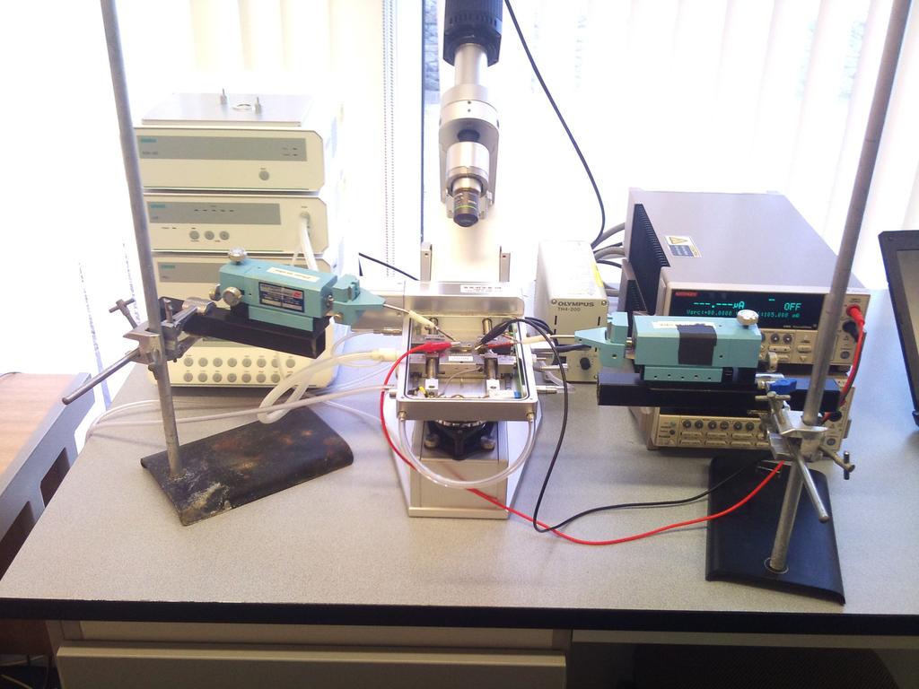
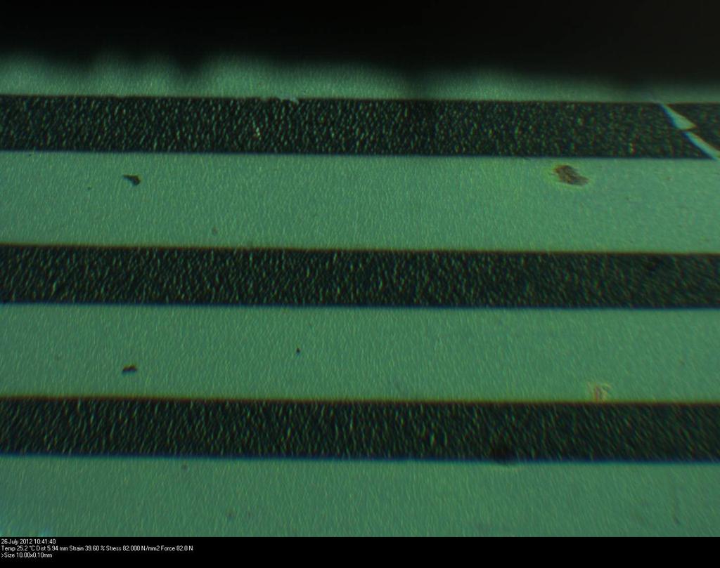
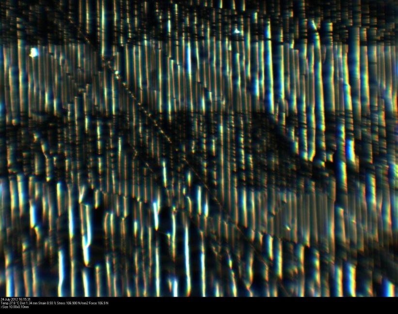

17 Mechanical testing Polymer dielectric 17th Oct 2013 AlOx dielectric 17
18 Progress so far.. 1) Process parameters in R2R environment building and testing transistors Plastic flexible substrates (125 µm thick PEN substrate) Al gate electrode Improved in-line curing method (10 m/min webspeed) Interface buffer layer (evaporated PS thin layer) Low hysteresis in devices and good stability Very high yield 18
19 Progress so far 2) Circuit design tailored for the properties achievable with this manufacturing route Transistor characteristics modelled 3) Materials (semiconductor and gate insulator layer) developed for this manufacturing route New SC synthesised, more under development Tried new insulator materials 4) Robustness of final devices Strain to failure much greater than devices with ceramic insulators Device mobility stable on bending Devices can survive lamination 5) Patterning processes Favoured options for SC and insulator layers under development 19
20 Acknowledgements Bangor Prof Martin Taylor Mr Aled Williams Mr Eifion Patchett Oxford Dr Gamal Abbas Mr Ziqian Ding Dr Kanad Mallik Leeds Prof Long Lin Dr Weidong He Manchester Prof Steve Yeates Dr John Morrison 20
EXCIMER LASER ANNEALING FOR LOW- TEMPERATURE POLYSILICON THIN FILM TRANSISTOR FABRICATION ON PLASTIC SUBSTRATES
 EXCIMER LASER ANNEALING FOR LOW- TEMPERATURE POLYSILICON THIN FILM TRANSISTOR FABRICATION ON PLASTIC SUBSTRATES G. Fortunato, A. Pecora, L. Maiolo, M. Cuscunà, D. Simeone, A. Minotti, and L. Mariucci CNR-IMM,
Applied Research for Vacuum Web Coating: What is Coming Next?
 Applied Research for Vacuum Web Coating: What is Coming Next? Matthias Fahland, John Fahlteich, Steffen Günther, Manuela Junghähnel, Claus Luber, Nicolas Schiller, Cindy Steiner, Steffen Straach, Michiel
From Vacuum to Atmosphere and back an in-house Process Chain for Different Products
 From Vacuum to Atmosphere and back an in-house Process Chain for Different Products Dr. Steffen Günther Vacuum coating low pressure 10-1 10-4 Pa (10-3 10-6 mbar) unhindered particle movement no unintended
The Effects of Defects on the Moisture-Barrier Performance of Clear Coatings on Polymer Substrates.
 AIMCAL, CHARLESTON, SC, 2013 The Effects of Defects on the Moisture-Barrier Performance of Clear Coatings on Polymer Substrates. The National Centre for Printed Electronics ALF part SMITH of Centre for
Flexible Electronics: Integration Processes for Organic and Inorganic Semiconductor-Based Thin-Film Transistors
 Electronics 2015, 4, 480-506; doi:10.3390/electronics4030480 Review OPEN ACCESS electronics ISSN 2079-9292 www.mdpi.com/journal/electronics Flexible Electronics: Integration Processes for Organic and Inorganic
Flexible functional devices at mass production level with the FLEx R2R sald platform
 Flexible functional devices at mass production level with the FLEx R2R sald platform D. Spee, W. Boonen, D. Borsa and E. Clerkx Meyer Burger (Netherlands) B.V. Meyer Burger Introduction to sald Challenges
Roll-to-roll Technology for Transparent High Barrier Films
 Roll-to-roll Technology for Transparent High Barrier Films Presented at the AIMCAL Fall Technical Conference, October 19-22, 2008, Myrtle Beach, SC, USA Nicolas Schiller, John Fahlteich, Matthias Fahland,
High-Resolution, Electrohydrodynamic Inkjet Printing of Stretchable, Metal Oxide Semiconductor Transistors with High Performances
 Electronic Supplementary Material (ESI) for Nanoscale. This journal is The Royal Society of Chemistry 2016 ` Electronic Supplementary Information High-Resolution, Electrohydrodynamic Inkjet Printing of
CONFERENCE EVALUATION FORM
 2015 AIMCAL Web Coating & Handling / SPE FlexPackCon CONFERENCE EVALUATION FORM To upgrade the quality of the Web Coating & Handling / FlexPackCon Conference, we would appreciate your comments. MONDAY,
Freshure Coatings: Environmentally Friendly Barrier Coatings
 Freshure Coatings: Environmentally Friendly Barrier Coatings Shahab Jahromi Knowfort Technologies BV Urmonderbaan 20a 6160MD Geleen The Netherlands Email: s.jahromi@knowfort.com Introduction. Roll-to-roll
"ITO Film Trend for Touch Panel Applications"
 AIMCAL Web Coating Conference 2011 October 23-26 Reno, Nevada USA 1 "ITO Film Trend for Touch Panel Applications" Teijin Chemicals Ltd. Haruhiko Itoh 2 Content 1. Structure and Features of TCF 2. Touch
Yung-Hui Yeh, and Bo-Cheng Kung Display Technology Center (DTC), Industrial Technology Research Institute, Hsinchu 310, Taiwan
, Industrial Technology Research Institute, Hsinchu 310, Taiwan") Amorphous In 2 O 3 -Ga 2 O 3 -ZnO Thin Film Transistors and Integrated Circuits on Flexible and Colorless Polyimide Substrates Hsing-Hung Hsieh, and Chung-Chih Wu* Graduate Institute of Electronics Engineering,
Amorphous In 2 O 3 -Ga 2 O 3 -ZnO Thin Film Transistors and Integrated Circuits on Flexible and Colorless Polyimide Substrates Hsing-Hung Hsieh, and Chung-Chih Wu* Graduate Institute of Electronics Engineering,
Aligned Carbon Nanofibre-Polymer Composite Membranes. CNT Growth and Manipulation. Eleanor Campbell Dept. of Physics, Göteborg University
 Aligned Carbon Nanofibre-Polymer Composite Membranes CNT Growth and Manipulation Eleanor Campbell Dept. of Physics, Göteborg University Plasma CVD Growth Polymer/Nanofibre Composite Low ambient temperature
Amorphous Oxide Transistor Electrokinetic Reflective Display on Flexible Glass
 Amorphous Oxide Transistor Electrokinetic Reflective Display on Flexible Glass Devin A. Mourey, Randy L. Hoffman, Sean M. Garner *, Arliena Holm, Brad Benson, Gregg Combs, James E. Abbott, Xinghua Li*,
EE40 Lec 22. IC Fabrication Technology. Prof. Nathan Cheung 11/19/2009
 Suggested Reading EE40 Lec 22 IC Fabrication Technology Prof. Nathan Cheung 11/19/2009 300mm Fab Tour http://www-03.ibm.com/technology/manufacturing/technology_tour_300mm_foundry.html Overview of IC Technology
IMRE/ETPL Flagship Project
 IMRE/ETPL Flagship Project Nanoparticulate Barrier Films & Gas Permeation Measurement Techniques for Thin Film Solar & Display Application Problems Senthil Ramadas Institute of Materials Research & Engineering
350 C for 8 hours in argon atmosphere. Supplementary Figures. Supplementary Figure 1 High-temperature annealing of BP flakes on SiO 2.
 Supplementary Figures Supplementary Figure 1 High-temperature annealing of BP flakes on SiO 2. (a-d) The optical images of three BP flakes on a SiO 2 substrate before (a,b) and after annealing (c,d) at
High Rate low pressure PECVD for barrier and optical coatings
 High Rate low pressure PECVD for barrier and optical coatings, Matthias Fahland, John Fahlteich, Björn Meyer, Steffen Straach, Nicolas Schiller Outline Introduction PECVD New developments magpecvd arcpecv
ABSTRACT: INTRODUCTION:
 ABSTRACT: Nano-Composite Polymer Optical Coatings Tom Faris Vampire Optical Coatings, Inc. P.O. Box 240 Kirkersville, Ohio 43033 (740)-927-5257 f(740)-927-5032 vampirecoatings@earthlink.net Traditionally
Lecture Day 2 Deposition
 Deposition Lecture Day 2 Deposition PVD - Physical Vapor Deposition E-beam Evaporation Thermal Evaporation (wire feed vs boat) Sputtering CVD - Chemical Vapor Deposition PECVD LPCVD MVD ALD MBE Plating
ITO SPUTTER COATED FILMS FOR TOUCH PANEL APPLICATIONS USING ROTARY SINTERED CERAMIC ITO TARGETS: WHAT CAN BE LEARNED FROM GLASS COATING?
 ITO SPUTTER COATED FILMS FOR TOUCH PANEL APPLICATIONS USING ROTARY SINTERED CERAMIC ITO TARGETS: WHAT CAN BE LEARNED FROM GLASS COATING? Paul Lippens AIMCAL Web coating conference 2012 Outline Introduction
Photonic Drying Pulsed Light as a low Temperature Sintering Process
 Photonic Drying Pulsed Light as a low Temperature Sintering Process Lou Panico Xenon Corporation W E S T E R N M I C H I G A N U N I V E R S I T Y PRESENTATION OVERVIEW What is Printed Electronics Materials
Large-area patterning by roller-based nanoimprint lithography
 JOANNEUM RESEARCH Forschungsgesellschaft Institute MATERIALS, Weiz, Austria Large-area patterning by roller-based nanoimprint lithography Ursula Palfinger, Dieter Nees, Stephan Ruttloff, Markus Leitgeb,
Nanotransfer Printing of Organic and Carbon Nanotube Thin-Film Transistors on Plastic Substrates
 Nanotransfer Printing of Organic and Carbon Nanotube Thin-Film Transistors on Plastic Substrates D. R. Hines, S. Mezhenny, M. Breban and E. D. Williams a) Laboratory for Physical Sciences and Department
An Improved Process for Fabricating High-Mobility Organic Molecular Crystal Field-Effect Transistors
 An Improved Process for Fabricating High-Mobility Organic Molecular Crystal Field-Effect Transistors A.P. Micolich a), L.L. Bell, and A.R. Hamilton School of Physics, University of New South Wales, Sydney
Barix Multilayers: a Water and Oxygen Barrier for Flexible Organic Electronics. Robert Jan Visser
 Barix Multilayers: a Water and Oxygen Barrier for Flexible Organic Electronics Robert Jan Visser Organic Electronics Is the Future of Electronics Organic? MIT Stanford UC Berkeley Nano Forum Vitex Systems,
LOW TEMPERATURE PHOTONIC SINTERING FOR PRINTED ELECTRONICS. Dr. Saad Ahmed XENON Corporation November 19, 2015
 LOW TEMPERATURE PHOTONIC SINTERING FOR PRINTED ELECTRONICS Dr. Saad Ahmed XENON Corporation November 19, 2015 Topics Introduction to Pulsed Light Photonic sintering for Printed Electronics R&D Tools for
Ultra High Barrier Coatings by PECVD
 Society of Vacuum Coaters 2014 Technical Conference Presentation Ultra High Barrier Coatings by PECVD John Madocks & Phong Ngo, General Plasma Inc., 546 E. 25 th Street, Tucson, Arizona, USA Abstract Silicon
Atomic Oxygen-Resistant, Static-Dissipative, Pinhole-Free Coatings for Spacecraft
 Physical Sciences Inc. VG10-109 Atomic Oxygen-Resistant, Static-Dissipative, Pinhole-Free Coatings for Spacecraft Michelle T. Schulberg, Robert H. Krech, Frederick S. Lauten Physical Sciences Inc. Roy
Lecture 19 Microfabrication 4/1/03 Prof. Andy Neureuther
 EECS 40 Spring 2003 Lecture 19 Microfabrication 4/1/03 Prof. ndy Neureuther How are Integrated Circuits made? Silicon wafers Oxide formation by growth or deposition Other films Pattern transfer by lithography
HOMEWORK 4 and 5. March 15, Homework is due on Monday March 30, 2009 in Class. Answer the following questions from the Course Textbook:
 HOMEWORK 4 and 5 March 15, 2009 Homework is due on Monday March 30, 2009 in Class. Chapter 7 Answer the following questions from the Course Textbook: 7.2, 7.3, 7.4, 7.5, 7.6*, 7.7, 7.9*, 7.10*, 7.16, 7.17*,
Electronics from the Printing Press
 Electronics from the Printing Press Hannover Messe 2011 April 4 8, 2011, Hannover Research & Technology Leading Trade Fair for R & D and Technology Transfer Hall 2, Booth C18 Research Teaching Innovation
Cellulose Nanofiber Composite Substrates for Flexible Electronics
 Cellulose Nanofiber Composite Substrates for Flexible Electronics Ronald Sabo 1, Jung Hun Seo 2, Zhenqiang Ma 2 1 USDA Forest Service, Forest Products Laboratory 2 University of Wisconsin Madison, Department
Advanced Sheet-to-Sheet and Roll-to-Roll thin-film processing on ultra-thin flexible glass for flexible electronic devices
 Advanced Sheet-to-Sheet and Roll-to-Roll thin-film processing on ultra-thin flexible glass for flexible electronic devices M. Junghaehnel 1, J. Westphalen 1, F. Naumann 2, G. Lorenz 2, M. Fahland 1, S.
Organic Solar Cells. Green River Project
 Organic Solar Cells Green River Project Silicon Cells Silicon semiconductors Advantages: Efficiencies Lifetimes Disadvantages: High manufacturing costs Inflexible http://en.wikipedia.org Organic semiconductors
CMOS Manufacturing Process
 CMOS Manufacturing Process CMOS Process A Modern CMOS Process gate-oxide TiSi 2 AlCu Tungsten SiO 2 n+ p-well p-epi poly n-well p+ SiO 2 p+ Dual-Well Trench-Isolated CMOS Process Circuit Under Design V
Metallization deposition and etching. Material mainly taken from Campbell, UCCS
 Metallization deposition and etching Material mainly taken from Campbell, UCCS Application Metallization is back-end processing Metals used are aluminum and copper Mainly involves deposition and etching,
Semiconductor Manufacturing Technology. IC Fabrication Process Overview
 Semiconductor Manufacturing Technology Michael Quirk & Julian Serda October 00 by Prentice Hall Chapter 9 IC Fabrication Process Overview /4 Objectives After studying the material in this chapter, you
Barrier coating for food packaging
 CCMX, Neuchâtel, CSEM, March 26th, 2009 Barrier coating for food packaging Pierre Fayet Tetra Pak (Suisse) SA, Romont pierre.fayet@tetrapak.com Outlook: 1. Barrier coating technology 2. Mechanical characterization
Fabrication Techniques for Thin-Film Silicon Layer Transfer
 Fabrication Techniques for Thin-Film Silicon Layer Transfer S. L. Holl a, C. A. Colinge b, S. Song b, R. Varasala b, K. Hobart c, F. Kub c a Department of Mechanical Engineering, b Department of Electrical
A Technology Decision Adhesive Lamination or Extrusion Coating/Lamination?
 A Technology Decision Adhesive Lamination or Extrusion Coating/Lamination? Rory Wolf, Enercon Industries Corporation Abstract Extrusion-based coating/laminating and adhesive-based film laminating are different
VLSI INTRODUCTION P.VIDYA SAGAR ( ASSOCIATE PROFESSOR) Department of Electronics and Communication Engineering, VBIT
 Department of Electronics and Communication Engineering, VBIT") VLSI INTRODUCTION P.VIDYA SAGAR ( ASSOCIATE PROFESSOR) contents UNIT I INTRODUCTION: Introduction to IC Technology MOS, PMOS, NMOS, CMOS & BiCMOS technologies. BASIC ELECTRICAL PROPERTIES : Basic Electrical
VLSI INTRODUCTION P.VIDYA SAGAR ( ASSOCIATE PROFESSOR) contents UNIT I INTRODUCTION: Introduction to IC Technology MOS, PMOS, NMOS, CMOS & BiCMOS technologies. BASIC ELECTRICAL PROPERTIES : Basic Electrical
EE 560 FABRICATION OF MOS CIRCUITS. Kenneth R. Laker, University of Pennsylvania
 1 EE 560 FABRICATION OF MOS CIRCUITS 2 CMOS CHIP MANUFACTRING STEPS Substrate Wafer Wafer Fabrication (diffusion, oxidation, photomasking, ion implantation, thin film deposition, etc.) Finished Wafer Wafer
Towards scalable fabrication of high efficiency polymer solar cells
 Towards scalable fabrication of high efficiency polymer solar cells Hui Joon Park 2*, Myung-Gyu Kang 1**, Se Hyun Ahn 3, Moon Kyu Kang 1, and L. Jay Guo 1,2,3 1 Department of Electrical Engineering and
Introduction to Micro/Nano Fabrication Techniques. Date: 2015/05/22 Dr. Yi-Chung Tung. Fabrication of Nanomaterials
 Introduction to Micro/Nano Fabrication Techniques Date: 2015/05/22 Dr. Yi-Chung Tung Fabrication of Nanomaterials Top-Down Approach Begin with bulk materials that are reduced into nanoscale materials Ex:
The world's first sterilizable flexible organic transistor 7 March 2012, By Karen McNulty Walsh and Peter Genzer
 The world's first sterilizable flexible organic transistor 7 March 2012, By Karen McNulty Walsh and Peter Genzer Figure 1: A highly thermostable organic transistor manufactured on a thin plastic film.
Oxide Growth. 1. Introduction
 Oxide Growth 1. Introduction Development of high-quality silicon dioxide (SiO2) has helped to establish the dominance of silicon in the production of commercial integrated circuits. Among all the various
Cu Wiring Process for TFTs - Improved Hydrogen Plasma Resistance with a New Cu Alloy -
 Cu Wiring Process for TFTs - Improved Hydrogen Plasma Resistance with a New Cu Alloy - Masanori Shirai*, Satoru Takazawa*, Satoru Ishibashi*, Tadashi Masuda* As flat-screen TVs become larger and their
Productivity versus Profitability in Vacuum Web Coating
 Productivity versus Profitability in Vacuum Web Coating Liz Josephson, Applied Films Corp., Longmont, USA Dirk Hoffmann, Applied Films GmbH & Co KG, Alzenau, Germany Gerard Loebig, Applied Films GmbH &
Manufacturing Process
 Digital Integrated Circuits A Design Perspective Jan M. Rabaey Anantha Chandrakasan Borivoje Nikolic Manufacturing Process July 30, 2002 1 CMOS Process 2 A Modern CMOS Process gate-oxide TiSi 2 AlCu Tungsten
Schottky-Barrier-Height Modulation of Ni Silicide/Si Contacts by Insertion of Thin Er or Pt Layers
 Schottky-Barrier-Height Modulation of Ni Silicide/Si Contacts by Insertion of Thin Er or Pt Layers Yoshihisa Ohishi 1, Kohei Noguchi 1, Kuniyuki Kakushima 2, Parhat Ahmet 1, Kazuo Tsutsui 2, Nobuyuki Sugii
Electrical Characteristics of Rare Earth (La, Ce, Pr and Tm) Oxides/Silicates Gate Dielectric
 Oxides/Silicates Gate Dielectric") Electrical Characteristics of Rare Earth (La, Ce, Pr and Tm) Oxides/Silicates Gate Dielectric K. Matano 1, K. Funamizu 1, M. Kouda 1, K. Kakushima 2, P. Ahmet 1, K. Tsutsui 2, A. Nishiyama 2, N. Sugii
Electrical Characteristics of Rare Earth (La, Ce, Pr and Tm) Oxides/Silicates Gate Dielectric K. Matano 1, K. Funamizu 1, M. Kouda 1, K. Kakushima 2, P. Ahmet 1, K. Tsutsui 2, A. Nishiyama 2, N. Sugii
1 Thin-film applications to microelectronic technology
 1 Thin-film applications to microelectronic technology 1.1 Introduction Layered thin-film structures are used in microelectronic, opto-electronic, flat panel display, and electronic packaging technologies.
Lecture 22: Integrated circuit fabrication
 Lecture 22: Integrated circuit fabrication Contents 1 Introduction 1 2 Layering 4 3 Patterning 7 4 Doping 8 4.1 Thermal diffusion......................... 10 4.2 Ion implantation.........................
Memory Devices. Ki-Nam Kim, President, Institut of Technology Samsung Electronics, 2010 IEDM, San Francisco.
 Memory Devices In Korea now, Samsung : 2010, 30nm 2Gb DDRS DRAM/DDR3 SRAM 2011, Invest US $12 bil. for 20nm & SysLSI. Hynix : 2010, 26nm MLC- NAND Flash 2011, 30nm 4Gb DRAM At 2020, the demands of computing
CMOS FABRICATION. n WELL PROCESS
 CMOS FABRICATION n WELL PROCESS Step 1: Si Substrate Start with p- type substrate p substrate Step 2: Oxidation Exposing to high-purity oxygen and hydrogen at approx. 1000 o C in oxidation furnace SiO
Supporting Information
 Supporting Information Fast-Response, Sensitivitive and Low-Powered Chemosensors by Fusing Nanostructured Porous Thin Film and IDEs-Microheater Chip Zhengfei Dai,, Lei Xu,#,, Guotao Duan *,, Tie Li *,,
QPL Verification - a Key Element in Parylene Coating Specification
 QPL Verification - a Key Element in Parylene Coating Specification William Gleason, General Manager Para Tech Coating, Inc. (Para Tech) Copyright 2012, Para Tech Coating, Inc. CAPTION: Thin, transparent
Fabrication and Layout
 ECEN454 Digital Integrated Circuit Design Fabrication and Layout ECEN 454 3.1 A Glimpse at MOS Device Polysilicon Aluminum ECEN 475 4.2 1 Material Classification Insulators Glass, diamond, silicon oxide
State of the art quality of a GeOx interfacial passivation layer formed on Ge(001)
") APPLICATION NOTE State of the art quality of a Ox interfacial passivation layer formed on (001) Summary A number of research efforts have been made to realize Metal-Oxide-Semiconductor Field Effect Transistors
APPLICATION NOTE State of the art quality of a Ox interfacial passivation layer formed on (001) Summary A number of research efforts have been made to realize Metal-Oxide-Semiconductor Field Effect Transistors
Surface Acoustic Wave fabrication using nanoimprint. Zachary J. Davis, Senior Consultant,
 Surface Acoustic Wave fabrication using nanoimprint Zachary J. Davis, Senior Consultant, zjd@teknologisk.dk Center for Microtechnology & Surface Analysis Micro and Nano Technology Sensor Technology Top
ELEC 3908, Physical Electronics, Lecture 4. Basic Integrated Circuit Processing
 ELEC 3908, Physical Electronics, Lecture 4 Basic Integrated Circuit Processing Lecture Outline Details of the physical structure of devices will be very important in developing models for electrical behavior
Semiconductor Technology
 Semiconductor Technology from A to Z Oxidation www.halbleiter.org Contents Contents List of Figures List of Tables II III 1 Oxidation 1 1.1 Overview..................................... 1 1.1.1 Application...............................
Samuel Graham. Acknowledgements
 Development of Barrier Films for Packaging Flexible Electronics Samuel Graham Woodruff School of Mechanical Engineering School of Materials Science and Engineering Center for Organic Photonics and Electronics
Alternative Methods of Yttria Deposition For Semiconductor Applications. Rajan Bamola Paul Robinson
 Alternative Methods of Yttria Deposition For Semiconductor Applications Rajan Bamola Paul Robinson Origin of Productivity Losses in Etch Process Aggressive corrosive/erosive plasma used for etch Corrosion/erosion
Supporting Information. Flexible, Low-Power Thin-Film Transistors (TFTs) Made of Vapor-Phase. Synthesized High-k, Ultrathin Polymer Gate Dielectrics
 Made of Vapor-Phase. Synthesized High-k, Ultrathin Polymer Gate Dielectrics") Supporting Information Flexible, Low-Power Thin-Film Transistors (TFTs) Made of Vapor-Phase Synthesized High-k, Ultrathin Polymer Gate Dielectrics Junhwan Choi, Munkyu Joo, Hyejeong Seong, Kwanyong Pak,
Supporting Information Flexible, Low-Power Thin-Film Transistors (TFTs) Made of Vapor-Phase Synthesized High-k, Ultrathin Polymer Gate Dielectrics Junhwan Choi, Munkyu Joo, Hyejeong Seong, Kwanyong Pak,
Silicon Wafer Processing PAKAGING AND TEST
 Silicon Wafer Processing PAKAGING AND TEST Parametrical test using test structures regularly distributed in the wafer Wafer die test marking defective dies dies separation die fixing (not marked as defective)
1 Introduction. 2 Basic Technology
 Innovative Clear Barrier Technology for the Packaging Industry Nicolas Schiller 1, Steffen Straach, Steffen Günther Fraunhofer FEP, Germany Alexandra L. Quiceno G., Antonio García Contreras BIOFILM, Columbia
High Mobility Solution Processed. Organic Thin Film Transistors
 The Pennsylvania State University The Graduate School High Mobility Solution Processed Organic Thin Film Transistors A Thesis in Electrical Engineering by Sung Kyu Park Submitted in Partial Fulfillment
Process steps for Field Emitter devices built on Silicon wafers And 3D Photovoltaics on Silicon wafers
 Process steps for Field Emitter devices built on Silicon wafers And 3D Photovoltaics on Silicon wafers David W. Stollberg, Ph.D., P.E. Research Engineer and Adjunct Faculty GTRI_B-1 Field Emitters GTRI_B-2
 2007 PLACE Conference September 16-20 St Louis, MO Nano-Composite Polymer Optical Coatings Vampire Optical Coatings, Inc. Tom Faris vcoat@copper.net Introduction What is a nano-composite polymer coating?
KGC SCIENTIFIC Making of a Chip
 KGC SCIENTIFIC www.kgcscientific.com Making of a Chip FROM THE SAND TO THE PACKAGE, A DIAGRAM TO UNDERSTAND HOW CPU IS MADE? Sand CPU CHAIN ANALYSIS OF SEMICONDUCTOR Material for manufacturing process
Thin Films & AR Coated. Viewports. Thin Film & AR Coated. Viewports
 Thin Films & AR Item Page Thin Film Coatings Introduction P 02 Kodial Zero Length with Anti-Reflective Coatings P 04 Kodial Zero Length with Anti-Reflective Coatings-Non-Magnetic P 07 Kodial Zero Length
Comparison of Atmospheric Plasma and Corona Treatments in Promoting Seal Strength
 Comparison of Atmospheric Plasma and Corona Treatments in Promoting Seal Strength Presented by Rory Wolf Business Unit Manager ITW Pillar Technologies Discussion Agenda o Study Objective o Extrusion Coating
Silver Diffusion Bonding and Layer Transfer of Lithium Niobate to Silicon
 Chapter 5 Silver Diffusion Bonding and Layer Transfer of Lithium Niobate to Silicon 5.1 Introduction In this chapter, we discuss a method of metallic bonding between two deposited silver layers. A diffusion
Plasma Innovations. Plasma Innovations. PLASMACOAT 3D is the revolutionary dry metallization process for the next generation of polymer electronic
 Plasma Innovations Plasma Innovations PLASMACOAT 3D is the revolutionary dry metallization process for the next generation of polymer electronic 1 The Company Plasma Innovations (PI) and its mother company
Contents. 1. Introduction to Materials Processing Starting Materials 21. Acknowledgements
 Preface Acknowledgements xiii xv 1. Introduction to Materials Processing 1 1.1 Materials Processing: Definition and Scope 1 1.2 Three Approaches to Materials Processing 4 1.3 Materials Processing Steps
GREEN PRINTING AND PACKAGING SOLUTIONS
 GREEN PRINTING AND PACKAGING SOLUTIONS Basics & latest improvements Aleix Mas - June 2009 CONTENTS INTRODUCTION TECHNICAL FEATURES & ADVANTAGES OF THE PROCESS CURRENT STATUS & FURTHER STEPS COST COMPARISON
EEC 118 Lecture #5: MOS Fabrication. Rajeevan Amirtharajah University of California, Davis Jeff Parkhurst Intel Corporation
 EEC 118 Lecture #5: MOS Fabrication Rajeevan Amirtharajah University of California, Davis Jeff Parkhurst Intel Corporation Announcements Lab 3 this week, report due next week HW 3 due this Friday at 4
Advances in Intense Pulsed Light Solutions For Display Manufacturing. XENON Corporation Dr. Saad Ahmed Japan IDW 2016
 Advances in Intense Pulsed Light Solutions For Display Manufacturing XENON Corporation Dr. Saad Ahmed Japan IDW 2016 Talk Outline Introduction to Pulsed Light Applications in Display UV Curing Applications
MVTR Barrier of Metallized PLA Films
 MVTR Barrier of Metallized PLA Films Sigma Technologies Int l A. Yializis PhD Presented By: Steven Yializis 1 What Is PLA PLA is a Natural Product Based on Plant Photosynthesis H 2 O + CO 2 + Light CH
Fabrication of Ru/Bi 4-x La x Ti 3 O 12 /Ru Ferroelectric Capacitor Structure Using a Ru Film Deposited by Metalorganic Chemical Vapor Deposition
 Mat. Res. Soc. Symp. Proc. Vol. 784 2004 Materials Research Society C7.7.1 Fabrication of Ru/Bi 4-x La x Ti 3 O 12 /Ru Ferroelectric Capacitor Structure Using a Ru Film Deposited by Metalorganic Chemical
Project III. 4: THIN FILM DEVICES FOR LARGE AREA ELECTRONICS
 Project III. 4: THIN FILM DEVICES FOR LARGE AREA ELECTRONICS Project leader: Dr D.N. Kouvatsos Collaborating researchers from other projects: Dr D. Davazoglou Ph.D. candidates: M. Exarchos, L. Michalas
Figure 2.3 (cont., p. 60) (e) Block diagram of Pentium 4 processor with 42 million transistors (2000). [Courtesy Intel Corporation.
 (e) Block diagram of Pentium 4 processor with 42 million transistors (2000). [Courtesy Intel Corporation.") Figure 2.1 (p. 58) Basic fabrication steps in the silicon planar process: (a) oxide formation, (b) selective oxide removal, (c) deposition of dopant atoms on wafer, (d) diffusion of dopant atoms into exposed
Figure 2.1 (p. 58) Basic fabrication steps in the silicon planar process: (a) oxide formation, (b) selective oxide removal, (c) deposition of dopant atoms on wafer, (d) diffusion of dopant atoms into exposed
Ceramic and glass technology
 29 Glass Properties Glass is an inorganic, nonmetallic material which cools to a rigid solid without crystallization. Glassy, or noncrystalline, materials do not solidify in the same sense as do those
Nanoimprinting in Polymers and Applications in Cell Studies. Albert F. YEE Chemical Engineering & Materials Science UC Irvine
 Nanoimprinting in Polymers and Applications in Cell Studies Albert F. YEE Chemical Engineering & Materials Science UC Irvine Presentation outline Motivation Reversal imprinting Soft inkpad imprinting on
Parylene A superior coating
 Parylene A superior coating A polymer coating superior to all other conventional coatings When reliability is your highest priority Chemical resistant Biocompatible Complete Surface Conformability Pore
Dr. Priyabrat Dash Office: BM-406, Mob: Webpage: MB: 205
 Email: dashp@nitrkl.ac.in Office: BM-406, Mob: 8895121141 Webpage: http://homepage.usask.ca/~prd822/ MB: 205 Nonmanufacturing In continuation from last class... 2 Top-Down methods Mechanical-energy methods
Experiences of PLD Technology for LIB Separators. PICODEON Oy. Neal White
 Experiences of PLD Technology for LIB Separators PICODEON Oy Neal White 1 Outline Introduction to Picodeon Ceramic coating rationale Separator overview Why PLD for LIB separators Current status of Picodeon
SURFACE PROTECTION. ForceField 2700 Series Low gel surface protection film Coextruded adhesive based product GENERAL PRODUCT INFORMATION:
 GENERAL PRODUCT INFORMATION: Industry leading clean masking film for coated and smooth surfaces with optimal adhesion strength Specialty materials, state of the art equipment, and controlled processes
Woven Electrodes for Optoelectronic Devices. Peter Chabrecek. Sefar AG, 9425 Thal, Switzerland
 Peter Chabrecek Sefar AG, 9425 Thal, Switzerland Actual SEFAR business Sefar's core skills is the manufacture and market of fabrics with precise mesh openings for screen printing and filtration processes
3M Contrast Enhancement Film
 Technical Data November 2013 3M Contrast Enhancement Film CEF2804 CEF2806 CEF2807 CEF2808 CEF2810 Product Description s (CEF) are specialized optically clear adhesives offering superior clarity and excellent
Annual Meeting. North Carolina State University Dr. Veena Misra. January 17 19, 2017 December
 Annual Meeting North Carolina State University Dr. Veena Misra January 17 19, 2017 December 8 2015 1 Misra Group at NCSU Over 9 years experience in wide band gap research on SiC, GaN and Ga2O3. World leaders
^DDD. (12) United States Patent Bill et al. (io) Patent No.: US 6,459,625 Bl (45) Date of Patent: Oct. 1,2002 US B1 \ / \
 United States Patent Bill et al. (io) Patent No.: US 6,459,625 Bl (45) Date of Patent: Oct. 1,2002 US B1 \ / \") (12) United States Patent Bill et al. US006459625B1 (io) Patent No.: US 6,459,625 Bl (45) Date of Patent: Oct. 1,2002 (54) THREE METAL PROCESS FOR OPTIMIZING LAYOUT DENSITY (75) Inventors: Colin S. Bill,
(12) United States Patent Bill et al. US006459625B1 (io) Patent No.: US 6,459,625 Bl (45) Date of Patent: Oct. 1,2002 (54) THREE METAL PROCESS FOR OPTIMIZING LAYOUT DENSITY (75) Inventors: Colin S. Bill,
Clear barrier films- Process, Performance and Opportunities. Andrew Skinner Technical Manager Amcor Flexibles Camvac
 Clear barrier films- Process, Performance and Opportunities Andrew Skinner Technical Manager Amcor Flexibles Camvac Vacuum Coated Transparent Barrier Films Coatings and substrates Production routes and
Semiconductor Device Fabrication Study
 Proceedings of The National Conference on Undergraduate Research (NCUR) 2003 University of Utah, Salt Lake City, Utah March 13-15, 2003 Semiconductor Device Fabrication Study Tsung-Ta Ho and Michael R.
Processing guidelines
 Processing guidelines mr-uvcur21 series UV-curable Polymer for UV-based Nanoimprint Lithography Characteristics mr-uvcur21 is a liquid UV-curable polymer system with low viscosity and high curing rate
CORONA AND PLASMA TREATMENT
 CORONA AND PLASMA TREATMENT AN OVERVIEW Introduction Plastic processing companies, especially those producing and converting plastic films, are confronted every day with the problems of improving adhesion,
MCC. PMGI Resists NANO PMGI RESISTS OFFER RANGE OF PRODUCTS
 MCC PMGI RESISTS OFFER Sub.25µm lift-off processing Film thicknesses from 5µm Choice of resin blends for optimal undercut control High thermal stability Superior adhesion to Si, NiFe, GaAs, InP
MCC. NANO PMMA and Copolymer
 MCC PRODUCT ATTRIBUTES NANO and Submicron linewidth control (polymethyl methacrylate) is a versatile polymeric material that is well suited Sub 0.1µm imaging for many imaging and non-imaging microelectronic