The Effects of Defects on the Moisture-Barrier Performance of Clear Coatings on Polymer Substrates.
|
|
|
- Charles Hicks
- 6 years ago
- Views:
Transcription


1 AIMCAL, CHARLESTON, SC, 2013 The Effects of Defects on the Moisture-Barrier Performance of Clear Coatings on Polymer Substrates. The National Centre for Printed Electronics ALF part SMITH of Centre for Process Innovation Ltd. Copyright CPI All rights reserved


2 CPI: National Printable Electronics Centre UK national facility for printed and plastic electronics (established in 2008) Purpose - scale up from R&D to pilot processing 1500 m 2 of clean room facilities Substrates from 4 square to 370mm x 470mm Sedgefield? London?
")
 ~33% Collaborative Development (UK,")

3 CPI - Printable Electronics Overview CPI Printable Electronics is a design, development and prototyping facility for the emerging Printable Electronics (PE) industry. Funded by :- ~33% Catapult (TSB, UK Government) ~33% Collaborative Development (UK, EU) ~33% Commercial Development (Global) CPI Printable Electronics works with clients to bring new PE products and processes to market quickly and efficiently, by offering facilities and expertise that help reduce the level of R&D risk and capital investment.


4 De-risking investment Technology Push Universities don t have the experience Industry doesn t have the time Consequence: Research fails to reach Market Market Need Product Challenges Better products Innovative effects Higher yields Business Challenges Lower material, operating and fixed costs Faster production rates More sustainable products Research The Innovation Gap Production Basic Idea Concept Developed Proof of Concept Process Validation In Lab Process Validation Production Scale Process Capability Validated Capability Validated Economic Run Capability Validated Range Of Parts Capability Validated Over Long Period
 Formulation, optical, & electrical test labs 12 incubator offices Expert techno-commercial")
5 CPI Printable Electronics Facilities Fabrication Prototyping Access to Scaleable Toolsets Commercialisation Support Incubator Space Facilities 2 clean rooms (Class100 &1000) Formulation, optical, & electrical test labs 12 incubator offices Expert techno-commercial team

6 CPI s activities in materials formulation and processing Electronic Design Scale up capability Core competencies in formulation and processing of electro-active materials Application process Material design Formulation capability Barrier film technology OTFT Flexible display backplane arrays Organic Logic & Memory Low cost sensor arrays Biosensors OLED Lighting Photovoltaics Portable power Architectural Automotive/ Aerospace Low cost offgrid generation
7 Ultra-barrier
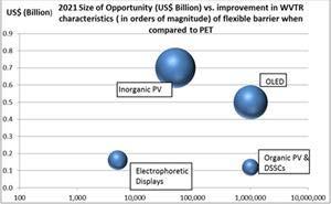
8 Ultra-barrier Market
. Total market size $23B in 2021, of which $17B are flexible OLED displays, lighting and PV. Around $1.")
9 Ultra-barrier Market The market size estimates are: 43% of the total printable and plastic electronic markets are predicted to be flexible devices requiring high grade barrier encapsulants in 2021 (IDTecEx 2012). Total market size $23B in 2021, of which $17B are flexible OLED displays, lighting and PV. Around $1.4bn for barrier products alone for flexible electronics applications in 2021 (IDTecEx 2012). BIPV flexible CIGS total market $635M by 2017 alone, with a market of $ M for clear flexible barrier films. (CIGS Photovoltaics markets-2012 report, Nanomarkets).

10 MARKET NEEDS FOR ULTRA-BARRIER
11
12 Barrier layer requirements on plastic substrates Water vapour barrier g.m 2.day -1 Polymer films 1s-100s Food packaging Electro-Chromics Flexible PV Flexible OLEDs Barrier retention over product lifetime!
13 What does this mean? ~100m ~50m Imagine a polymer sheet the size of a football pitch: How much water would pass through this over a MONTH at various barrier performance levels?


14 What does this mean? Raw Film Food Packaging OPV OLED X 1O -2 1 X 1O -4 1 X 1O -6
15 Single layer v Multilayer approach
16 Single and multi-layer barriers A key enabling technology for flexible electronics on plastic Inter-layer Barrier Barrier layer Single perfect layer Plastic film Plastic film Single layer Multi-layer Can be the substrate and encapsulation (packaging) for devices Perfect layer can provide high barrier (high density, low defects) Multi-layer approach (e.g. Vitex)
17 H 2 O (g/m 2 ) Water vapour transmission through barriers of equivalent total thickness Low barrier Time Medium barrier High barrier Single barrier Polymer H 2 O (g/m 2 ) Lag times Double barrier Time assumes dry polymer films at outset follows R.Ash et al, Brit.J.Appl.Phys see also G. Graff et al, J.Appl. Phys. 2004
18 Deposition Systems.

 In-line optical and electrical resistance monitoring Planar 10kW")
19 Optilab TM Sputter Coater micron webs Web speed m/min Plasma Treatment Medium Frequency AC dual rotatable magnetron 720mm length, 152mm Ø 6-12mm target thickness Max. 400mm web width (356mm coating width) In-line optical and electrical resistance monitoring Planar 10kW pulsed power DC magnetron 650 x 135mm target area Medium Frequency AC or pulsed DC dual planar magnetron 720mm length, 152mm Ø 6-25mm target thickness
 or rigid (Si, Glass) samples Coating is dense, with few defects relatively free of")
20 Atomic Layer Deposition (ALD) Oxford Instruments FlexALTM tool designed for processing semiconductor wafers Atomic Layer Deposition is a type of CVD process that builds up a thin film coating as a succession of layers, each ~1Ǻ thick Batch process: coating up to max 200mm wafer 140mm x 140mm Polymeric (PET, PEN) or rigid (Si, Glass) samples Coating is dense, with few defects relatively free of pinholes as required for barriers and encapsulation Different materials can be combined to form nano-scale laminates Much work taking place on continuous ALD projects
21 Barrier + Defect Measurement.
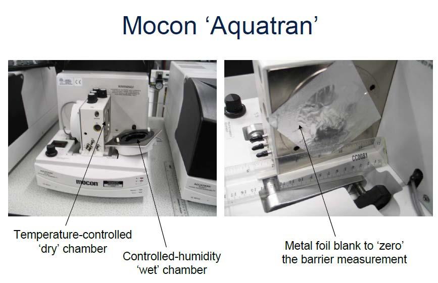
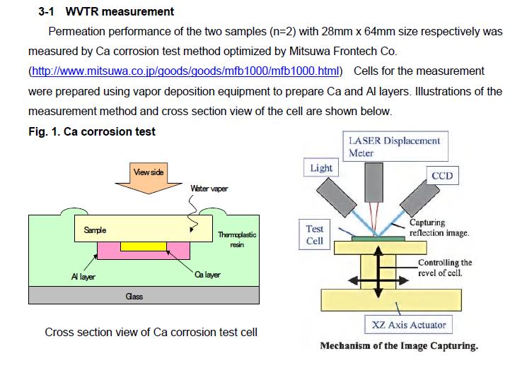
22 Barrier Measurement Mocon Water Vapour Transmission (Aquatran 1, 6 measurement stations installed) lowest sensitivity 5 x 10⁻⁴ g/m2/day calibrated standard Ca Test developing technique - issues with encapsulation - absolute measurement difficult spatial information
23 Barrier + Defect Measurements Mocon Aquatran 1Water Vapour Transmission (6 measurement stations installed) Best sensitivity 5 x 10⁻⁴ g/m2/day Calibrated standard: Quantitative Ca Test Developing technique Issues with encapsulation Absolute measurement difficult Spatial information: Qualitative Surfscan Particle Number Measurement Optical Microscopy Optical Interferometry (CCI)
24


25 PETeC Calium Test facility Class 100 Nitrogen Purged Glove Box Calcium Deposition Unit Calcium Buttons on 100mm glass slide
26 WVTR for ALD Barriers Using the Ca Test Method- Optical Measurements The sample is aged in an environmental oven and measured at intervals Is R H2O Plastic Barrier Glass A Epoxy B T Im Absorbing calcium button Camera or small-area OD meter OD meter samples ~10mm2 Camera images the 28mm dia Ca button in transmitted light Water vapour oxidises Ca metal to transparent Ca(OH) 2

27 Laser-test rig Film with colour and texture is used to show the laser beam. The transmitted beam is ~ 5 x 12 mm; the receiver slit is 1x10 mm.
28 Results on single layers, barrier and defects.
29 Sputtered Al barrier coatings Al coatings 30-60nm thick Interlayers, 2-3 micron polymer 175micron heat stabilised PET Water vapour barrier g.m 2.day -1 (Mocon) Single Al layer Double Al layer Triple Al layer < Single Al layer (non-conventional) <
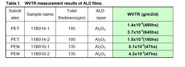
30 Comparison of layers Fast-evap AlOx -MOCON 5x10⁻¹ g/m 2 /day Sputtered AlOx (conventional) -MOCON 5x10⁻² g/m 2 /day Sputtered AlOx (non-conventional) - MOCON ~5x10⁻⁴ g/m 2 /day ALD AlOx - MOCON < 5x10⁻⁴ g/m 2 /day (meaurement conditions 38 C, 90%RH)

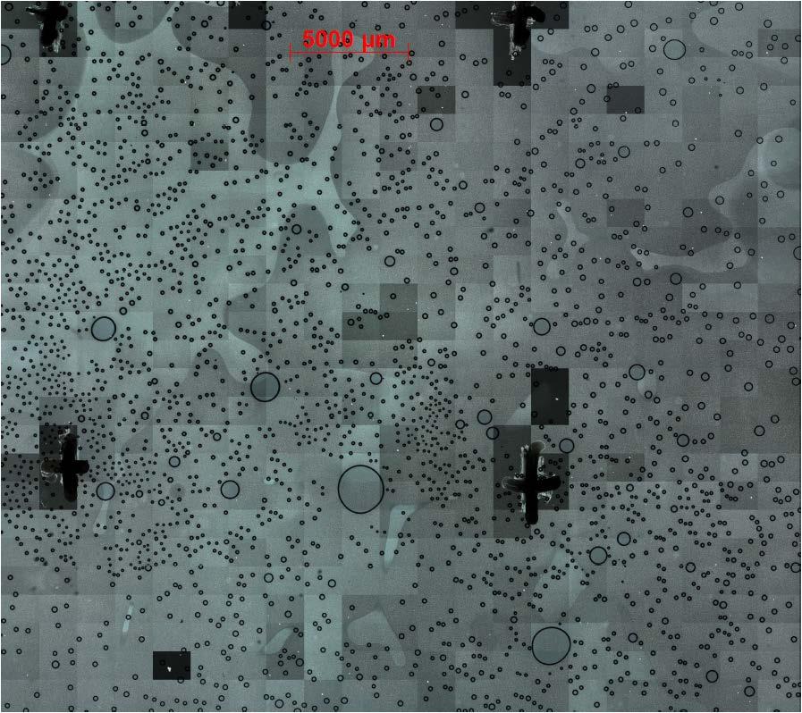
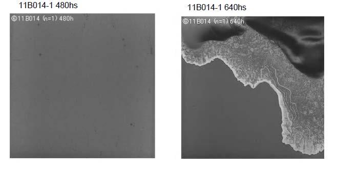
31 Defect-mapping Ca-test 30x30 mm Ca buttons on a 100x100 mm glass panel
 Failed at 3 days (21")
 Failed at 3 hours (21 C /")
32 Sputter and evap AlOx Sputter (Conventional) Failed at 3 days (21 C / 50 %RH) Fast Evap (Packaging AlOx R2R) Failed at 3 hours (21 C / 50 %RH)
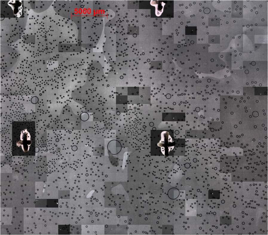
 Day 0 (60 C / 90")
33 Sputter (Non-conventional) Day -3 (21 C / 50 %RH) Day 0 (60 C / 90 %RH)
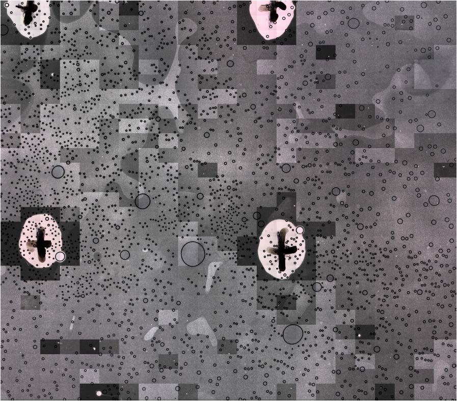
34 Sputter (Non-conventional) Day 1 (60 C / 90 %RH) Day 3 (60 C / 90 %RH)
")
 D: 0-1-3-7")
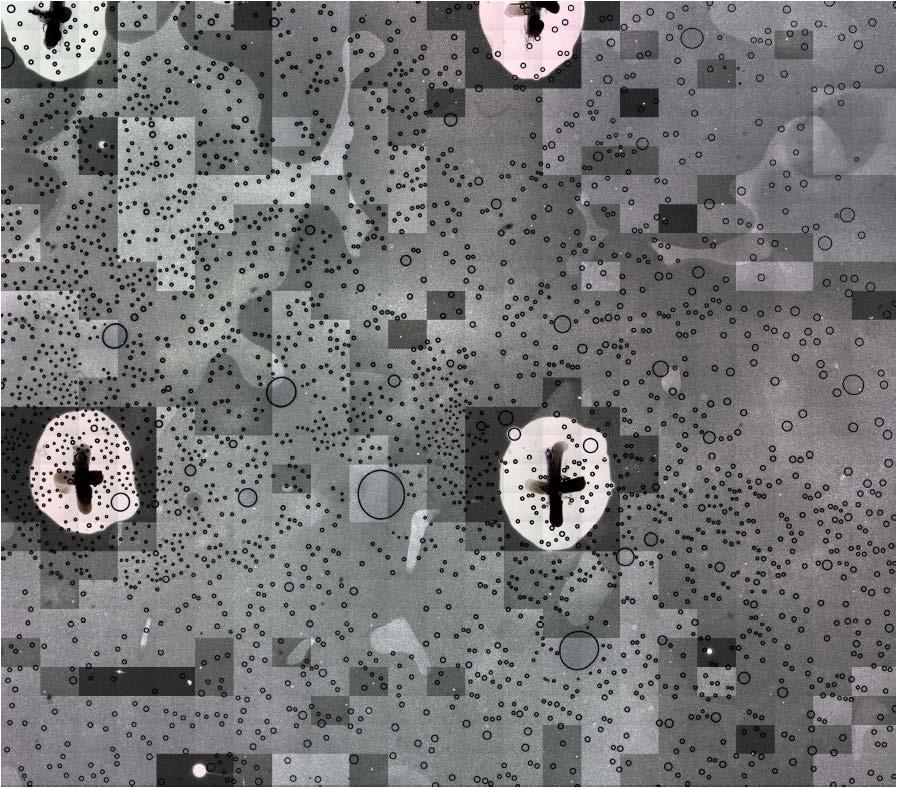
35 Sputter (Non-conventional) Day 7 (60 C / 90 %RH) D: (60 C / 90 %RH)
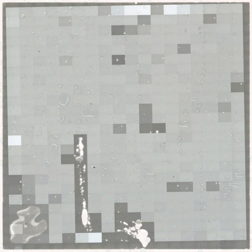
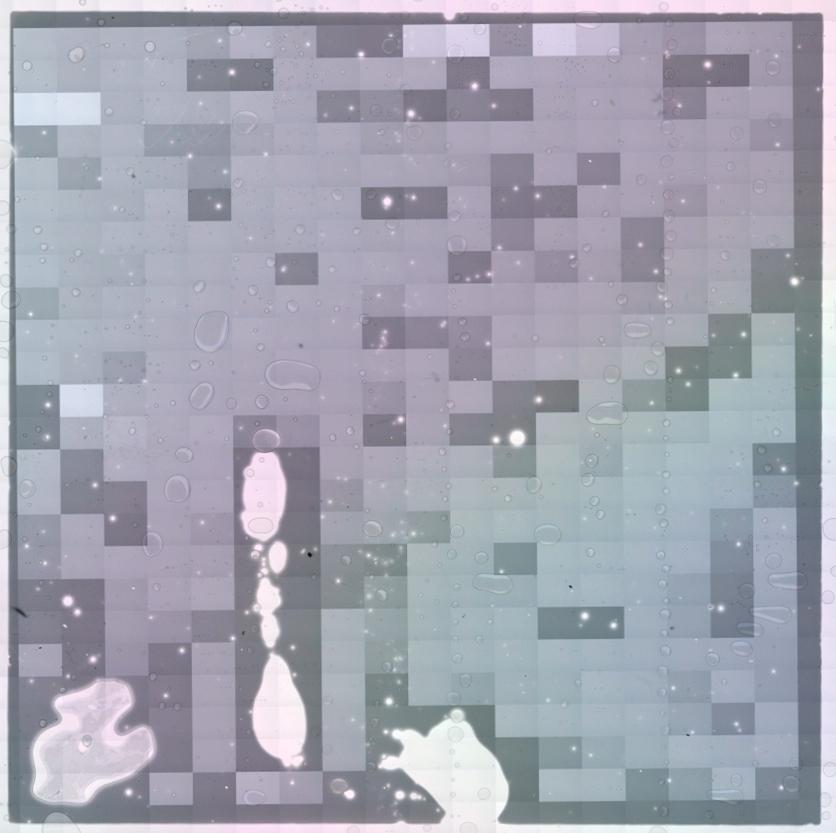
36 Y\X PPP survey x x x30 25x x20 Example of the defect count on 20x20 mm or as-received planarised PEN film x10 20x30 20x15 5x5 40x x50 10x10 30x x45 15x x30 40x x x50 40x x x x x15 50x x20 45x x40 25x20 15x25 5x x20 5x5 19 5x5 20x30 40x x80 250x200 20x30


37 ALD-Samples to compare particle counts to bright spots. Days: k2911 ALD-Feb20-03
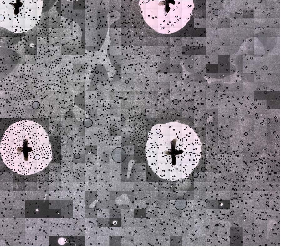
38 Comparison of particle-count defects. 12k2911 has high-barrier siblings, but low-ish particle count (~100) Particle count at µm: ALD-Feb20-03 has mediumbarrier siblings, but medium particle count (~150) Particle count at µm: The Surf-scan estimates that there are ~1 particle per square cm generated by the ALD-barrier deposition. The CCI estimates that there are 8 to 12 particles per square cm on the as-received film, which doubles on deposition. The number of bright-spots per square cm is in excess of The number of bright spots is ~50-100x the number of particle adders on reference wafers; therefore (all of) the bright spots are not caused by particles in the process. The number of bright spots is ~10x the number of as-received film defects on reference wafers; therefore (all of) the bright spots are not caused by defects in the base film. It is not known if this version of the calcium test induces defects in the barrier film. There are some bright-spot defects (e.g. 3 in 9 cm 2 ) that release as much moisture as all the rest (e.g. 900 in 9 cm 2 ) combined. The low-count/high-flow defects are the ones that must be reduced/removed.

39 Looking through the glass (and epoxy)

40 Looking through barrier film


41 Looking through the glass (and epoxy) Looking through the barrier film
42 mm Y\X P 30x20x10 1 X G 50x20 G 30x20 X X G 20x10 P 40x30 200nm G 50x X G 50x20 G 35x20 X X P 5x5 150nm 3 H 3 G 35x25 G 30x40 G 10x10 40x40x0.6 P 15x30 200nm G 35x30 G 35x30 P 25x35 P 5x5 700nm G 50x30 6 G 40x40 P 10x10 G 15x15 5 G 30x nm G 20x20 G 40x20 G 30x30 G 20x40 H 40x40 G 20x20 7 H 30x40 H 40x20 600nm G 40x70 G 10x10 G 40x30 (3micron resolution) G 40x30 Fibre 350x550 P 10x10 150nm 11 G 50x60 G 40x50 G 20x30 G 50x50 P 50x nm P 5x5 180nm H 130x nm CCI feature map X G 30x10 G 15x20 X G 3x3 G 20x15 13 X G 80x60 G 60x40 X X X G 30x30 G 10x10 14 X G 15x15 X X X G 25x15 G 25x40 15 X X G 10x30 16 G 25x20 17 G 20x15 G 20x25 G 15x15 G 30x30 18 G 35x25 G 60x G 30x30 Fibre 250x30 G 160x200 G 50x30 G 30x20 G 20x30 G 25x15 G 50x40 Fibre 500x500 G 20x20 Fibre 500x500 G 20x20 P 10x nm P 10x nm G 20x15 P 5x5 1500nm G 15x20 G 20x10 G 30x30 G 30x50 G 15x10 H 10x10 100nm G 15x25 G 15x15 P 5x5 120nm G 25x10 G 35x40 G 30x40 G 10x20 G 30x30 G 30x20 G 15x20 G 25x20 P 10x nm
43 Y\X x x x30 25x x x10 20x30 20x15 5x5 40x x50 10x10 30x x45 15x x30 40x25 Substrate surface map 14 3micron res x30 15 PPP survey x50 40x x x x x15 50x x20 45x x40 25x20 15x25 5x x20 5x5 19 5x5 20x30 40x x80 250x200 20x30
44 0hr Top, transmission
45 24hr Top, transmission
46 4days Top, transmission
47 6days Top, transmission
48 13days Top, transmission


49 CCI image of defects Large blob lower-right of lower-left cross 11-14, dot upper-right of lower-left cross

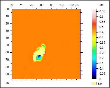
50 Attempts to ID brightening spot
51
52
53 ALD samples produced: Extrinsic barrier (large area measurement) MOCON < 5x10⁻⁴ g/m 2 /day Intrinsic barrier (small area) Laser spot 1x10⁻⁶ g/m 2 /day Excellent reproducibility at AlOx thickness >20nm Barrier for 5nm AlOX extrinsic MOCON < 5x10⁻⁴ g/m 2 /day Already produced, with lower reproducability.
54 Higher throughput ALD, towards R2R ALD.

55 Platform type CPI Batch ALD Tool (100x100mm) Present ALD - batch type Coming ALD - R2R type Present Sputter - R2R + batch type Future Combinations R2R (Sputter, ALD, etc...) CPI R2R Sputter Tool (400mm web)
56 Proposed CPI R2R ALD development Key focus for R2R ALD development: production line speeds of >1 m/min small machine footprint web width 0.5m thin high density barrier layers methods to reduce defects + effect of defects robust mechanical barrier materials low production cost
57 Technology outlook Collaboration between hardware and process development companies. Collaboration with BENEQ (Finland) Second generation system(s) currently under construction for CPI. COMING... Facilitates rapid technology engagement with industry CPI will collaborate with institutes and companies Globally for wide range application for R2R ALD. Roadmap for R2R ALD Q Scaling beyond 500 mm, line-integration Further web speed improvement by PEALD Pre-and post-processes to address particles Excellent prospects Operational to scaling to +1 meter widths, at due CPI to reasonable mechnical tolerances 0.5 mm gap across 500 mm web width

58 Beneq
59
60 Ultra-barrier Targets Line speed >5m/min Barrier 1 x 10⁻⁶ g/m 2 /day Barrier coating cost $2-4/m 2 Other coatings FUTURE as direct encapsulation (OLED, PV, PE, SENSORS) as Nano-laminates (new materials) as Contacts (work function control) as Gate dielectrics TFT devices PV structures Surface active coatings Beneq
61 Thanks for listening! Contact:
Vacuum Deposition of High Performance Gas Barrier Materials for Electronics Applications
 Vacuum Deposition of High Performance Gas Barrier Materials for Electronics Applications Hélène Suttle DPhil Research Student Department of Materials -University of Oxford AIMCAL Fall Conference October
IMRE/ETPL Flagship Project
 IMRE/ETPL Flagship Project Nanoparticulate Barrier Films & Gas Permeation Measurement Techniques for Thin Film Solar & Display Application Problems Senthil Ramadas Institute of Materials Research & Engineering
Roll-to-roll Technology for Transparent High Barrier Films
 Roll-to-roll Technology for Transparent High Barrier Films Presented at the AIMCAL Fall Technical Conference, October 19-22, 2008, Myrtle Beach, SC, USA Nicolas Schiller, John Fahlteich, Matthias Fahland,
Flexible electronics a thin film approach. Joe Pimenoff Beneq
 Flexible electronics a thin film approach Joe Pimenoff Beneq Severe semantics Thin films are thin material layers ranging from fractions of a nanometre to several micrometres in thickness. Electronic semiconductor
Nanomend Acheivements
 NANOMEND METROLOGY FOR ENHANCED NANO-SCALE DETECTION, CLEANING AND REPAIR Enhanced in-line detection, cleaning and repair of nano scale defects in thin films for flexible photovoltaic and food packaging
Future Trends in Permeation Measurement
 Future Trends in Permeation Measurement ASTM Committee FO2 Meeting Barcelona, 26-27 of September 2012 Franz Sturm LIPPKE a MOCON company This paper deals with: 1. Traditional permeation measurement needs
Progress in Roll-to-Roll Atomic Layer Deposition
 Progress in Roll-to-Roll Atomic Layer Deposition Council for Chemical Research Barrier Workshop Arlington, Virginia September 20, 2012 E. Dickey Lotus Applied Technology Outline ALD for barrier films ALD
Roll-to-roll ALD prototype for 500 mm wide webs
 Roll-to-roll ALD prototype for 500 mm wide webs Tapani Alasaarela, Mikko Söderlund, Pekka Soininen Beneq Oy, Ensimmäinen Savu, 01510 Vantaa, Finland Roll-to-roll (R2R) atomic layer deposition (ALD) technology
Manipulation and control of spatial ALD layers for flexible devices. Aimcal Memphis 2016; Edward Clerkx
 Manipulation and control of spatial ALD layers for flexible devices Meyer Burger Netherlands Equipment manufacturer Functional inkjet printing Based in Eindhoven, the Netherlands Part of world-wide Meyer
Continuous and R2R ALD for Coating of Polymer Webs
 Continuous and R2R ALD for Coating of Polymer Webs AIMCAL 2011 Web Coating Conference Dr. Mikko Söderlund Application Manager Cost of ownership [ /m 2 ] R2R ALD a paradigm change Large-area (batch) ALD
Barix Multilayers: a Water and Oxygen Barrier for Flexible Organic Electronics. Robert Jan Visser
 Barix Multilayers: a Water and Oxygen Barrier for Flexible Organic Electronics Robert Jan Visser Organic Electronics Is the Future of Electronics Organic? MIT Stanford UC Berkeley Nano Forum Vitex Systems,
Applied Research for Vacuum Web Coating: What is Coming Next?
 Applied Research for Vacuum Web Coating: What is Coming Next? Matthias Fahland, John Fahlteich, Steffen Günther, Manuela Junghähnel, Claus Luber, Nicolas Schiller, Cindy Steiner, Steffen Straach, Michiel
Transparent Ultra-Barrier Film Production and Product Integration
 Transparent Ultra-Barrier Film Production and Product Integration Mark George, Martin Rosenblum, Jason Bloking Rex Chang Vitriflex Inc., 2350 Zanker Road, Suite 20, San Jose, CA 95131 Introduction Vitriflex
Extending product lifetime with ALD moisture barrier
 Whitepaper Extending product lifetime with ALD moisture barrier 01 executive summary Atomic Layer Deposition (ALD) is a thin film technology that enables new and highly competitive products. Typical applications
ITO SPUTTER COATED FILMS FOR TOUCH PANEL APPLICATIONS USING ROTARY SINTERED CERAMIC ITO TARGETS: WHAT CAN BE LEARNED FROM GLASS COATING?
 ITO SPUTTER COATED FILMS FOR TOUCH PANEL APPLICATIONS USING ROTARY SINTERED CERAMIC ITO TARGETS: WHAT CAN BE LEARNED FROM GLASS COATING? Paul Lippens AIMCAL Web coating conference 2012 Outline Introduction
Barrier Films and Adhesives for Display Applications CCR OLED Workshop, June 8, 2011, U of MN
 Barrier Films and Adhesives for Display Applications CCR OLED Workshop, June 8, 2011, U of MN 3M Company Overview Sales: $23.1 B Net income: $3.2 B R&D investment $1.3 B (5.6% to sales) International sales
Vacuum Deposition of High Performance Gas Barrier Materials
 Vacuum Deposition of High Performance Gas Barrier Materials H. Suttle, A. J. Topping, & H. E. Assender Department of Materials, University of Oxford, Parks Road, Oxford OX1 3PH ABSTRACT High performance
Nanoscale Barrier Coating on BOPP Packaging Film by ALD Presented by: Dr. Johanna Lahti Senior Research Fellow Tampere University of Technology
 Nanoscale Barrier Coating on BPP Packaging Film by ALD Presented by: Dr. Johanna Lahti Senior Research Fellow Tampere University of Technology Co-authors: Kimmo Lahtinen (LUT*), Petri Johansson (TUT),
AIMCAL R2R Conference
 Contents Introduction Markets OLED Structures Technology Fabrication Process Evaluation (Microstructure & etc) Summary Introduction [Merit of Rigid OLED Display] Cheap product cost Mass production Free
Bringing Permeation Barrier Technology to Application. From Ultra-High Barrier Films to Functional Films for Flexible Electronics
 Bringing Permeation Barrier Technology to Application From Ultra-High Barrier Films to Functional Films for Flexible Electronics Degradation of organic devices on plastic films Barrier layer stack 1 1
University of Huddersfield Repository
 University of Huddersfield Repository Elrawemi, Mohamed, Blunt, Liam, Fleming, Leigh, Sweeney, Francis and Robbins, David Defect Detection in Thin-film Photovoltaics; Towards Improved Efficiency and Longevity
Photovoltaics & Solar Thermals. Thin-film equipment. Customized. FHR Anlagenbau GmbH I
 Photovoltaics & Solar Thermals Thin-film equipment. Customized. FHR Anlagenbau GmbH I www.fhr.de FHR Anlagenbau GmbH is an innovative enterprise in the branch of vacuum processing and thin-film technologies.
Improvement of gas barrier properties by combination of polymer film and gas barrier layer
 Improvement of gas barrier properties by combination of polymer film and gas barrier Y. Tsumagari, H. Murakami, K. Iseki and S. Yokoyama Toyobo Co., LTD. RESEARCH CENTER, - Katata 2-chome, Otsu, Shiga,
Laser Micromachining of Bulk Substrates and Thin Films Celine Bansal
 Laser Micromachining of Bulk Substrates and Thin Films Celine Bansal Oxford Lasers Ltd Moorbrook Park Didcot, Oxfordshire, OX11 7HP Tel: +44 (0) 1235 810088 www.oxfordlasers.com Outline Oxford Lasers Importance
New Surface Properties by Atomic Layer Deposition
 New Surface Properties by Atomic Layer Deposition Beneq Oy, Finland Dr Tommi Vainio, CTO HANNOVER MESSE MicroTechnology Forum Innovations for Industry April 21, 2009 Turning Innovations into Success 1
Enabling new industries with high volume manufacturing: learnings from R2R processing in wearable and flexible displays
 Enabling new industries with high volume manufacturing: learnings from R2R processing in wearable and flexible displays Tobias Stolley, Technologist Applied Materials WEB Coating GmbH Industiral Technologies
Samuel Graham. Acknowledgements
 Development of Barrier Films for Packaging Flexible Electronics Samuel Graham Woodruff School of Mechanical Engineering School of Materials Science and Engineering Center for Organic Photonics and Electronics
Further Development of Surface Metrology Methods for Predicting the Functional Performance of Flexible PV Barrier Films
 Further Development of Surface Metrology Methods for Predicting the Functional Performance of Flexible PV Barrier Films M Elrawemi 1, L Blunt 1, L Fleming 1 and F Sweeney 1 1 University of Huddersfield,
Flexible functional devices at mass production level with the FLEx R2R sald platform
 Flexible functional devices at mass production level with the FLEx R2R sald platform D. Spee, W. Boonen, D. Borsa and E. Clerkx Meyer Burger (Netherlands) B.V. Meyer Burger Introduction to sald Challenges
Vacuum Coating Process Issues for Photovoltaic Devices
 Vacuum Coating Process Issues for Photovoltaic Devices James R. Sheats Lost Arrow Consulting Palo Alto, CA sheats@lostarrowc.com * AIMCAL Fall Conference (Vacuum Web Coating), Charleston, S.C. 25 October
Roll-to-roll Vacuum Processing of Organic Thin Film Transistors
 Roll-to-roll Vacuum Processing of Organic Thin Film Transistors Hazel Assender Department of Materials University of Oxford DALMATIAN TECHNOLOGY 1 Aim of the Research To demonstrate the ability to fabricate
Solar Film Introduction. Company Presentation 1
 olar Film Introduction Company Presentation 1 Executive ummary Background pecialized in the production of organic solar films based on proprietary IP Founded in 2006 out of two leading universities HQ
ALD Atomic Layer Deposition
 ALD Atomic Layer Deposition Christophe Vallée Laboratoire des Technologies de la Microélectronique (LTM) Univ. Grenoble Alpes, Lab. LTM (CEA-LETI/MINATEC) - Grenoble France christophe.vallee@cea.fr 1.
CONFERENCE EVALUATION FORM
 2015 AIMCAL Web Coating & Handling / SPE FlexPackCon CONFERENCE EVALUATION FORM To upgrade the quality of the Web Coating & Handling / FlexPackCon Conference, we would appreciate your comments. MONDAY,
Mass Production of Clear Barriers. Requirements on Vacuum Web Coaters for Quality Assurance. Rainer Ludwig, Applied Films, Alzenau, Germany.
 Mass Production of Clear Barriers Requirements on Vacuum Web Coaters for Quality Assurance Rainer Ludwig, Applied Films, Alzenau, Germany Abstract An increasing number of packages using Transparent Barrier
Atomic Layer Deposition
 Atomic Layer Deposition Ville Malinen R&D Engineer Nanopinnoitteita koneenrakentajille 2010 1 Introduction 1) Overview of Beneq 2) Atomic Layer Deposition (ALD), to deposit thin films, which Are dense
Gencoa Product Portfolio
 Gencoa offer the following range of products & process technology for the thin film industry developed over the last 20 years Planar Magnetrons Plasma Pre- Treaters Reactive Gas Controllers Gencoa Product
Roll-to-Roll ALD Deposition of Al 2 O 3 Barrier Layers on PET
 Roll-to-Roll ALD Deposition of Al 2 O 3 Barrier Layers on PET W. A. Barrow and E. R. Dickey Lotus Applied Technology AIMCAL Fall Technical Conference 2009 Amelia Island Plantation, Florida 20-Oct-2009
EFFICIENCY AND PRODUCTIVITY INCREASE OF SOLAR-CELLS AND -MODULES BY INNOVATIVE LASER APPROACHES
 EFFICIENCY AND PRODUCTIVITY INCREASE OF SOLAR-CELLS AND -MODULES BY INNOVATIVE LASER APPROACHES PD Dr. Alexander Horn, V. Schütz, J. Gonzalez, C.C. Kalmbach Photovoltaics Group Dpt. for Production and
VISION INNOVATE INSPIRE DELIVER
 INSPIRE Vision About NovaCentrix Photonic Curing INNOVATE History Applications DELIVER Our Products SimPulse Conductive Inks NanoPowders VISION NovaCentrix partners with you to take ideas from inspiration
Electronics from the Printing Press
 Electronics from the Printing Press Hannover Messe 2011 April 4 8, 2011, Hannover Research & Technology Leading Trade Fair for R & D and Technology Transfer Hall 2, Booth C18 Research Teaching Innovation
High Rate low pressure PECVD for barrier and optical coatings
 High Rate low pressure PECVD for barrier and optical coatings, Matthias Fahland, John Fahlteich, Björn Meyer, Steffen Straach, Nicolas Schiller Outline Introduction PECVD New developments magpecvd arcpecv
Copper Interconnect Technology
 Tapan Gupta Copper Interconnect Technology i Springer Contents 1 Introduction 1 1.1 Trends and Challenges 2 1.2 Physical Limits and Search for New Materials 5 1.3 Challenges 6 1.4 Choice of Materials 7
High Barrier Multi-Layer Parylene Coating
 High Barrier Multi-Layer Parylene Coating Technology overview Surface Technolgy 2018 Company Profile Swiss company founded in 1979 Experts in Parylene coating technology Parylene Equipment Export rate
Aluminum oxide barrier layers on polymer web
 Aluminum oxide barrier layers on polymer web Carolin Struller PhD research student Manchester Metropolitan University Bobst Manchester (formerly General Vacuum Equipment) Peter Kelly, Nick Copeland, Chris
"ITO Film Trend for Touch Panel Applications"
 AIMCAL Web Coating Conference 2011 October 23-26 Reno, Nevada USA 1 "ITO Film Trend for Touch Panel Applications" Teijin Chemicals Ltd. Haruhiko Itoh 2 Content 1. Structure and Features of TCF 2. Touch
Simultaneous Multilayer Coating for Batteries
 Simultaneous Multilayer Coating for Batteries Enabling higher performance at reduced cost through processing innovation Page 1 Multilayer Coating Value Proposition Simultaneous Multilayer Coating (MLC)
Barrier Coating Encapsulation Using Rotatable Cylindrical Sputtering Cathodes
 Barrier Coating Encapsulation Using Rotatable Cylindrical Sputtering Cathodes V. Bellido-Gonzalez, D. Monaghan, R. Brown, B. Daniel, J. Brindley, A. Azzopardi, and I. Sorzabal-Bellido, Gencoa Ltd., Liverpool,
Comparison of Different Sputter Processes for ITO: Planar DC versus Planar AC
 Comparison of Different Sputter Processes for ITO: Planar DC versus Planar AC P. Sauer, H.-G. Lotz, A. Hellmich, R. Kukla, J. Schröder Applied Films GmbH & Co. KG, Alzenau, Germany Key Words: ITO MF PET
AIMCAL EUROPE WEB COATING CONFERENCE-PRAGUE JUNE 2012
 AIMCAL EUROPE WEB COATING CONFERENCE-PRAGUE 11-13 JUNE 212 Gas Barrier Coatings for Flexible Packaging 1. Introduction Having investigated the evolution of barrier technologies in packaging, it became
ADDING VALUE TO VACUUM COATED PRODUCTS BY IMPROVING METALLIZED FILMS PROPERTIES AND FUNCTIONALITIES
 ADDING VALUE TO VACUUM COATED PRODUCTS BY IMPROVING METALLIZED FILMS PROPERTIES AND FUNCTIONALITIES by Fabiano Rimediotti NORMECCANICA GROUP Vacuum Division Piacenza Italy OUTLINE Introduction - Motivation
ROLL TO ROLL FABRICATION PROCESS OF THIN FILM SILICON SOLAR CELLS ON STEEL FOIL
 ROLL TO ROLL FABRICATION PROCESS OF THIN FILM SILICON SOLAR CELLS ON STEEL FOIL B.B. Van Aken, M. Dörenkämper, C. Devilee, M.C.R. Heijna, J. Löffler and W.J. Soppe ECN Solar Energy, P.O. Box 1, 1755 ZG
Amorphous Oxide Transistor Electrokinetic Reflective Display on Flexible Glass
 Amorphous Oxide Transistor Electrokinetic Reflective Display on Flexible Glass Devin A. Mourey, Randy L. Hoffman, Sean M. Garner *, Arliena Holm, Brad Benson, Gregg Combs, James E. Abbott, Xinghua Li*,
High Performance Barrier Films for Vacuum Insulation Panels Abstract Background 3M Barrier Film
 High Performance Barrier Films for Vacuum Insulation Panels Cedric Bedoya, Christopher Lyons, Kim Pollard, Don McClure, Scott J. Jones, 3M Corporate Research Lab, St. Paul, Minnesota, USA Paul Engen, Matt
Aluminum oxide barrier coatings on polymeric substrates
 Aluminum oxide barrier coatings on polymeric substrates Carolin Struller PhD research student Manchester Metropolitan University, Bobst Manchester Ltd. Nick Copeland Bobst Manchester Ltd. Peter Kelly,
Magnetron Sputter Cathodes planar & rotatable. Linear ion sources. Reactive gas controller & endpoint detector
 GENCOA products cover 3 sputtering related areas Magnetron Sputter Cathodes planar & rotatable Reactive gas controller & endpoint detector Linear ion sources Other activities include on-site process implementation,
High Rate Deposition of Reactive Oxide Coatings by New Plasma Enhanced Chemical Vapor Deposition Source Technology
 General Plasma, Inc. 546 East 25th Street Tucson, Arizona 85713 tel. 520-882-5100 fax. 520-882-5165 High Rate Deposition of Reactive Oxide Coatings by New Plasma Enhanced Chemical Vapor Deposition Source
EQUIPMENT EQUIPMENT FOR HIGH-EFFICIENCY SOLAR CONCEPTS CRYSTALLINE SILICON PV. SCALA XEA nova XENIA
 CRYSTALLINE SILICON PV EQUIPMENT EQUIPMENT FOR HIGH-EFFICIENCY SOLAR CONCEPTS SCALA XEA nova XENIA VON ARDENNE was founded in 1991 as a spin-off of the former Manfred von Ardenne Research Institute. The
Plasma Activated EB-PVD of Titanium and its Compounds by Means of Large Area SAD
 AIMCAL 2005 Myrtle Beach, SC, USA, October 19th, 2005 Plasma Activated EB-PVD of Titanium and its Compounds by Means of Large Area SAD E. Reinhold, C. Steuer VON ARDENNE Anlagentechnik GmbH, Dresden, Germany
EECS130 Integrated Circuit Devices
 EECS130 Integrated Circuit Devices Professor Ali Javey 9/13/2007 Fabrication Technology Lecture 1 Silicon Device Fabrication Technology Over 10 15 transistors (or 100,000 for every person in the world)
VCF Films. superior thin film. solutions for highly. engineered products
 VCF Films superior thin film solutions for highly engineered products From solar panels to medical probes, thin films are revolutionizing a wide range of industries and fueling new innovations around the
EXCIMER LASER ANNEALING FOR LOW- TEMPERATURE POLYSILICON THIN FILM TRANSISTOR FABRICATION ON PLASTIC SUBSTRATES
 EXCIMER LASER ANNEALING FOR LOW- TEMPERATURE POLYSILICON THIN FILM TRANSISTOR FABRICATION ON PLASTIC SUBSTRATES G. Fortunato, A. Pecora, L. Maiolo, M. Cuscunà, D. Simeone, A. Minotti, and L. Mariucci CNR-IMM,
Atomic Oxygen-Resistant, Static-Dissipative, Pinhole-Free Coatings for Spacecraft
 Physical Sciences Inc. VG10-109 Atomic Oxygen-Resistant, Static-Dissipative, Pinhole-Free Coatings for Spacecraft Michelle T. Schulberg, Robert H. Krech, Frederick S. Lauten Physical Sciences Inc. Roy
Future Thin and Flexible Systems?
 Packaging and Thermal Management Challenges for Future 1-mm Thin Smartphones? Y. C. Lee, University of Colorado - Boulder Three CU technologies: Flexible thermal ground planes All solid state battery Atomic
Developing Enhanced Substrates for OLED SSL
 Developing Enhanced Substrates for OLED SSL DOE SSL R&D Manufacturing Workshop San Diego CA 7 May, 2014 Dr. W. Dennis Slafer MicroContinuum, Inc. 57 Smith Place Cambridge, MA 02138 www.microcontinuum.com
Ultra High Barrier Coatings by PECVD
 Society of Vacuum Coaters 2014 Technical Conference Presentation Ultra High Barrier Coatings by PECVD John Madocks & Phong Ngo, General Plasma Inc., 546 E. 25 th Street, Tucson, Arizona, USA Abstract Silicon
Advanced Sheet-to-Sheet and Roll-to-Roll thin-film processing on ultra-thin flexible glass for flexible electronic devices
 Advanced Sheet-to-Sheet and Roll-to-Roll thin-film processing on ultra-thin flexible glass for flexible electronic devices M. Junghaehnel 1, J. Westphalen 1, F. Naumann 2, G. Lorenz 2, M. Fahland 1, S.
Challenges and Future Directions of Laser Fuse Processing in Memory Repair
 Challenges and Future Directions of Laser Fuse Processing in Memory Repair Bo Gu, * T. Coughlin, B. Maxwell, J. Griffiths, J. Lee, J. Cordingley, S. Johnson, E. Karagiannis, J. Ehrmann GSI Lumonics, Inc.
Advanced Glass Refinement by Thin Films - Trends and Challenges of Thin Film Technologies for Windows and Facade Glasses
 Advanced Glass Refinement by Thin Films - Trends and Challenges of Thin Film Technologies for Windows and Facade Glasses Dr.-Ing. Manuela Junghähnel Fraunhofer Institute for Elect ron Beam and Plasma Technology
TOWARDS FLEXIBLE ENCAPSULATED PLASTIC ELECTRONICS. Christina Schinagl Dresden, 9 th October 2012
 TOWARDS FLEXIBLE ENCAPSULATED PLASTIC ELECTRONICS Christina Schinagl Dresden, 9 th October 2012 OVERVIEW Company Introduction Backsheets and Encapsulants for PV Flexible Electronics Fronsheet Barrier Material
Thin Films: Sputtering Systems (Jaeger Ch 6 & Ruska Ch 7,) Can deposit any material on any substrate (in principal) Start with pumping down to high
 Can deposit any material on any substrate (in principal) Start with pumping down to high") Thin Films: Sputtering Systems (Jaeger Ch 6 & Ruska Ch 7,) Can deposit any material on any substrate (in principal) Start with pumping down to high vacuum ~10-7 torr Removes residual gases eg oxygen from
Thin Films: Sputtering Systems (Jaeger Ch 6 & Ruska Ch 7,) Can deposit any material on any substrate (in principal) Start with pumping down to high vacuum ~10-7 torr Removes residual gases eg oxygen from
AIMCAL Fall Technical Conference & 19th International Conference on Vacuum Web Coating
 AIMCAL Fall Technical Conference & 19th International Conference on Vacuum Web Coating A.G. Talma, R. Schlatmann, J.W.G. Mahy Akzo Nobel Chemicals bv, P.O. Box 9300, 6800 SB Arnhem, The Netherlands. Phone
R&D ACTIVITIES AT ASSCP-BHEL,GURGAON IN SOLAR PV. DST-EPSRC Workshop on Solar Energy Research
 R&D ACTIVITIES AT -BHEL,GURGAON IN SOLAR PV at the DST-EPSRC Workshop on Solar Energy Research (22 nd 23 rd April, 2009) by Dr.R.K. Bhogra, Addl. General Manager & Head Email: cpdrkb@bhel.co.in Dr.A.K.
Laser Crystallization for Low- Temperature Poly-Silicon (LTPS)
") Laser Crystallization for Low- Temperature Poly-Silicon (LTPS) David Grant University of Waterloo ECE 639 Dr. Andrei Sazonov What s the current problem in AM- LCD and large-area area imaging? a-si:h has
Laser Crystallization for Low- Temperature Poly-Silicon (LTPS) David Grant University of Waterloo ECE 639 Dr. Andrei Sazonov What s the current problem in AM- LCD and large-area area imaging? a-si:h has
More on VLSI Fabrication Technologies. Emanuele Baravelli
 More on VLSI Fabrication Technologies Emanuele Baravelli Some more details on: 1. VLSI meaning 2. p-si epitaxial layer 3. Lithography 4. Metallization 5. Process timings What does VLSI mean, by the way?
LOT. Contents. Introduction to Thin Film Technology. Chair of Surface and Materials Technology
 Introduction to Thin Film Contents 1. Introduction and Application Examples (2h) 2. Preparation of Thin Films by PVD (Physical Vapor Deposition) (6h) 2.1 Vacuum Technique (1h) 2.1.1 Kinetics of Gases 2.1.2
Chapter 3 Silicon Device Fabrication Technology
 Chapter 3 Silicon Device Fabrication Technology Over 10 15 transistors (or 100,000 for every person in the world) are manufactured every year. VLSI (Very Large Scale Integration) ULSI (Ultra Large Scale
Atomic Layer Deposition. ALD process solutions using FlexAL and OpAL
 Atomic Layer Deposition process solutions using FlexAL and OpAL Introduction to Self limiting digital growth Atomic Layer Deposition () offers precisely controlled ultra-thin films for advanced applications
FRAUNHOFER INSTITUTE FOR SURFACE ENGINEERING AND THIN FILMS IST OPTICAL COATINGS
 FRAUNHOFER INSTITUTE FOR SURFACE ENGINEERING AND THIN FILMS IST OPTICAL COATINGS OPTICAL FUNCTIONAL COATINGS AT THE FRAUNHOFER IST The development of optical functional films and the related coating processes
Production of PV cells
 Production of PV cells MWp 1400 1200 Average market growth 1981-2003: 32% 2004: 67% 1000 800 600 400 200 0 1991 1992 1993 1994 1995 1996 1997 1998 1999 2000 2001 2002 2003 2004 rest 1.0 1.0 1.0 2.0 4.0
Market Trends, Opportunities and Latest Process Innovation in Vacuum Metallization Introducing BOBST AluBond Technology
 Market Trends, Opportunities and Latest Process Innovation in Vacuum Metallization Introducing BOBST AluBond Technology Nick Copeland, Bobst Manchester Ltd Carolin Struller, Bobst Manchester Ltd AIMCAL
Development of Conductive Polymer Film and R2R Coating Process
 Development of Conductive Polymer Film and R2R Coating Process Nizamidin Jappar; Ph.D. General Manager of R&D Kimoto Tech Inc. AIMCAL Web Coating & Handling Conference Outline 1 Background 2 3 4 Develop
The Potential of Photovoltaics
 The Potential of Photovoltaics AIMCAL 2008 2008 Fall Conference Vacuum Web Coating Brent P. Nelson October 22, 2008 NREL is a national laboratory of the U.S. Department of Energy Office of Energy Efficiency
Vacuum Equipment for TCO and AR Coatings Deposition by Reactive Magnetron Sputtering
 Vacuum Equipment for TCO and AR Coatings Deposition by Reactive Magnetron Sputtering E. Yadin; V. Kozlov; E. Machevskis, Sidrabe, Inc., 17 Krustpils str.,riga, LV1073, Latvia. Tel: +371 7249806, Fax: +371
Roll-to-Roll Nanoimprint - 6 회 -
 Roll-to-Roll Nanoimprint - 6 회 - 목차 Click to add Title 1 Roll to Roll nanoimprint Introduction : Continuous Production System (Roll-to-Roll) Fabrication Processes Fabrication of nano roll mold 2 Case study
On the way to the latest packaging R2R Metallizer
 On the way to the latest packaging R2R Metallizer AIMCAL FALL Conference 2011 Schmid Vacuum Technology GmbH, Karlstein, Germany Peter Sauer Gerard Löbig Andre Herzog Johannes Krantz Michael Klosch-Trageser
MICROFABRICATION OF OPTICALLY ACTIVE InO X MICROSTRUCTURES BY ULTRASHORT LASER PULSES
 Journal of Optoelectronics and Advanced Materials Vol. 4, No. 3, September 2002, p. 809-812 MICROFABRICATION OF OPTICALLY ACTIVE InO X MICROSTRUCTURES BY ULTRASHORT LASER PULSES Foundation for Research
Low temperature deposition of thin passivation layers by plasma ALD
 1 Low temperature deposition of thin passivation layers by plasma ALD Bernd Gruska, SENTECH Instruments GmbH, Germany 1. SENTECH in brief 2. Low temperature deposition processes 3. SENTECH SI ALD LL System
Your ideas. Our technologies.
 Your ideas. Our technologies. For more than a decade, 3M has been a trusted supplier of advanced materials for the solar industry. Our broad range of products and technologies is designed to enhance performance,
Microsystem Integration (March 20, 2017)
") Microsystem Integration (March 20, 2017) Mid-term exam: open notes/computers/ - 1:00 to 1:50 p.m., Wednesday, March 22. Homeworks #1 to 7. - Solutions of #1 to 7 are posted. Workshops #1 to 15. - Workshops
Microsystem Integration (March 20, 2017) Mid-term exam: open notes/computers/ - 1:00 to 1:50 p.m., Wednesday, March 22. Homeworks #1 to 7. - Solutions of #1 to 7 are posted. Workshops #1 to 15. - Workshops
SolarWindow. Innovating Alternative and Renewable Energy Solutions. Corporate» Technology» Media» Investors» Contact
 Innovating Alternative and Renewable Energy Solutions A A A Corporate» Technology» Media» Investors» Contact SolarWindow New Energy Technologies is developing the first-of-its kind SolarWindow technology,
Nucleation and growth of nanostructures and films. Seongshik (Sean) Oh
 Oh") Nucleation and growth of nanostructures and films Seongshik (Sean) Oh Outline Introduction and Overview 1. Thermodynamics and Kinetics of thin film growth 2. Defects in films 3. Amorphous, Polycrystalline
Nucleation and growth of nanostructures and films Seongshik (Sean) Oh Outline Introduction and Overview 1. Thermodynamics and Kinetics of thin film growth 2. Defects in films 3. Amorphous, Polycrystalline
Linear Plasma Sources for Surface Modification and Deposition for Large Area Coating
 Linear Plasma Sources for Surface Modification and Deposition for Large Area Coating Dr Tony Williams Gencoa Ltd, UK Victor Bellido-Gonzalez, Dr Dermot Monaghan, Dr Joseph Brindley, Robert Brown SVC 2016,
Research and demonstration in the area of nanotechnology and packaging materials
 Research and demonstration in the area of nanotechnology and packaging materials 1 TAMPERE UNIVERSITY OF TECHNOLOGY (TUT) Established in 1965, started operating in the form of a foundation in 2010 The
Q150R Series Rotary Pumped Coaters
 Q u o r u m Te c h n ologies Q150R Modular Coating Systems Q Series Rotary Pumped Coating Systems Innovative and versatile sputter High vacuum sputtering and carbon coater and carbonfor evaporator evaporation
PHS6317 NANO-ENGINEERING OF THIN FILMS
 PHS6317 NANO-ENGINEERING OF THIN FILMS Ludvik Martinu, ing., PhD Professor Chairholder: NSERC Multisectorial Industrial Research Chair in Coatings and Surface Engineering ludvik.martinu@polymtl.ca www.polymtl.ca/larfis
Productivity versus Profitability in Vacuum Web Coating
 Productivity versus Profitability in Vacuum Web Coating Liz Josephson, Applied Films Corp., Longmont, USA Dirk Hoffmann, Applied Films GmbH & Co KG, Alzenau, Germany Gerard Loebig, Applied Films GmbH &
Innovative Roll-to-Roll Equipment & Material Development Suite
 Innovative Roll-to-Roll Equipment & Material Development Suite For Next Generation Technology from Carpe Diem Technologies and the University of Massachusetts Amherst By John Berg, Dimitur Benchev, James
SINGULUS TECHNOLOGIES. SINGULUS TECHNOLOGIES AG _ Q1 Presentation
 SINGULUS TECHNOLOGIES _ Q1 Presentation May 2017 Agenda May 12, 2017-2 - 1 Overview 2 Financials 3 SINGULUS TECHNOLOGIES Segments & New Business Areas 4 SINGULUS TECHNOLOGIES Outlook SINGULUS TECHNOLOGIES
Challenges of Fan-Out WLP and Solution Alternatives John Almiranez
 Challenges of Fan-Out WLP and Solution Alternatives John Almiranez Advanced Packaging Business Development Asia Introduction to Fan-Out WLP Introduction World of mobile gadgetry continues to rapidly evolve