Plasmons. Surface Plasmon Resonance. Plasmonic Effects and Applications
|
|
|
- Alexandrina Pitts
- 6 years ago
- Views:
Transcription
1 Plasmons Surface Plasmon Resonance Plasmonic Effects and Applications
2 Introduction During the last two decades many researches devoted to develop optical sensors for the measurement of chemical and biological quantities. In the beginning, the optical chemical sensors were based on the measurement of changes in absorption spectrum and were developed for the measurement of CO 2 and O 2 concentrations. Since then, a large variety of optical methods have been used in chemical and biosensors, among them, Surface Plasmon Resonance. In these sensors, a desired quantity is determined by measuring the refractive index, absorbance and fluorescence properties of analyte molecules.
3 Introduction Plasmon: The quanta of waves produced by collective effects of large numbers of electrons in matter when the electrons are disturbed from equilibrium. The quantum of Plasma Oscillation is called Plasmon Metals provide the best evidence of plasmons, because they have a high density of electrons free to move. The name plasmon derives from the physical plasma as a state of matter in which the atoms are ionized. At the lowest densities this means an ionized gas, or classical plasma; but densities are much higher in a metal, the atoms of a solid metal being in the form of ions. In both types of physical plasma, the frequency of plasmawave oscillation is determined by the electronic density. In a quantum plasma the energy of the plasmon is its frequency multiplied by Planck's constant, a basic relationship of quantum mechanics.
4 Introduction Plasmons play a large role in the optical properties of metals. Light of frequency below the plasma frequency is reflected, because the electrons in the metal screen the electric field of the light. Light of frequency above the plasma frequency is transmitted, because the electrons cannot respond fast enough to screen it. In most metals, the plasma frequency is in the ultraviolet, making them shiny (reflective) in the visible range. On the other hand, some metals, such as copper, have a plasmon frequency in the visible range, yielding their distinct color. The geometry of the metal film plays an important role in plasmon frequency. For example gold, has plasmon frequency in the deep ultraviolet, but geometric factors bring it close to the visible. In doped semiconductors, the plasma frequency is usually in the infrared.

5 Introduction High interest of artists regarding scattering absorption of light from noble metal nanoparticles source of colors in stained glass windows even before scientifically investigated. Sizes, shapes, and compositions of metal nanoparticles can be systematically varied to produce materials with distinct lightscattering properties. 5
6 Introduction The plasmon energy for most metals corresponds to that of an ultraviolet photon. However, as mentioned above for some metals like silver, gold, the alkali metals, and a few other materials, the plasmon energy can be sufficiently low to correspond to that of a visible or near-ultraviolet photon. This means there is a possibility of exciting plasmons by light. If plasmons are confined upon a surface, optical effects can be easily observed. In this case, the quanta are called surface plasmons, SP, and they have the bulk plasmon energy as an upper energy limit. Surface plasmons were first proposed to explain energy losses by electrons reflected from metal surfaces. Since then, numerous experiments have involved coupling photons to surface plasmons. Potential applications extend to new light sources, solar cells, holography, Raman spectroscopy, microscopy, and sensors.
7 Introduction Surface plasmons are those plasmons that are confined to surfaces and that interact strongly with light resulting in a polariton, SPP. They occur at the interface of a material with a positive dielectric constant with that of a negative dielectric constant (usually a metal or doped dielectric).
8 Introduction Surface plasmons on a plane surface are nonradiative electromagnetic modes, that is, SPP cannot be generated directly by light nor can they decay spontaneously into photons. The origin of the non-radiative nature of SPP is that the interaction between light and SP cannot simultaneously satisfy energy and momentum conservation. This restriction can be circumvented by relaxing the momentum conservation requirement by roughening or corrugating the metal surface. Other method is to increase the effective wave vector (and hence momentum) of the light by some means (discussed later).
9 Surface Plasmon Resonance The excitation of surface plasmons by light is denoted as a surface plasmon resonance (SPR) for planar surfaces or localized surface plasmon resonance (LSPR) for nanometer-sized metallic structures. Surface plasmon polaritons (SPP), ( coupling between photon and an excitation of a material) are surface electromagnetic waves that propagate parallel along a metal/dielectric interface. For surface plasmons to exist, the complex dielectric constants of the two media must be of opposite sign. This condition is met in the IR-visible wavelength region for air/metal and water/metal interfaces (where the real dielectric constant of a metal is negative and that of air or water is positive). Typical metals that support surface plasmons are silver and gold, but metals such as copper, titanium, or chromium can also support surface plasmon generation.


10 Surface Plasmon and Localized Surface Plasmon Resonance Surface Plasmon (SP): Charge density wave that exists at the interface between metal and dielectric - Plasmons propagate along metal dielectric interface Excitation of SP: momentum of incident photon = that of plasmon resonance Sensing; measurement of absorption: function of angle of incidence or function λ (we used the latter) Light at certain λ causes conduction electrons oscillate around the nanoparticles LSPR is similar to SPR but it is localized refers to the frequency at which plasmons oscillate around the nanoparticle or when light is in resonance with collective oscillation of electrons Sensing; measurement of absorption: function of angle of incidence or function λ (we used the latter)
 ym ( E,0, E )exp i( k x k z t) xm zm xm xm zm zm Maxwell s equation in the medium i ( i = metal or dielectric ) H E i t i H i E E t 0 i H 0 0 At the boundaries E x, m Ex, d mezm d Ezd H y, m")
11 Derivation of dispersion relation of Surface Plasmon Polaritons Dielectric Metal H E d d ( 0, H,0)exp i( k x k z t) yd Z>0 Z<0 ( E,0, E )exp i( k x k z t) xd zd xd xd zd zd E H m m ( 0, H,0)exp i( k x k z t) ym ( E,0, E )exp i( k x k z t) xm zm xm xm zm zm Maxwell s equation in the medium i ( i = metal or dielectric ) H E i t i H i E E t 0 i H 0 0 At the boundaries E x, m Ex, d mezm d Ezd H y, m H y, d
12 Existence condition for SPPs Start with curl equation for H in the medium i Ei Hi i t H ( 0, H,0)exp i( k x k z t) E i i yi ( E,0, E )exp i( k x k z t) xi zi xi xi zi zi H y zi H z yi H xi H H zi yi H xi,, ( ik zih yi,0, ik xih yi ) ( i iexi,0, i iezi) z x x x k zi H yi E i xi k k zm zd H H ym yd E d m E E x, m Ex, d xm xd k zm m H H ym xm k zd d H xd H yd k zm k m zd d Continuity of E And H across the boundary
 True at any")

13 d zd m k zm k Existence condition for SPPs Dispersion Relation xm k xd k Relation for k x ( continuity of E and H ) True at any boundary For any EM wave c k k i zi x Both for metals and dielectrics 2 2 zi i x sp k c k k d zd m k zm k 2 1/ d m d m x c k
14 Surface Plasmon Resonance Transmitted (refract ed) light t k t n 2 Evanescent w ave k i Incident light i n 1 > n 2 i k r Reflected light c c i > c TIR (a) (b) (c) Light wave travelling in a more dense medium strikes a less dens e medium. Depending on the incidence angle with respect to c, which is determined by the ratio of the refractive indices, the wave may be transmitted (refracted) or reflected. (a) i < c (b) i = c (c) i > c and total internal reflection (TIR) S.O. Kas ap, Optoelectronics (Prentice Hall)
15
16 SPP Condition for possible SPP: The frequencydependent permittivity of the metal, ε m and the dielectric material, ε d, must have opposite signs. This condition is satisfied for metals. For example, the SP wavevector for a silver air interface in the red part of the visible spectrum is found to be 1.03k 0. This increase in momentum is associated with the binding of the SP to the surface, and the resulting momentum mismatch between light and SPP of the same frequency must be bridged if light is to be used to generate SPP.
17 SPP Another characteristic of the interaction between the surface charges and the electromagnetic field is that, the field perpendicular to the surface decays exponentially with distance from the surface and SPP propagate along the surface,. The field is called evanescence or near field and is due to the bound, non-radiative nature of SPP, which prevents power from propagating away from the surface.

18 Surface Plasmon Resonance k sp m d c m d 1/ 2
19 Techniques to Induce Surface Plasmon Resonance Several configurations of SPR devices exist, and serve as sensors. These optical devices are capable of exciting the SPWs and are also used to interrogate the SPR. The configurations that are known and used today are the following: Surface plasmon resonance sensors using optical prism couplers Surface plasmon resonance sensors using grating couplers Surface plasmon resonance sensors using optical waveguides Surface plasmon resonance sensors based on optical fibers Scattering from a defect on a surface, such as a hole with subwavelength scales (generates LSP). A periodic nanostructures in the metal surface.
20 :
21 Surface Plasmon Resonance
22 Surface Plasmon Resonance Transmitted (refract ed) light t k t n 2 Evanescent w ave k i Incident light i n 1 > n 2 i k r Reflected light c c i > c TIR (a) (b) (c) Light wave travelling in a more dense medium strikes a less dens e medium. Depending on the incidence angle with respect to c, which is determined by the ratio of the refractive indices, the wave may be transmitted (refracted) or reflected. (a) i < c (b) i = c (c) i > c and total internal reflection (TIR) S.O. Kas ap, Optoelectronics (Prentice Hall)
23 (a) TE mode (b) TM mode y B // B y E // E y B z E E z B O z x (into paper) Possible modes can be classified in terms of (a) transelectric field (TE) and (b) transmagnetic field (TM). Plane of incidence is the paper S.O. Kasap, Optoelectronics (P rentice Hall)
24 Note energy matching between SPP and incident light
25 Surface Plasmon Resonance Surface Plasmon resonance (SPR) is a non-destructive analysis technique, which is used in the investigation of thin layers of molecules upon a material surface. More specifically SPR is capable of detecting changes in the refractive index (n) occurring near the surface of a metal (within ~200nm). It is a physical process, which occurs when plane polarized light hits a metal film under total internal reflection conditions. When a light beam, traveling from a dense to a less dense medium, strikes the surface of a prism this causes the light to bend towards the interface plane. As depicted in the figure changing the angle of incidence changes the resulting light until a critical angle is reached. Upon reaching the critical angle all the incoming light is reflected within the prism, this is referred to as total internal reflection (TIR). Light is not generated during TIR, however the electrical field of the photons extends approximately a quarter of the wave length beyond the reflecting surface.
26 Surface Plasmon Resonance The prism described above is generally coated with a thin metal film placed in contact with the base of the prism (usually the reflection site), e.g. gold. The use of a metal sensing surface in SPR is critical as this technique capitalizes upon the fact that metals contain electrons, which behave as a continuous sea of charge. This "sea" of charge can undergo charge-density oscillations, plasmons, at the surface of the conductor, particularly at a surface in contact with an insulator. Furthermore a molecular layer of interest can be coated onto the thin metal film on the side opposite the prism.
27 Surface Plasmon Resonance The metal film used must have conduction band electrons capable of resonating with the incoming light at a suitable wavelength. Metals that satisfy this condition are silver, gold, copper, aluminum, sodium and indium. In addition, the metal on the sensor surface must be free of oxides, sulfides and should not react to other molecules on exposure to the atmosphere or liquid. The thickness of the metal layer is also of great importance. Above an optimum thickness the dip in reflective light becomes shallow, and below an optimum thickness the dip becomes broader; thus affecting the SPR angle.
28 Surface Plasmon Resonance When a particular type of light (from the light source) strikes the metal sensor, surface plasmon waves (SPW) are generated at the interface between the conductive metal and the insulating molecular layer. In addition to the generation of the SPWs, light is also reflected off of the metal surface. As indicated earlier at TIR, all the energy from the incident light wave will be transferred to the reflected light wave. However, at a particular angle, past the point of TIR, which results in the SPR angle, a majority of the incidence light energy will interact with the generated SPW s. This results in a phenomenon called resonance. At resonance, the reflected light intensity will be minimal; this intensity corresponds with the SPR angle (the intensity of the reflected light may be measured using the photo-detector.
29 Surface Plasmon Resonance
30 Surface Plasmon Resonance The SPR angle is dependent upon several factors, including: properties of the metal film, the wavelength of the incident light and the refractive index of the media on either side of the metal film i.e. molecular layer in contact with the metal sensing surface; (the refractive index is sensitive to temperature, therefore it is important to perform the measurements at defined temperatures as well).
31 Surface Plasmon Resonance Wavelength vs Reflectance
32 Surface plasmon resonance sensors using optical prism couplers A very suitable geometry for sensors using attenuated total reflection (ATR) is the Kretschmann Prism. The Kretschmann prism is used to measure reactions on a sensor chip attached to a prism. The apparatus consists of a sensor chip, a light source, a light detector, and a prism also referred to as the Kretschmann Prism.
33 Surface plasmon resonance sensors using optical prism couplers In order to promote evanescent waves, rather than coating the prism with a material with a high index of refraction, a sensor chip is attached to the prism with a thin layer of metal. In this scenario, waves are present in the sea of free electrons in the metal. when the plasmons have similar properties to that of the evanescent wave, the two couple resulting in SPR. SPR uses energy, therefore the intensity of the light which reflects back from the surface is less than that of the incident on the surface. This intensity may be measured in order to determine the occurrence of SPR. Furthermore when a sensor chip is fabricated such that it is capable of changing the nature of its surface plasmon in the presence of an analyte, the presence or concentration of this analyte may be determined.
34 Surface plasmon resonance sensors using optical prism couplers
35 Surface plasmon resonance sensors using optical prism couplers Most sensors are operated in the following manner: Monochromatic light is directed through the prism through a range of angles which all cause total internal reflection. The sensor chip is coated with receptors to a specific analyte. The concentration of the analyte present on the opposite surface of the sensor chip modifies the resonant frequency of the Surface Plasmon. The intensity of the reflected light vs. incident angle will have a minimum that corresponds to the resonant frequency. From the location and magnitude of this minimum the concentration of the analyte can be determined.
36 Surface plasmon resonance sensors using optical grating In this technique, (see the picture in the next page) the incident electromagnetic radiation is directed towards a medium whose surface has a spatial periodicity (D) similar to the wavelength of the radiation, for example a reflection diffraction grating. The incident beam (red line) is diffracted producing propagating modes which travel away from the interface (blue lines) and evanescent modes which exist only at the interface. The evanescent modes have wavevectors parallel to the interface similar to the incident radiation but with integer 'quanta' of the grating wavevector added or subtracted from it. These modes couple to Surface Plasmons (green line), which run along the interface between the grating and the ambient medium.

37 Surface plasmon resonance sensors using optical grating

38 Optical waveguide SPR coupling


39 Grating coupling geometry Periodic dielectric constant couples waves for which the K-vectors differ by reciprocal lattice vector G Strong coupling occurs when k k e G 2 / k c d P sin c k k sp mg 2-D periodic grating structure sp K air k sp mg K spp Transmission
40 SPP Model Light illuminated on the surfce of a 2-D periodic perforated film. Coupling matching equations: k k ig jg k kdiff igx jgy sp x y max P m d ( i, j) 2 2 i j m d Contributed by SPP modes min d ( i, j) P i j 2 2 Contributed by WA modes This is an approximated model
41 Surface plasmon resonance sensors using optical waveguides The use of optical waveguides in SPR sensors provides numerous attractive features such as a simple way to control the optical path in the sensor system to suppress the effect of stray light. The process of exciting an SPW in this configuration is similar to that of the Kretschmann ATR coupler. A light wave is guided by the waveguide and, entering the region with a thin metal layer, it evanescently penetrates through the metal layer. If the SPW and the guided mode are phase matched, the light wave excites an SPW at the outer interface of the metal. Theoretically, the sensitivity of waveguide-based SPR devices is approximately the same as that of the corresponding ATR configurations.
42 Light Light Light n 2 n 2 Light n 1 > n 2 A planar dielectric waveguide has a central rectangular region of higher refractive index n 1 than the surrounding region which has a refractive index n 2. It is assumed that the waveguide is infinitely wide and the central region is of thickness 2 a. It is illuminated at one end by a monochromatic light source S.O. Kasap, Optoelectronics (Prentice Hall)
43 y y Cladding Core r z Fiber axis n 2 n 1 n The step index optical fiber. The central region, the core, has greater refractive index than the outer region, the cladding. The fiber has cylindrical symmetry. We use the coordinates r,, z to represent any point in the fiber. Cladding is normally much thicker than shown S.O. Kasap, Optoelectronics (Prentice Hall)
44 y n 2 Cladding E(y) m = 0 m = 1 m = 2 Core n 1 2a n 2 Cladding The electric field patterns of the first three modes (m = 0, 1, 2) traveling wave along the guide. Notice different extents of field penetration into the cladding S.O. Kasap, Optoelectronics (Prentice Hall)
45 Along the fiber 1 Meridional ray Fiber axis 3 1, 3 (a) A meridiona ray always crosses the fibe axis Fiber axis 3 Skew ray (b) A skew ray does not have to cross the fiber axis. It zigzags around the fiber axis. Ray path along the fiber Ray path projected on to a plane normal to fiber axis Illustration of the difference between a meridional ray and a skew ray. Numbers represent reflections of the ray S.O. Kasap, Optoelectronics (Prentice Hall)
46 High order mode Low order mode Inte nsity Ligh t pulse Cladding Core Broa dened light pulse Inte nsity Axial Spread, 0 t t Schematic illustration of light propagation in a slab dielectric waveguide. Light pulse entering the waveguide breaks up into various modes whic h then propagate at differen group velocities down the guide. At the end of the guide, the modes combine to constitute the output light pulse which is broader than the input light pulse S.O. Kasap, Optoelectronics (Prentice H all)
47 Surface plasmon resonance sensors based on optical fibers Optical fiber SPR probes present the highest level of miniaturization of SPR devices, allowing for chemical and biological sensing in inaccessible locations. The ability to transmit optical signals over a long distance makes the use of optical fibers very attractive. Fiber optic waveguides have a number of advantages over prism-based sensors. They are inexpensive and can easily be used to make disposable sensors for medical tasks. Fibers are also very small and have no moving parts, giving them a much broader range than the Kretschmann sensors and making multiple sensor arrays a possibility.
48 Surface plasmon resonance sensors based on optical fibers A fiber optic SPR sensor is built using a large diameter (~400 micron) and multimode fiber. Cladding is removed from a portion of the fiber, and a surface plasmon metal layer e.g. silver is deposited instead. The length from which the cladding is removed is dependant upon the diameter of the fiber, and determines the number of reflections occurring at the surface plasmon metal interface. If the length is too short, not enough coupling will occur. If the length is too long, coupling will be very strong and the minimum coupling intensity will be difficult to determine.
49 Surface plasmon resonance sensors based on optical fibers When light enters a fiber at a specific angle, corresponding to a specific mode, it will propagate through a multimode optical fiber. Although modes are more of an energy distribution, in the fiber, they can also be thought of as angles of total internal reflection as the light bounces back and forth along the fiber. Light which enters the fiber at larger angles (i.e. low-order modes) bounces back and forth at a slow pace, whereas light which enter the fiber at a tighter angles (i.e. higher-order modes) bounces back and forth a fast pace. At loworder modes the energy is distributed in the fiber core, whereas the energy for high-order modes spreads into the cladding, and beyond the waveguide.
50 Surface plasmon resonance sensors based on optical fibers In order to achieve SPR sensing, as opposed to sweeping through a range of coupling angles in the Kretschmann Prism, the fiber only sweeps through a number of coupling wavelengths. The wavelengths are interrogated, i.e. measuring the amount of each wavelength leaving the fiber, using a broadband, multi-wavelength source e.g. white light. Using a spectrophotometer it is then possible to determine which wavelength coupled with the surface plasmon and how much analyte (species being analyzed) is present.

51 Single Hole Holes & Periodic nanostructures in the metal surface Enhanced Optical Transmission

52 T/f ~(d/) 2 Beth theory Ebbesen observation T = Transmission f= Fraction of area


53 Enhanced transmission through nano apertures Ebbesen et al Extraordinary optical transmission through sub-wavelength hole arrays. Nature 391, (1998). 1. Nano apertures in plane metal surface 2. Periodic holes convert photons in SPPs 3. SPPs reemit photons behind metal

54 200 nm thick Ag 150 nm holes 900 nm spacing Transmission efficiency = fraction of light transmitted/ fraction of surface holes area = 2. More than twice the light that impinges on the holes is transmitted through the film! Ebbesen et al. Nature 1998, 391,667
55 Hole spacing determines peak position Peak position independent of hole d Independent of metal (Ag, Cr, Au) Must be metal (Ge doesn t work) Ebbesen et al. Nature 1998, 391,667
56 Single hole in metallic surface
57 Ahmadreza Hajiaboli, Mojtaba Kahrizi and Vo-Van Truong J. Physics D: Applied Physics
58 Applications The SPR signal is directly dependent on the change of the refractive index of the medium on the sensor side of the SPR surface. The spectra will be generated for a metal surface once with and once without a coated molecular layer. Then, the shift in SPR angle between the two can be quantified and used to calculate the thickness or refractive index of the adhered molecules. SPR has proven useful in determining both growth in the thickness of a molecular layer and loss in thickness, even of a single monolayer. Along with its ability to determine the thickness of coated films, SPR has also emerged as a technology in the area of sensors (e.g., for the detection of physical quantities, chemicals and biological purposes). Physical quantities (such as temperature and humidity) can be deduced from changes in refractive index.
59 Applications Surface plasmons (SP) are of interest to many scientists, ranging from physicists, chemists, biologists and engineers. Advanced technologies allow metals to be structured and characterized on the nanometer scale to enabled us to control SPP properties for specific applications. For example, SPP is being explored for their potential in optics, magneto-optic data storage, microscopy and solar cells, as well as being used to construct sensors for detecting biological molecules.

60 Applications Provide platform for monitoring molecular interactions Detect local refractive index change occurring when target analyte binds to metal film independent of chemical nature - various molecules can be used Sensitivity arises from the distance dependence of the electric fields that extend from the nanoparticles surface l d SPR sensor sensitivity higher than that of LSPR SPR spectroscopy uses conventional ATR Kreschmann config LSPR uses extinction or transmission measurements less expensive 60
61 Applications Chemical sensing can use changes in refractive index to indicate changing concentrations of molecules adhered to the metal surface (as a result of chemical reactions). Biosensing can also use refractive index changes to deduce the occurrence of binding interactions (such as between antigens and antibodies). SPR also provides the important advantage of being able to monitor reactions in real-time, without the need to go through the often complicated process of labeling molecules with fluorescent or radioactive probes. Like all surface analysis techniques, SPR has its limitations in terms of sensitivity (the smallest amount of molecule detectable), resolution (the smallest difference in SPR angle distinguishable) and sample characteristics (geometry, thickness, etc.). However, this technique still provides a remarkable variety of capabilities for the characterization of reaction kinetics and thin film properties, with a high degree of sensitivity.
62 Applications Most of the interesting SPP-mediated effects happen when the metal surface at which the SPP is generated is covered with a dielectric thin film. The presence of even very thin films measurably alters the behavior of the SP reflectivity resonance -- typically shifting the incident angle at which resonance occurs and broadening the reflectivity dip. These effects can be used to make devices. For example, if the film is electro-optically active, one can make an optical modulator; chemical changes in the dielectric over layer can be used to make a chemical sensor.
63 Applications There are many areas of applications of SPR sensors. For instance they are used for measurements of physical quantities, chemical sensing, and biosensing. Because of the complexity of biological systems and the number of possible interference to chemical nanosensors, the need for added specificity in cellular analyses can arise: nanobiosensors are then employed. Biological receptor molecules (i.e., antibodies, enzymes, etc.) are used to provide added specificity. The different types of bioreceptor molecules that have been used for the fabrication of nanobiosensors include antibodies, oligonucleotides, and enzymes, thereby allowing for the detection of a wide array of analytes.
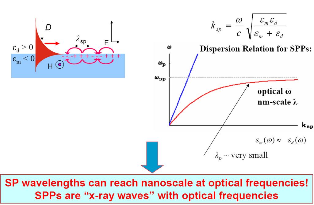
64 Applications in Technology Plasmons have been considered as a means of transmitting information on computer chips, since plasmons can support much higher frequencies (into the 100 THz range, while conventional wires can not tolerate even tens of GHz. They have also been proposed as a means of high resolution lithography and microscopy due to their extremely small wavelengths. Both of these applications have seen successful demonstrations in laboratory environment.
65 Applications in Technology It is evident that deeply sub-wavelength focal spots cannot be formed through conventional focusing using a lens system or microscope objective. This is due, primarily, to the lack of high-index media at visible frequencies. What if, however, one was able to achieve a high effective index with conventional optical materials? That is the potential of surface plasmon optics. By employing geometries of conductors (such as metals or doped semiconductors) with dielectrics (such as air or glass), modes at optical frequencies can be created with effective indices of refraction that are orders of magnitude higher than those of the constituent materials. In fact, these indices can be so high as to create X-ray wavelengths (less than 10nm) with visible frequencies. The reason surface plasmon modes can achieve anomalously high wave-vectors at visible frequencies is because they are mediated by electrons rather than free space optical fields.
66 High Index of refraction Super Lenses?? EnergyDens ity 2eV (10 m) 19 J J / m 3 Energy of 2eV stored in a volume of 1nm 3 EnergyDens ity T 4 / c 0.2J / m 3 Energy density of our solar system
67 Applications in Technology The ability to focus the optical field to deeply subwavelength dimensions opens the door to an entirely new class of photonic devices. If one could combine the imaging powers of X-ray wavelengths with the economy and maturity of visible light sources, one could greatly broaden the practical engineering toolbox. Imagine focusing visible photons to spatial dimensions less than ten nanometers. By doing so, electron beam microscopy is immediately displaced by optical microscopy, replacing expensive electron beam sources with inexpensive visible lasers. Beyond simple economics, though, this achievement would allow for the nanoscale imaging of living biological samples.
68 Applications in Technology Combining Plasmonics Effects and Photonic Crystals Photonic band structure refers to the modification of the propagation properties of electromagnetic waves traveling through a periodically modulated dielectric. The effects of scattering and interference of the light by the periodic structure would result in a change in the propagation of the waves. The alteration in the propagation properties is particularly significant when the wavelength of the light is approximately equal to the spacing between the dielectric structures. In this regime photonic band gaps--frequency intervals in which no photon modes are allowed--can be created for appropriately designed dielectric arrays. The ability to create volumes of space in which no photons of a given band of energies can exist has a number of fundamental and applied consequences.
69 Application in Health Science Surface plasmon resonance is used by biochemists to detect the presence of a molecule on a surface. SPR reflectivity measurements can be used to detect DNA or proteins by the changes in the local index of refraction upon adsorption of the target molecule to the metal surface. If the surface is patterned with different biopolymers, the technique is denoted as Surface Plasmon Resonance Imaging (SPRI). For nanoparticles, localized surface plasmon oscillations can give rise to the intense colors of solutions of plasmon resonance nanoparticles and/or very intense scattering. Nanoparticles of noble metals exhibit strong ultraviolet-visible absorption bands that are not present in the bulk metal. Shifts in this resonance due to changes in the local index of refraction upon adsorption of biopolymers to the nanoparticles can be used to detect biopolymers such as DNA or proteins.
70 Application in Health Science Areas of interest in this domain are for instance the examination of protein-protein or protein-dna interactions, in order to detect conformation changes in an immobilized protein. In addition to above mentioned, biosensors may also be used to monitor the glucose levels in diabetic patients. The system under study would be based upon direct measurements of the reflection and transmission spectra in the near infrared spectrum.
71 Application in Health Science Drug discovery Traditionally drugs were discovered via tedious efforts, however with the advent of biosensors this process may be sped up. Biosensors offer the possibility of detecting the interaction between a particular target and a possible drug. This is made possible without the use of markers or the detection of color changes of fluorescence, which in turn eliminates any potential cause of interference and furthermore test samples do not need to be purified and can be reused. Biosensors also have the capability of measuring how quickly and how well a potential drug binds to a target.

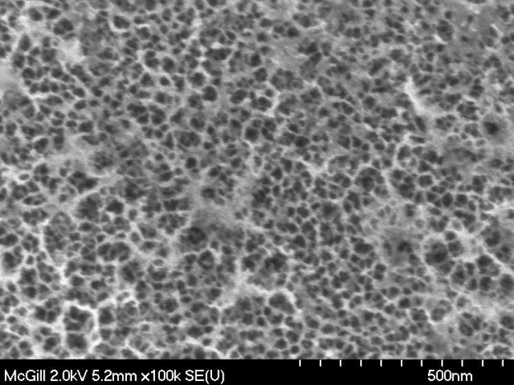
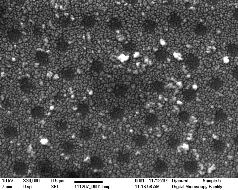
72 Researches done in our group AFM of Au-PS colloidal crystal (Au can t be seen here too small) Ordered multilayers of composites layers PS microspheres: 510 nm; Au: 5 nm Vertical deposition 55 o C, 3 days 72


 a) V d = 100")
73 Self-Assembly Techniques S. Badilescu, M. Kahrizi, Journal of Materials Science: Materials, 2007 nanospheres colloidal crystal Aluminium cap Meniscus back Meniscus front Surface dropping velocity PS Au suspension topcock Substrate z Inclination angle x Water evaporation Attractive capillary forces Meniscus region Convective flow (a) a) V d = 100 µm/s b) Vd = 40 µm/s c) Vd = 15 µm/s (b) (c)


74 Results Sample prepared with 200 nm PS Spheres not annealed Nanohole present evenly distributed Sample prepared with 200 nm PS Spheres not annealed Nanoholes present some imperfections 74

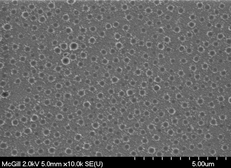
75 Nanocups Nanorings Nanoholes fabricated using Porous Silicon Method
76

77
78 Potential Applications Optical Biosensor Mirror Nanoholes metallic structure Cladding Core A.R. Hajiaboli & M. Kahrizi,.. CSTC, 2007

79 An Example to fabricate periodic nanostructures Fabricated many samples PS sphere sizes: 100 nm, 200 nm, 500 nm and 700 nm Resulted in hole and ring structures Ring structures are not continuous ring structures - made of nanoparticles which do not touch one another Some samples were annealed and some were not Observed aggregation effects around holes for certain samples Observed PS spheres not completely removed in some cases Sample prepared with 700 nm PS Spheres not annealed Nanorings and nanoholes present Aggregation effects around holes Size of holes is less than the size of spheres 79

80 Nanohole/nanoring array prepared with 530 nm PS and 20 nm Au more rings Sample annealed at 90 0 C for 20 min Inset: enlarged image of a region where PS spheres were not completely removed. - Au nanoparticles are around and on the top of the spheres
81 Sample Preparation Silanization Amino Silane will bond to Au Silane Molecule NH 2 R Si Amino Group Organic Radical Substrate OH group on substrate will react with silane molecule 81

 added to boiled solution Solution")

82 Sample Preparation Preparation of Colloidal Au by Reduction of Chloroauric Acid mg of chloroauric acid is dissolved in ~80mL of DI water solution heated Solution begins to boil - Au sodium citrate solution (1%) added to boiled solution Solution boiled for another minutes - left to cool down to room temperature Once ready the solution became a deep red/purple 82

83 Sample Preparation Sample Preparation: Self-Assembly Silanized Substrate Silanized sample immersed in Au and PS mixture Multilayer of Au and PS composite structure formed by self assembly Substrate kept in this mixture at C For 2-3 days 83

84 Results Structure of the Au Nanoparticles X-ray diffraction patterns of PS-Au composite Trace a and b depict presence of Au, Trace c refers to sample with very low amount of Au Trace a weak peaks= less Au, Trace b stronger peak = more Au Trace b indicates 6-9 nm particle sizes Gold Crystalline Structure - fcc 84
85 Results Geometrical Characteristics Average spacing of the holes increases linearly with diameter of PS spheres Average hole diameter increases linearly with diameter of PS spheres Density of the holes decreases as sphere sizes increases Sensitivity decreases as spacing increases between holes Sensitivity increases for smaller spheres 85
86 Results UV-VIS Spectrum of a Nanohole/Nanoring Array - Sensitivity of the Structure (/n) A) In water and B) 2-PROPANOL (sample annealed for 30 min at 110C) Au LSPR band red-shifted by 8 nm in 2-propanol S = 340 nm/riu 86
87 Sample Preparation Expression of Protein (AT5G0701.1) and Production of Antibody Preparation was done in collaboration with the Department of Biology at Concordia University Adsorption of Antibody on the sensor platform: Dilution Incubation of Polyclonal antibody 1 hour Rinsing of the platform Recording of spectrum Adsorption of Protein on the sensor platform: Incubation of AT5G Adsorption of BSA Rinsing of the platform Recording of spectrum 87
88 Sample Preparation Functionalization and Adsorption of Protein and Antibody Glass Au nanoparticle film functionalized with 3-mercaptopropionic acid Adsorption of Protein and Antibody Glass 88
89 Spectra corresponding to the protein-antibody interaction: A) spectrum of the functionalized substrate using Au that was prepared in the lab B) spectrum of the antibody adsorbed on the substrate C) spectrum of the previously absorbed antibody followed by the adsorption of the protein on the substrate Observed shift of +10 nm when antibody adsorbed After protein adsorption no additional shift but observed shoulder around 600 nm 89
90 Results Biomolecular Interactions cont d Sandwiched system: Using the previous system additional antibody layer adsorbed Spectrum corresponding to the protein sandwiched between two antibody layers: A) Spectrum of the functionalized substrate with antibody and protein adsorption using Au that was prepared in the lab B) spectrum when an additional antibody layer is adsorbed on the system corresponding to trace A Additional antibody layer results in shift of +10 nm 90
 42-amino acid")
91 Results Biomolecular Interactions Interaction with Amyloid β Derived Diffusible Ligands (ADDL) ADDL is a biological molecule that may cause neurological dysfunctions relevant to memory associated to Alzheimer s disease Alzheimer s disease leading cause of dementia in people over age of 65 First patient diagnosed with Alzheimer s disease was in 1906 Aguste D Amyloid beta (Aβ) 42-amino acid peptide involved in neurotoxic assemblies Amyloid plaques causes: Neuronal degeneration Memory loss Progressive dementia (Aβ) protein monomers present in humans not toxic until assemble into amyloid fibrils ADDLs are 3-24mers of (Aβ) monomer and are potent Affect central nervous system Memory loss Elevated levels of ADDLs in autopsied brains of Alzheimer s disease subjects 91
92 Sample Preparation Preparation of ADDL Preparation was done in collaboration with the Department of Biology at Concordia University Prepared by the Lambert Protocol Two parts to the procedure: PART I: Monomerization (polymer that defragments into monomers) by HFIP and storage of Aβ peptide PART II: Preparation of ADDL 92
93 Results Biomolecular Interactions cont d ADDL deposited on functionalized gold structures Left in contact with sensor platform for 24 hours Large shift of LSPR band observed Δλ = 30nm Δλ = λ in PBS without ADDL λ in PBS with ADDL 93
94 Results Raman Characteristics Detection of Marine toxins using Au nanostructures: Gonyautoxin/Saxitoxin-e GTX II: R1, R3 and R4= H, R2 = OSO3 GTX III: R1, R2 and R4= H, R3 = OSO3 Very toxic and an analytical method, without complicated preparation, is very important. The samples are simply drop-coated on the gold nanostructure, dried and then, measured. Structures of both toxins similar position of radicals different 94
 B On DCDR substrate Experimental condition Filter : No filter C 250 500")
95 Biomedical Sensors (SPR devices) On 5 nm Au network Experimental condition Filter : D1 (reduces the incident radion by 10 times) Spectrophotometry Intensity (counts/sec) ,2 1,0 0,8 0,6 0,4 0, A On DCDR substrate Experimental condition Filter : D1 (reduces the incident radion by 10 times) B On DCDR substrate Experimental condition Filter : No filter C Wavenumber (cm -1 ) A. R. Hajiabol & M.Kahrizi, CSTC 2007 Comparing the Raman intensity to the toxin on DCDR substrate (commercially available)
Nanophotonics: principle and application. Khai Q. Le Lecture 11 Optical biosensors
 Nanophotonics: principle and application Khai Q. Le Lecture 11 Optical biosensors Outline Biosensors: Introduction Optical Biosensors Label-Free Biosensor: Ringresonator Theory Measurements: Bulk sensing
Plasmonics: Application-oriented fabrication. Part 1. Introduction
 Plasmonics: Application-oriented fabrication Part 1. Introduction Victor Ovchinnikov Department of Aalto Nanofab Aalto University Espoo, Finland Alvar Aalto was a famous Finnish architect and designer
Basics of Plasmonics
 Basics of Plasmonics Min Qiu Laboratory of Photonics and Microwave Engineering School of Information and Communication Technology Royal Institute of Technology (KTH) Electrum 229, 16440 Kista, Sweden http://www.nanophotonics.se/
Engineering in the Optimization of Resolution of Nanohole Arrays in Metal Films for Refractive Index Sensing
 Engineering in the Optimization of Resolution of Nanohole Arrays in Metal Films for Refractive Index Sensing by Gabriela Andrea Cervantes Téllez B.Sc., Instituto Tecnológico de Estudios Superiores de Monterrey,
CREOL, The College of Optics & Photonics, University of Central Florida
 Metal Substrate Induced Control of Ag Nanoparticle Plasmon Resonances for Tunable SERS Substrates Pieter G. Kik 1, Amitabh Ghoshal 1, Manuel Marquez 2 and Min Hu 1 1 CREOL, The College of Optics and Photonics,
Biomarker Discovery using Surface Plasmon Resonance Imaging
 F e a t u r e A r t i c l e Feature Article Biomarker Discovery using Surface Plasmon Resonance Imaging Elodie LY-MORIN, Sophie BELLON, Géraldine MÉLIZZI, Chiraz FRYDMAN Surface Plasmon Resonance (SPR)
Plasmonic Nanostructures II
 Plasmonic Nanostructures II Dr. Krüger / Prof. M. Zacharias, IMTEK, Propagation of SPPs Propagation distance decreases with decreasing strip width! 2 Dr. Krüger / Prof. M. Zacharias, IMTEK, Bound and leaky
Solar Cells and Photosensors.
 Designing Photonic Crystals in Strongly Absorbing Material for Applications in Solar Cells and Photosensors. Minda Wagenmaker 1, Ebuka S. Arinze 2, Botong Qiu 2, Susanna M. Thon 2 1 Mechanical Engineering
Experiment 2b X-Ray Diffraction* Optical Diffraction Experiments
 * Experiment 2b X-Ray Diffraction* Adapted from Teaching General Chemistry: A Materials Science Companion by A. B. Ellis et al.: ACS, Washington, DC (1993). Introduction Inorganic chemists, physicists,
Satoshi Kawata. Near-Field Optic s and Surface Plasmon Polaritons
 Satoshi Kawata Near-Field Optic s and Surface Plasmon Polaritons Near-Field Optics and the Surface Plasmon Polariton Dieter W. Pohl 1 1. Introduction 1 2. Back to the Roots 1 2.1. Rayleigh and Mie Scattering
Silver Diffusion Bonding and Layer Transfer of Lithium Niobate to Silicon
 Chapter 5 Silver Diffusion Bonding and Layer Transfer of Lithium Niobate to Silicon 5.1 Introduction In this chapter, we discuss a method of metallic bonding between two deposited silver layers. A diffusion
ADOPT Winter School Merging silicon photonics and plasmonics
 ADOPT Winter School 2014 Merging silicon photonics and plasmonics Prof. Min Qiu Optics and Photonics, Royal Institute of Technology, Sweden and Optical Engineering, Zhejiang University, China Contents
OMICS Group signed an agreement with more than International Societies to make healthcare informati on Open Access. OMICS Group Conferences
 About Omics Group OMICS Group International through its Open Ac cess Initiative is committed to make genuine an d reliable contributions to the scientific commu nity. OMICS Group hosts over 400 leading-edg
Light Trapping Enhancement in Thin Film Silicon Solar Cell with Different Back Reflector
 International Journal of Electrical Components and Energy Conversion 2017; 3(5): 83-87 http://www.sciencepublishinggroup.com/j/ijecec doi: 10.11648/j.ijecec.20170305.11 ISSN: 2469-8040 (Print); ISSN: 2469-8059
Phil Saunders, spacechannel.org
 Guidi with Phil Saunders, spacechannel.org ng Light Long-Range nge Plasmons Aloyse Degiron, Pierre Berini and David R. Smith Long-range surface plasmons are optical modes propagating along metallic circuits
Interferometric optical biosensor. Xingwei Wang
 Interferometric optical biosensor Xingwei Wang 1 Light Transverse electromagnetic wave Reflection Refraction Diffraction Interference 2 Fabry-Perot interferometer 3 Interferometer Two waves that coincide
Analysis of strongly absorbing chromophores by UV-visible ATR spectroscopy
 Technical Note: AN 915 Rev. B Analysis of strongly absorbing chromophores by UV-visible ATR spectroscopy Walter M. Doyle and Lani Tran This paper illustrates the potential of the attenuated total reflectance
Coatings. Ion Assisted Deposition (IAD) process Advance Plasma Source (APS) plasma-ion assisted Deposition. Coatings on Optical Fibers
 process Advance Plasma Source (APS) plasma-ion assisted Deposition. Coatings on Optical Fibers") Anti-Reflection Custom Ion Assisted Deposition (IAD) process Advance Plasma Source (APS) plasma-ion assisted Deposition Anti-Reflection on Optical Fibers OptoSigma supplies a wide selection of optical
Anti-Reflection Custom Ion Assisted Deposition (IAD) process Advance Plasma Source (APS) plasma-ion assisted Deposition Anti-Reflection on Optical Fibers OptoSigma supplies a wide selection of optical
High Resolution X-ray Diffraction
 High Resolution X-ray Diffraction Nina Heinig with data from Dr. Zhihao Donovan Chen, Panalytical and slides from Colorado State University Outline Watlab s new tool: Panalytical MRD system Techniques:
Optical Control of Surface Plasmon Coupling in Organic Light Emitting Devices with Nanosized Multi-cathode Structure
 Proceedings of the 5 th International Conference on Nanotechnology: Fundamentals and Applications Prague, Czech Republic, August 11-13, 2014 Paper No. 234 Optical Control of Coupling in Organic Light Emitting
Digital resolution enhancement in surface plasmon microscopy
 Digital resolution enhancement in surface plasmon microscopy I.I. Smolyaninov 1) *, J. Elliott 2), G. Wurtz 2), A.V. Zayats 2), C.C. Davis 1) 1) Department of Electrical and Computer Engineering, University
Trench Structure Improvement of Thermo-Optic Waveguides
 International Journal of Applied Science and Engineering 2007. 5, 1: 1-5 Trench Structure Improvement of Thermo-Optic Waveguides Fang-Lin Chao * Chaoyang University of Technology, Wufong, Taichung County
average diameter = 3 nm, from PlasmaChem) was mixed in NLCs to produce QDembedded
 was mixed in NLCs to produce QDembedded") Electronic Supplementary Material (ESI) for RSC Advances. This journal is The Royal Society of Chemistry 2014 Supporting information Experimental Section The blended CLC-monomer materials used to fabricate
Electronic Supplementary Material (ESI) for RSC Advances. This journal is The Royal Society of Chemistry 2014 Supporting information Experimental Section The blended CLC-monomer materials used to fabricate
Photonic Drying Pulsed Light as a low Temperature Sintering Process
 Photonic Drying Pulsed Light as a low Temperature Sintering Process Lou Panico Xenon Corporation W E S T E R N M I C H I G A N U N I V E R S I T Y PRESENTATION OVERVIEW What is Printed Electronics Materials
Challenges and Future Directions of Laser Fuse Processing in Memory Repair
 Challenges and Future Directions of Laser Fuse Processing in Memory Repair Bo Gu, * T. Coughlin, B. Maxwell, J. Griffiths, J. Lee, J. Cordingley, S. Johnson, E. Karagiannis, J. Ehrmann GSI Lumonics, Inc.
LPR Sensor Made by Using Ordered Porous Alumina
 UDC 669.716.9+669.218+534.428+615.076 LPR Sensor Made by Using Ordered Porous Alumina Yuichi TOMARU*, Takeharu TANI*, Yoshinori HOTTA**, Yusuke HATANAKA**, and Masayuki NAYA* Abstract We fabricated a LPR
9/28/2013 9:26 PM. Chapter 3. The structure of crystalline solids. Dr. Mohammad Abuhaiba, PE
 Chapter 3 The structure of crystalline solids 1 2 Why study the structure of crystalline solids? Properties of some materials are directly related to their crystal structure. Significant property differences
Modification of Glass by FS Laser for Optical/Memory Applications
 Modification of Glass by FS Laser for Optical/Memory Applications Kazuyuki Hirao and Kiyotaka Miura Department of Material Chemistry Kyoto University International Workshop on Scientific Challenges of
9/16/ :30 PM. Chapter 3. The structure of crystalline solids. Mohammad Suliman Abuhaiba, Ph.D., PE
 Chapter 3 The structure of crystalline solids 1 Mohammad Suliman Abuhaiba, Ph.D., PE 2 Home Work Assignments HW 1 2, 7, 12, 17, 22, 29, 34, 39, 44, 48, 53, 58, 63 Due Sunday 17/9/2015 3 Why study the structure
Optical Coatings. Photonics 4 Luxury Coatings , Genève. Dr. Andreas Bächli Head of Optical Coatings at RhySearch, Buchs (SG)
") Optical Coatings Photonics 4 Luxury Coatings 21.06.2017, Genève Dr. Andreas Bächli Head of Optical Coatings at RhySearch, Buchs (SG) RhySearch The Research- and Innovation Center in the Rhine Valley RhySearch
Optical Coatings Photonics 4 Luxury Coatings 21.06.2017, Genève Dr. Andreas Bächli Head of Optical Coatings at RhySearch, Buchs (SG) RhySearch The Research- and Innovation Center in the Rhine Valley RhySearch
Fs- Using Ultrafast Lasers to Add New Functionality to Glass
 An IMI Video Reproduction of Invited Lectures from the 17th University Glass Conference Fs- Using Ultrafast Lasers to Add New Functionality to Glass Denise M. Krol University of California, Davis 17th
Understanding Optical Coatings For Military Applications
 Understanding Optical Coatings For Military Applications By Trey Turner, Chief Technology Officer, REO Virtually all optical components used in military applications, such as target designation, rangefinding
Advances in Intense Pulsed Light Solutions For Display Manufacturing. XENON Corporation Dr. Saad Ahmed Japan IDW 2016
 Advances in Intense Pulsed Light Solutions For Display Manufacturing XENON Corporation Dr. Saad Ahmed Japan IDW 2016 Talk Outline Introduction to Pulsed Light Applications in Display UV Curing Applications
Time-resolved Measurements Using the Agilent Cary Eclipse Fluorescence Spectrophotometer A Versatile Instrument for Accurate Measurements
 Time-resolved Measurements Using the Agilent Cary Eclipse Fluorescence Spectrophotometer A Versatile Instrument for Accurate Measurements Technical Overview Authors Dr. Fabian Zieschang, Katherine MacNamara,
4 Concept of Ripple Pyrometry during Flash Lamp Annealing
 4 Concept of Ripple Pyrometry during Flash Lamp Annealing 4.1 Review on Temperature Measurement for Flash Lamp Annealing Several different efforts have been undertaken to measure temperature by contactless
Simulating Plasmon Effect in Nanostructured OLED Cathode Using COMSOL Multiphysics
 Simulating Plasmon Effect in Nanostructured OLED Cathode Using COMSOL Multiphysics Leiming Wang *, Jun Amano, and Po-Chieh Hung Konica Minolta Laboratory USA Inc. *Corresponding author: 2855 Campus Drive
Structure and optical properties of M/ZnO (M=Au, Cu, Pt) nanocomposites
 nanocomposites") Solar Energy Materials & Solar Cells 8 () 339 38 Structure and optical properties of M/ (M=Au, Cu, Pt) nanocomposites U. Pal a,b, *, J. Garc!ıa-Serrano a, G. Casarrubias-Segura a, N. Koshizaki c, T. Sasaki
Solar Energy Materials & Solar Cells 8 () 339 38 Structure and optical properties of M/ (M=Au, Cu, Pt) nanocomposites U. Pal a,b, *, J. Garc!ıa-Serrano a, G. Casarrubias-Segura a, N. Koshizaki c, T. Sasaki
Scintillating Optical Fibers
 Scintillating Optical Fibers Plastic Scintillating Fibers Saint-Gobain Crystals manufactures a variety of plastic scintillating, wavelength-shifting and light-transmitting fibers used for research and
Qswitched lasers are gaining more interest because of their ability for various applications in remote sensing, environmental monitoring, micro
 90 Qswitched lasers are gaining more interest because of their ability for various applications in remote sensing, environmental monitoring, micro machining, nonlinear frequency generation, laserinduced
Chemistry 145 Exam number 4 name 11/19/98 # Faraday s constant is 96,500 c/mole of electrons.
 Chemistry 145 Exam number 4 name 11/19/98 # Faraday s constant is 96,500 c/mole of electrons. A.(16) An electrochemical cell is prepared with a strip of manganese metal dipping in to a 1.0 M MnSO 4 solution
Characterization of laser-material interaction during laser cladding process P.-A. Vetter,* J. Fontaine,* T. Engel," L. Lagrange,& T.
 Characterization of laser-material interaction during laser cladding process P.-A. Vetter,* J. Fontaine,* T. Engel," L. Lagrange,& T. Marchione^ f^, BID de /a rzcfozre ^7000 France ABSTRACT The interaction
Supplementary Figure 1 Scanning electron micrograph (SEM) of a groove-structured silicon substrate. The micropillars are ca. 10 μm wide, 20 μm high
 of a groove-structured silicon substrate. The micropillars are ca. 10 μm wide, 20 μm high") Supplementary Figure 1 Scanning electron micrograph (SEM) of a groove-structured silicon substrate. The micropillars are ca. 10 μm wide, 20 μm high and own the gap of 10 μm. Supplementary Figure 2 Strictly
Supplementary Figure 1 Scanning electron micrograph (SEM) of a groove-structured silicon substrate. The micropillars are ca. 10 μm wide, 20 μm high and own the gap of 10 μm. Supplementary Figure 2 Strictly
Solvent Correction versus In-line Reference Measurement
 Technical Note Solvent Correction versus In-line Reference Measurement Optical systems such as SPR and BLI often have difficulty with nonspecific noise when measuring low molecular weight analyte in organic
Specimen Preparation Technique for a Microstructure Analysis Using the Focused Ion Beam Process
 Specimen Preparation Technique for a Microstructure Analysis Using the Focused Ion Beam Process by Kozue Yabusaki * and Hirokazu Sasaki * In recent years the FIB technique has been widely used for specimen
Label-free interaction analysis in realtime using surface plasmon resonance
 GE Healthcare Technology Note 23 Biacore systems Label-free interaction analysis in realtime using surface plasmon resonance Providing quantitative data on: report point Specificity sensorgram To what
Cellular imaging using Nano- Materials. A Case-Study based approach Arun Murali, Srivats V
 Cellular imaging using Nano- Materials A Case-Study based approach Arun Murali, Srivats V Agenda Discuss a few papers Explain a couple of new imaging techniques and their benefits over conventional imaging
Transmission Electron Microscopy (TEM) Prof.Dr.Figen KAYA
 Prof.Dr.Figen KAYA") Transmission Electron Microscopy (TEM) Prof.Dr.Figen KAYA Transmission Electron Microscope A transmission electron microscope, similar to a transmission light microscope, has the following components along
Transmission Electron Microscopy (TEM) Prof.Dr.Figen KAYA Transmission Electron Microscope A transmission electron microscope, similar to a transmission light microscope, has the following components along
What is Hydrologic Optics? Optics Attentuation Inherent properties Scatter Absorption Apparent properties
 1 of 7 3/22/2006 1:29 PM Water quality research Water quality Hydrologic optics Components of water quality SERC water research projects CISNet program What is Hydrologic Optics? Optics Attentuation Inherent
7-2E. Photonic crystals
 7-2E. Photonic crystals Purdue Univ, Prof. Shalaev, http://cobweb.ecn.purdue.edu/~shalaev/ Univ Central Florida, CREOL, Prof Kik, http://sharepoint.optics.ucf.edu/kik/ose6938i/handouts/forms/allitems.aspx
Carbon nanostructures. (http://www.mf.mpg.de/de/abteilungen/schuetz/index.php?lang=en&content=researchtopics&type=specific&name=h2storage)
") Carbon nanostructures (http://www.mf.mpg.de/de/abteilungen/schuetz/index.php?lang=en&content=researchtopics&type=specific&name=h2storage) 1 Crystal Structures Crystalline Material: atoms arrange into a
Carbon nanostructures (http://www.mf.mpg.de/de/abteilungen/schuetz/index.php?lang=en&content=researchtopics&type=specific&name=h2storage) 1 Crystal Structures Crystalline Material: atoms arrange into a
VACUUM VIEWPORTS. Introduction... I 03 KF Viewports... I 09 I 01. VACUUM / Components & Consumables
 I VAUUM VIEWPORTS Introduction... I 03 KF Viewports... I 09 I I 01 Neyco manufactures a range of UHV viewports in F, ISO or KF flange styles including a variety of coatings to enhance performance. Materials
Growth Of TiO 2 Films By RF Magnetron Sputtering Studies On The Structural And Optical Properties
 Journal of Multidisciplinary Engineering Science and Technology (JMEST) Growth Of TiO 2 Films By RF Magnetron Sputtering Studies On The Structural And Optical Properties Ahmed K. Abbas 1, Mohammed K. Khalaf
Introduction of Biosensors
 Introduction of Biosensors Lecture April 17 Jeff T.H.Wang website: http://pegasus.me.jhu.edu/~thwang/ New course : BioMEMS and BioSensing (Spring 04 ) What s is a biosensor? Target 4.22 Signal Signal Analtye
Oxide Growth. 1. Introduction
 Oxide Growth 1. Introduction Development of high-quality silicon dioxide (SiO2) has helped to establish the dominance of silicon in the production of commercial integrated circuits. Among all the various
Measurement of Residual Stress by X-ray Diffraction
 Measurement of Residual Stress by X-ray Diffraction C-563 Overview Definitions Origin Methods of determination of residual stresses Method of X-ray diffraction (details) References End Stress and Strain
Photovoltaics under concentrated sunlight
 Photovoltaics under concentrated sunlight April 2, 2013 The University of Toledo, Department of Physics and Astronomy Principles and Varieties of Solar Energy (PHYS 4400) Reading assignment: Sections 9.4
LOW TEMPERATURE PHOTONIC SINTERING FOR PRINTED ELECTRONICS. Dr. Saad Ahmed XENON Corporation November 19, 2015
 LOW TEMPERATURE PHOTONIC SINTERING FOR PRINTED ELECTRONICS Dr. Saad Ahmed XENON Corporation November 19, 2015 Topics Introduction to Pulsed Light Photonic sintering for Printed Electronics R&D Tools for
Fluorescence Microscopy. Terms and concepts to know: 10/11/2011. Visible spectrum (of light) and energy
 and energy") Fluorescence Microscopy Louisiana Tech University Ruston, Louisiana Microscopy Workshop Dr. Mark DeCoster Associate Professor Biomedical Engineering 1 Terms and concepts to know: Signal to Noise Excitation
Fluorescence Microscopy Louisiana Tech University Ruston, Louisiana Microscopy Workshop Dr. Mark DeCoster Associate Professor Biomedical Engineering 1 Terms and concepts to know: Signal to Noise Excitation
Lecture 22: Integrated circuit fabrication
 Lecture 22: Integrated circuit fabrication Contents 1 Introduction 1 2 Layering 4 3 Patterning 7 4 Doping 8 4.1 Thermal diffusion......................... 10 4.2 Ion implantation.........................
Metallization deposition and etching. Material mainly taken from Campbell, UCCS
 Metallization deposition and etching Material mainly taken from Campbell, UCCS Application Metallization is back-end processing Metals used are aluminum and copper Mainly involves deposition and etching,
Laser Micromachining of Bulk Substrates and Thin Films Celine Bansal
 Laser Micromachining of Bulk Substrates and Thin Films Celine Bansal Oxford Lasers Ltd Moorbrook Park Didcot, Oxfordshire, OX11 7HP Tel: +44 (0) 1235 810088 www.oxfordlasers.com Outline Oxford Lasers Importance
Study on Infrared Absorption Characteristics of Ti and TiN x Nanofilms. Mingquan Yuan, Xiaoxiong Zhou, Xiaomei Yu
 10.119/1.36982 The Electrochemical Society Study on Infrared Absorption Characteristics of Ti and TiN x Nanofilms Mingquan Yuan, Xiaoxiong Zhou, Xiaomei Yu National Key Laboratory of Science and Technology
MI USA. 1, Eggenstein-Leopoldshafen, Germany. Engineering, University of Michigan, Ann Arbor, MI USA
 Evaluating UV/H 2 O 2 Exposure as a DEHP Degradation Treatment for Plasticized PVC Jeanne M. Hankett 1, Alexander Welle 2,3, Joerg Lahann 4, Zhan Chen 1 * 1 Department of Chemistry, University of Michigan,
Electron microscopy II
 Electron microscopy II Nanomaterials characterization I RNDr. Věra Vodičková, PhD. Interaction ction: electrons solid matter Signal types SE.secondary e - AE Auger s e - BSE back scattered e - X-ray photons,
High Transmittance Ti doped ITO Transparent Conducting Layer Applying to UV-LED. Y. H. Lin and C. Y. Liu
 High Transmittance Ti doped ITO Transparent Conducting Layer Applying to UV-LED Y. H. Lin and C. Y. Liu Department of Chemical Engineering and Materials Engineering, National Central University, Jhongli,
High-energy x-ray production with pyroelectric crystals
 JOURNAL OF APPLIED PHYSICS 97, 104916 2005 High-energy x-ray production with pyroelectric crystals Jeffrey A. Geuther a and Yaron Danon Department of Mechanical, Aerospace, and Nuclear Engineering, Rensselaer
Polymer-based optical interconnects using nano-imprint lithography
 Polymer-based optical interconnects using nano-imprint lithography Arjen Boersma,Sjoukje Wiegersma Bert Jan Offrein, Jeroen Duis, Jos Delis, Markus Ortsiefer, Geert van Steenberge, MikkoKarppinen, Alfons
POLYMER STABILIZED CHOLESTERIC DICHROIC DYE DISPLAYS
 POLYMER STABILIZED CHOLESTERIC DICHROIC DYE DISPLAYS Fang Zhang, Julie Kim, Mary Neubert and Deng-Ke Yang Chemical Physics Program and Liquid Crystal Institute Kent State University, Kent, OH 22 Abstract
BIOSENOSRS BIO 580. Nanobiosensors WEEK-13 Fall Semester. Faculty: Dr. Javed H. Niazi KM Faculty of Engineering & Natural Sciences Sabanci University
 BIOSENOSRS BIO 580 Nanobiosensors WEEK-13 Fall Semester Faculty: Dr. Javed H. Niazi KM Faculty of Engineering & Natural Sciences Sabanci University Topics that will be covered in the course History of
In-Situ Monitoring of Pattern Filling in Nano-Imprint Lithography Using Surface Plasmon Resonance
 Copyright 2011 American Scientific Publishers All rights reserved Printed in the United States of America Journal of Nanoscience and Nanotechnology Vol. 11, 1 6, 2011 In-Situ Monitoring of Pattern Filling
NanoSystemsEngineering: NanoNose Final Status, March 2011
 1 NanoSystemsEngineering: NanoNose Final Status, March 2011 The Nanonose project is based on four research projects (VCSELs, 3D nanolithography, coatings and system integration). Below, the major achievements
Application Note #124 VITA: Quantitative Nanoscale Characterization and Unambiguous Material Identification for Polymers
 Local thermal analysis identifies polymer AFM image of polymer blend Application Note #124 VITA: Quantitative Nanoscale Characterization and Unambiguous Material Identification for Polymers VITA module
Efficient, broadband and compact metal grating couplers for silicon-on-insulator waveguides
 Efficient, broadband and compact metal grating couplers for silicon-on-insulator waveguides Stijn Scheerlinck, Jonathan Schrauwen, Frederik Van Laere, Dirk Taillaert, Dries Van Thourhout and Roel Baets
Design Optimization of Structural Parameters for Highly Sensitive Photonic Crystal Label-Free Biosensors
 Sensors 2013, 13, 3232-3241; doi:10.3390/s130303232 Article OPEN ACCESS sensors ISSN 1424-8220 www.mdpi.com/journal/sensors Design Optimization of Structural Parameters for Highly Sensitive Photonic Crystal
A LIDAR SYSTEM FOR REMOTE MEASUREMENT OF OIL FILM THICKNESS ON SEA SURFACE *
 A LIDAR SYSTEM FOR REMOTE MEASUREMENT OF OIL FILM THICKNESS ON SEA SURFACE * Jacek Piskozub, Violetta Drozdowska Institute of Oceanology PAS, Sopot, Poland; email: piskozub@iopan.gda Viktor Varlamov Institute
High Power Operation of Cryogenic Yb:YAG. K. F. Wall, B. Pati, and P. F. Moulton Photonics West 2007 San Jose, CA January 23, 2007
 High Power Operation of Cryogenic Yb:YAG K. F. Wall, B. Pati, and P. F. Moulton Photonics West 2007 San Jose, CA January 23, 2007 Outline Early work on cryogenic lasers MPS laser technology Recent program
The Raman effect, discovered in 1928 by C.V. Raman in his
 Refined Raman Spectroscopy Bringing New Insight into INDUSTRIAL PROCESSES Sophie Morel and Fran Adar Fiber probes and ease of use make Raman spectroscopy systems attractive for monitoring process control
Periodic Metallic Nanostructures as Plasmonic Chemical Sensors
 pubs.acs.org/langmuir Periodic Metallic Nanostructures as Plasmonic Chemical Sensors Chiara Valsecchi and Alexandre G. Brolo* Department of Chemistry, University of Victoria, P.O. Box 3065, Victoria, BC,
BIO 315 Lab Exam I. Section #: Name:
 Section #: Name: Also provide this information on the computer grid sheet given to you. (Section # in special code box) BIO 315 Lab Exam I 1. In labeling the parts of a standard compound light microscope
Optical Coatings. Phone: Fax: Domostroitelnaya str St. Petersburg, Russia
 The Fresnel reflection at the boundary of media with different refractive indices and interference in thin films allow the optical components reflecting and transmitting properties to be selectively and
Damage Threats and Response of Final Optics for Laser-Fusion Power Plants
 Damage Threats and Response of Final Optics for Laser-Fusion Power Plants M. S. Tillack 1, S. A. Payne 2, N. M. Ghoniem 3, M. R. Zaghloul 1 and J. F. Latkowski 2 1 UC San Diego, La Jolla, CA 92093-0417
Supporting Information for Manuscript B516757D
 Supporting Information for Manuscript B516757D 1. UV-Vis absorption spectra Absorbance (a.u.) 0.4 0.2 5F 6F 7F 0.0 300 400 500 Wavelength (nm) Figure S1 UV-Vis spectra of, 5F, 6F and 7F in CHCl 3 solutions
X-ray Photoelectron Spectroscopy
 X-ray Photoelectron Spectroscopy X-ray photoelectron spectroscopy (XPS) is a non-destructive technique used to analyze the elemental compositions, chemical and electronic states of materials. XPS has a
Basics of Solar Photovoltaics. Photovoltaics (PV) Lecture-21
 Lecture-21") Lecture-21 Basics of Solar Photovoltaics Photovoltaics (PV) Photovoltaics (PV) comprise the technology to convert sunlight directly into electricity. The term photo means light and voltaic, electricity.
Lecture-21 Basics of Solar Photovoltaics Photovoltaics (PV) Photovoltaics (PV) comprise the technology to convert sunlight directly into electricity. The term photo means light and voltaic, electricity.
Semiconductor Technology
 Semiconductor Technology from A to Z Oxidation www.halbleiter.org Contents Contents List of Figures List of Tables II III 1 Oxidation 1 1.1 Overview..................................... 1 1.1.1 Application...............................
Plastic Coated Silica/Silica (Low OH) FIBER CROSS SECTION Polyimide and Acrylate Coated. Nylon and Tefzel Coated
 FIBER CROSS SECTION Polyimide and Acrylate Coated. Nylon and Tefzel Coated") DESCRIPTION When looking for a high quality fiber with superior transmission and a numerical aperture (N.A.) of 0.22 for efficient light coupling, the is the fiber of choice. The Anhydroguide fiber is
DESCRIPTION When looking for a high quality fiber with superior transmission and a numerical aperture (N.A.) of 0.22 for efficient light coupling, the is the fiber of choice. The Anhydroguide fiber is
Quiz on Monday covering: -symmetry operations -notations of axes, vectors, and face notation -Miller indices
 OTHER ANNOUNCEMENTS Quiz on Monday covering: -symmetry operations -notations of axes, vectors, and face notation -Miller indices 2 nd Draft of References due Monday Field Trip Saturday 10/4 and Sunday
Photonic Sintering of Silver for Roll-to-Roll Printed Electronics. Saad Ahmed, PhD Manager-Engineering
 Photonic Sintering of Silver for Roll-to-Roll Printed Electronics Saad Ahmed, PhD Manager-Engineering Topics Introduction Significance of nanotechnology Conductive inks Pulsed light for sintering Reel-to-reel
Shape Light Beams. Using Plasmonics to. Federico Capasso, Nanfang Yu, Ertugrul Cubukcu and Elizabeth Smythe
 Using Plasmonics to Shape Light Beams Federico Capasso, Nanfang Yu, Ertugrul Cubukcu and Elizabeth Smythe Plasmonic structures shape semiconductor laser beams. Left: A plasmonic collimator spreads out
X-Ray Diffraction by Macromolecules
 N. Kasai M. Kakudo X-Ray Diffraction by Macromolecules With 351 Figures and 56 Tables Kodansha ~Springer ... Contents Preface v Part I Fundamental 1. Essential Properties of X-Rays................. 3 1.1
Measuring Manganese Concentration Using Spectrophotometry
 Measuring Manganese Concentration Using Spectrophotometry Objectives To use spectroscopy to determine the amount of Manganese is an unknown sample. Scenario Your have just joined a "Green Team" at the
Instrument Configuration for Powder Diffraction
 Instrument Configuration for Powder Diffraction Advanced X-ray Workshop S.N. Bose National Centre for Basic Sciences, 14-15/12/2011 Innovation with Integrity Overview What is the application? What are
PULSED LASER WELDING
 PULSED LASER WELDING Girish P. Kelkar, Ph.D. Girish Kelkar, Ph.D, WJM Technologies, Cerritos, CA 90703, USA Laser welding is finding growing acceptance in field of manufacturing as price of lasers have
University of Michigan
 University of Michigan Department of Mechanical Engineering Low-cost Non-invasive Diagnosis of Malaria Infected Red Blood Cells Han Yu Undergraduate Student Department of Electrical Engineering and Computer
350 C for 8 hours in argon atmosphere. Supplementary Figures. Supplementary Figure 1 High-temperature annealing of BP flakes on SiO 2.
 Supplementary Figures Supplementary Figure 1 High-temperature annealing of BP flakes on SiO 2. (a-d) The optical images of three BP flakes on a SiO 2 substrate before (a,b) and after annealing (c,d) at
Glass Processing Course
 Glass Processing Course Lecture 4. COLOR IN COMMERCIAL GLASSES JAMES E. SHELBY Professor Emeritus Alfred University shelbyje@alfred.edu Spring 2015 An Online-learning resource from the IMI-NFG Lecture
Characterization of Materials with a Combined AFM/Raman Microscope
 Characterization of Materials with a Combined AFM/Raman Microscope Marko Surtchev 1, Sergei Magonov 1 and Mark Wall 2 1 NT-MDT America, Tempe, AZ U.S.A. 2 Thermo Fisher Scientific, Madison, WI, U.S.A.
Fabrication and Layout
 ECEN454 Digital Integrated Circuit Design Fabrication and Layout ECEN 454 3.1 A Glimpse at MOS Device Polysilicon Aluminum ECEN 475 4.2 1 Material Classification Insulators Glass, diamond, silicon oxide
Precision Optical Engineering
 Precision Optical Engineering Products: Prisms Windows Mirrors Flats and Master angles Sight Glasses Key Features: Prisms (Contacted, Cemented, AR coated, Mounted) Windows (Flat, wedged, curved, drilled,
Supplementary Material (ESI) for Chemical Communications This journal is (c) The Royal Society of Chemistry 2009
 for Chemical Communications This journal is (c) The Royal Society of Chemistry 2009") Supplementary Information Silver Nanoparticles with Planar Twinned Defects: Effect of Halides for Precise Tuning of Plasmon Absorption from 400 to >900 nm by Nicole Cathcart, Andrew J. Frank and Vladimir
Supplementary Information Silver Nanoparticles with Planar Twinned Defects: Effect of Halides for Precise Tuning of Plasmon Absorption from 400 to >900 nm by Nicole Cathcart, Andrew J. Frank and Vladimir