Mode conversion in two-dimensional magneto-photonic crystal waveguide made by fully compatible optical sol-gel matrix
|
|
|
- Jewel Burke
- 6 years ago
- Views:
Transcription
1 Optica Applicata, Vol. XLVI, No. 4, 216 DOI: /oa1645 Mode conversion in two-dimensional magneto-photonic crystal waveguide made by fully compatible optical sol-gel matrix AHMED KAHLOUCHE *, ABDESSELAM HOCINI, DJAMEL KHEDROUCHE Laboratoire d Analyse des Signaux et Systèmes (LASS), Département d Electronique, Faculté de Technologie, Université Mohamed Boudiaf de M sila, BP.166, Route Ichebilia, M sila 28, Algeria * Corresponding author: kahlouche_ahmed@yahoo.fr In this paper, we have reported a theoretical study of the mode conversion in two-dimensional magneto-photonic crystal waveguide. The structure is formed by a triangular lattice of air holes embedded in a composite matrix SiO 2 /ZrO 2 or SiO 2 /TiO 2. These new magneto-optical materials are developed by organic-inorganic sol-gel process and doped with ferrite of cobalt nanoparticles (CoFe 2 O 4 ). The modal birefringence and conversion output have been calculated by varying, respectively, the film thickness and the magnetic nanoparticles concentration. The obtained results show an enhancement in the TE-TM mode conversion. Thus, when the amount of cobalt ferrite nanoparticles reaches 39% into sol-gel matrix, the efficiency can reach 95% which proves that such structures have very promising potential for creating integrated optical isolators. Keywords: magneto-photonic crystal waveguides, modal birefringence, optical isolator, mode conversion TE-TM. 1. Introduction Magneto-optical isolators are the essential nonreciprocal devices which are used in optical communication systems. These components are based on the Faraday rotation effect of magneto-optical materials and its nonreciprocal behavior [1, 2]. Optical isolators allow the transmission of light in only one direction and block it in the opposite direction. Because of this performance, the optical isolator is necessary for protecting other optical active devices such as an amplifier and laser source from unwanted reflections [3, 4]. Nowadays, there is a strong interest in the miniaturization of nonreciprocal devices in order to integrate all optical components on a unique substrate. Several years ago, the material widely used to fabricate bulk optical isolators is the ferrimagnetic garnet oxide crystal yttrium iron garnet (YIG), or bismuth substituted yttrium iron garnet (Bi:YIG) deposited on a gadolinium gallium garnet (GGG) substrate [5]. However, this class of

![which is as high as 7 C [6]. In the other hand, the use of GGG as a substrate is not commonly used to realize integrated functions based on III-V semiconductor, silica, silicon and polymer [7].](/docs-images/75/72968751/images/2-1.jpg "To overcome these problems, several groups of research have developed a novel approach based on a composite magneto-optical matrix doped with magnetic nanoparticles [8, 9].")
2 566 A. KAHLOUCHE et al. material cannot be easily embedded by classical technologies to realize magneto-optical integrated devices because the annealing temperature needed for the crystallization of magnetic Iron Garnet which is as high as 7 C [6]. In the other hand, the use of GGG as a substrate is not commonly used to realize integrated functions based on III-V semiconductor, silica, silicon and polymer [7]. To overcome these problems, several groups of research have developed a novel approach based on a composite magneto-optical matrix doped with magnetic nanoparticles [8, 9]. Sol-gel process can be used to prepare a large variety of thin films obtained on several substrates (glass, silicon) and fully compatible with planar magneto-photonic crystal waveguides [1, 11]. The magneto-optical materials made by SiO 2 /ZrO 2 or SiO 2 /TiO 2 matrix doped with 1.5% of cobalt ferrite (CoFe 2 O 4 ) present an interest Faraday rotation about 32 deg/cm at 1.55 μm, but it is suffering from a low merit factor, which is the quality ratio between the Faraday rotation and the absorption (F = θ F /α [deg cm 1 /cm 1 ]), it is about 12 deg at 1.55 μm for planar waveguides [12]. However, this value of a merit factor is motivating, but is not enough to consider this magneto-optical material as a good candidate for integrated applications. Based on our previous paper [13], we present in this paper a new structure called 2D magneto-photonic crystal waveguides which are used for amplifying the magneto -optical effects in order to enhance the merit factor. Using a beam propagation method (BPM) [14], we look to investigate the influence of the volume fraction of magnetic nanoparticles and the film thickness on the mode conversion in 2D magneto-photonic waveguides formed with a triangular lattice of circular air holes. 2. Two-dimensional photonic crystal The two-dimensional photonic crystal to be studied and analyzed in this work is shown in Fig. 1a. The structure consists of a triangular lattice of circular air holes embedded in a SiO 2 /ZrO 2 or SiO 2 /TiO 2 organic-inorganic matrix. The air holes have a radius of.36a, where a is the lattice constant (a = 75 nm). However, the triangular lattice al- Air hole a SiO 2 /TiO 2 matrix 54 nm 75 nm Frequency (ωa/2πc = a/λ) b TE TM Γ M K Γ Fig. 1. The 2D photonic crystal structure formed by a triangular lattice of air holes in a composite matrix (a), and TE/TM band structure for a 2D photonic crystal formed by a triangular lattice of circular air holes in a composite matrix SiO 2 /TiO 2 (b).
3 Mode conversion in 2D magneto-photonic crystal waveguide T a b l e 1. Refractive index of the host matrix at 1.55 μm [17]. Ratio SiO 2 /ZrO 2 or TiO 2 Precursors Index at 1.55 μm Sol 1/3 SiO 2, ZrO Sol 1/7 SiO 2, ZrO Sol 1/1 SiO 2, ZrO Sol 1/12 SiO 2, TiO Sol 1/1 SiO 2, TiO lows the opening of 2D photonic band gap, presents a good compromise, namely for high felling factors, and it is lowly sensitive to the incidence angle compared to the square lattice [15, 16]. Moreover, the triangular lattice is expected to serve a good platform for photonic integrated circuits. The composite matrix is prepared by sol-gel process and is characterized by a weak and a flexible index which can be changed in the range 1.51 to 1.58 at the wavelength of telecommunications λ =1.55μm, as mentioned in Table 1 [17]. The 2D photonic crystal is characterized by a low refractive index (n = 1.58) [17]. Different results (obtained by using a 2D plane wave expansion (PWE) method) present simultaneously the photonic band gaps formed for both polarizations: transverse magnetic (TM) and transverse electric (TE). Figure 1b sketches the dispersions curves and band gaps which are calculated along the Γ M K Γ edge for the Brillouin zone of the structure without any defects, for both polarizations (TM and TE). On the one hand, we see that the largest band gap opened is for the TM polarization which is indicated by the hashed red region, it extends from normalized frequency a /λ =.468 to.55 whose corresponding wavelength ranges from λ =1.485μm to 1.62 μm. On the other hand, a narrow band gap will appear for the TE polarization, it extends from a /λ =.447 to.461 whose corresponding wavelength spans from λ =1.626μm to μm. Figures 2a and 2b show respectively the influence of a slab index on the size and position of the photonic band gaps for 2D photonic crystal described above. From Gap width (a/λ) a b r/a =.36 r/a = Gap center (a/λ) Slab index Slab index Fig. 2. Variation of the TM photonic band gap width (a), and variation of the wavelength center of TM photonic band gap (b) as a function of slab index for r/a =.36.
4 568 A. KAHLOUCHE et al. Gap width (a/λ) a a =.75 μm n = 1.58 Frequency (ωa/2πc) b n = Radius [μm] Radius [μm] Fig. 3. Band gap width as a function of air hole radius of a 2D photonic crystals (a). Gap map of 2D photonic crystals structure formed by a triangular lattice of circular air holes insert in sol-gel SiO 2 /TiO 2 matrix (b). results, we can conclude that the width of photonic band gaps is strongly influenced by the refractive index. The band width in normalized frequency was increased from Δ(a /λ) =.2547 for low index (n =1.51) to Δ(a /λ) =.3153 for high index (n = 1.58). On the other hand, the results demonstrate clearly that when the refractive index increases, the photonic band gap shifts towards the higher wavelengths, and the center wavelength λ c =(λ min + λ max )/2 varied from λ c = 1.51 μm to μm. In Figure 3a, we have reported the variations of the bandwidth as a function of air hole radius for a lattice period a =.75μm and a refractive index equal to The results show that the band gaps were opened from r =.131μm and vanished for a radius upper than.32 μm, and between the two boundaries of the radius, the size of a photonic band gap was varying like a Gaussian function with a hole radius. On the other hand, the bandwidth is maximum for r =.27μm, it was about 117 nm. Figure 3b depicts the gap map of the previous triangular structure for the TM polarization. We can observe that the forbidden band extends between a /λ =.4 and.56 when the radius of air holes is varied from.131 to.32 μm. Furthermore, the results show that the largest band gap was found around telecommunications wavelength λ =1.55μm, which corresponds to the TM polarization and it extends from λ min = μm to λ max =1.62μm. These results have been obtained by using the 2D PWE technique [14]. 3. Two-dimensional magneto-photonic waveguide Figure 4 shows the top view of the physical design that we analyze and simulate in K this work. It is a linear and symmetric 2D magneto-photonic waveguide ( W3 A ), which is realized on the wafer of SiO 2 /TiO 2 matrix by removing three rows of air holes in the Γ K direction. This kind of structure is called air-bridge structure which is surrounded by air (substrate and cover). The simulations are based on the known finite difference BPM of RSoft CAD [14]. This computational method is the most widely

5 Mode conversion in 2D magneto-photonic crystal waveguide x Air hole y H z z W Direction of propagation (ΓK) SiO 2 /TiO 2 matrix Fig. 4. Top view of a W3 waveguide in a 2D triangular lattice of air holes formed by removing three rows of holes along the Γ K direction. used propagation technique for modeling photonic devices and photonic integrated circuits. In this section, we will simulate the propagation in the waveguide by a Gaussian pulse excited from the light source with a normalized frequency centered at ω =.484(2c/a) with a frequency width of Δω =.4(2c/a) (c is the velocity of light in free space). The 2D photonic crystals are realized on a magneto-optical matrix of silica/titania (SiO 2 /TiO 2 ) doped with different volume fractions of cobalt ferrite nanoparticles and subjected to a magnetic field parallel to the direction of propagation. 4. Theory of the mode conversion Magneto-optical waveguides are the basic elements for nonreciprocal integrated optics. However, the application of a magnetic field on a magneto-optical material with a direction parallel to the light beam propagation (Oz) produces off-diagonal elements in a dielectric tensor where the magnitude depends on the Faraday rotation θ F and ellipticity ε F [18]. Faraday rotation depends on several parameters such as the nanoparticle size [19], the particle volume fraction [2], the applied magnetic field [21] and the light wavelength [22]. Similar to the Faraday rotation effect observed in free space, a nonreciprocal effect can be achieved in a planar waveguide by the TE-TM mode conversion under a longitudinal magnetic field, and TE-TM mode coupling of a guide is obtained. In the case of such structure, the magneto-optical permittivity tensor [ε ] is expressed in a Cartesian coordinate system {x, y, z} by: [ ε ] = ε 1 iε xy iε xy ε 1 ε 1 (1) where ε 1 and λ are respectively the value of diagonal elements of a permittivity tensor (ε 1 = ) and the wavelength of work.
6 57 A. KAHLOUCHE et al. The off-diagonal element (ε xy ) of a permittivity tensor leads to a coupling between the TE and TM modes. It strongly depends on the Faraday rotation θ F which is proportional to the concentration of magnetic nanoparticles Φ %, vacuum wavelength λ and the refractive index of the magneto-optical (mo) material ( n = ε 1 ). The magnitude of ε xy is given by the approximate relationship [23, 24]: θ F λ ε 1 ε xy = Im( ε mo ) = (2) π Here, for simplicity, we will ignore the absorption and assume ε 1 and ε xy to be real. If the incident mode is the transverse magnetic (TM), the conversion output R(z) is defined like the intensity ratio of the mode TE at the distance z on the intensity of the mode TM at the beginning (z = ) [5]: Rz ( ) = I TE( z) / I TM It can then be written as: ( ) (3) Rz ( ) = θ F sin 2 2 θ 2 θ F + ( Δβ /2) 2 F + ( Δβ /2) 2 z (4) From Eq. (4), it is clear that TE-TM mode conversion is strongly affected by the specific Faraday rotation θ F (deg/cm) of the material forming the waveguide and by the phase mismatch between TE and TM modes Δβ (deg/cm) which is given by Δβ = β TE β TM = ( N TE N TM ) π λ In practice, the difference between the TE and TM refractive index needs to be as low as possible for an efficient mode conversion. This later is obtained for a distance called the coupling length. When the difference of the phase Δβ is not zero, the conversion efficiency of the mode is limited to the value R M which is obtained at the end of a length of coupling L C, and it is given by the relationship [25]: L C = π θ F + ( Δβ ) 2 The maximum rate of mode conversion induced by a Faraday rotation effect can be expressed as: (5) (6) 2 θ F R M = θ F + ( Δβ /2) 2 (7)

, there is no coupling between TE and TM modes.")
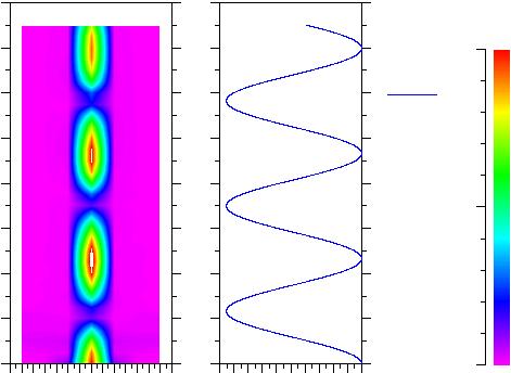
7 Mode conversion in 2D magneto-photonic crystal waveguide The effect of volume fraction on the mode conversion The analysis performed in this work has been concentrated on the TM polarization, for which the 2D photonic crystal exhibits a band gap between λ =1485nm and 162 nm. In Figure 5a, we report the E-field distribution inside the guide and the power flow through the waveguide for the TM mode. It is clear that, for an isotropic planar waveguide and hence for a zero magnetization (ε xy = ), there is no coupling between TE and TM modes. On the contrary, once the volume fraction of cobalt ferrite increases inside 2D magneto-photonic waveguide, so the magnitude of ε xy increases, and the modes start to couple between them. Figure 5b shows the E-field distribution and the mode conversion obtained with a BPM in the case of a sol-gel SiO 2 /TiO 2 matrix of thickness h =2.4μm and doped with 18% of CoFe 2 O 4 nanoparticles. The magnitude 6 1. a X [μm] Monitor value [a. u.] 6 1. b R M 6 L C X [μm] Monitor value [a. u.]. Fig. 5. Mode conversion in isotropic planar waveguide (a), mode conversion in 2D magneto-photonic waveguide doped with 18% of CoFe 2 O 4 nanoparticles (b).
8 572 A. KAHLOUCHE et al. Efficiency of mode conversion a h = 2.4 μm Magnitude of off-diagonal terms ε xy Coupling length [μm] h = 2.4 μm Magnitude of off-diagonal terms ε xy b Fig. 6. The influence of the off-diagonal elements ε xy for a sol-gel silica/titania matrix of thickness h =2.4μm: on the conversion output R M (a), and on the coupling length L C (b). of magneto-optical term ε xy is calculated using the corresponding value of θ F, derived from [25], and Eq. (2), and it is found to be Figures 6a and 6b report, respectively, the influence of the off-diagonal term ε xy on the conversion output R M and the coupling length L C for a slab of thickness h =2.4μm. We observe that, if the value of the off-diagonal term ε xy increases, the coupling length L C decreases and the maximal conversion R M increases, thus the time necessary to obtain the coupling decreases. Thus, the efficiency of mode conversion R M when the magneto-optical layer is doped with a weak concentration of magnetic nanoparticles ε xy =.16 is 52% and reached 95% for high concentration ε xy =.14. The coupling length is about 558 μm for ε xy =.16 and decreases to 115 μm for ε xy = The effect of slab height on the conversion output In the following section, we consider the magneto-photonic structure described above and doped with a high volume fraction of cobalt ferrite (39%) [25]. The Faraday rotation is about 834 deg/cm, consequently, the off-diagonal term of a permittivity tensor has the value ε xy =.14, which corresponds to a strong coupling between the TE/TM modes. Now, the light propagation inside the planar magneto-photonic waveguide is simulated as a function of various slab thickness to obtain the maximum mode conversion. The 3D BPM was employed in order to obtain different results which are depicted in Fig. 7. Figure 7 represents the variation of the conversion output and the coupling length according to the thickness of slab height h, for this concentration. It is observed that the conversion output increases proportionally to the increase in slab thickness h when the thickness of SiO 2 /TiO 2 film increases between 1.6 and 2.6 μm. The value of con-

![u.]. 6 6 1..5. X [μm] Monitor value [a. u.]. 8 1.](/docs-images/75/72968751/images/9-1.jpg "c 8 1. d 6 6 4 4 2 2 6 6 1..5. X [μm] Monitor value [a.")
![e 8 1. f 6 6 4 4 2 2 6 6 1..5. X [μm] Monitor value [a.](/docs-images/75/72968751/images/9-2.jpg "u.]. 6 6 1..5. X [μm] Monitor value [a. u.]. Fig. 7.")

, h =1.8μm (b), h =2.")
9 Mode conversion in 2D magneto-photonic crystal waveguide a 8 1. b X [μm] Monitor value [a. u.] X [μm] Monitor value [a. u.] c 8 1. d X [μm] Monitor value [a. u.] X [μm] Monitor value [a. u.] e 8 1. f X [μm] Monitor value [a. u.] X [μm] Monitor value [a. u.]. Fig. 7. The effect of thickness on the mode conversion in a 2D magneto-photonic waveguide structure formed by a triangular lattice of air holes in SiO 2 /TiO 2 matrix doped with 39% for: h =1.6μm (a), h =1.8μm (b), h =2.μm (c), h =2.2μm (d), h =2.4μm (e), and h =2.6μm (f ).
10 574 A. KAHLOUCHE et al. Efficiency of mode conversion ε xy = Thickness [μm] a Modal birefringence ΔN ε xy = Thickness [μm] b Fig. 8. The influence of the film thickness h on the mode conversion output (a) and on the phase mismatch (b) for a sol-gel matrix doped with 39% of CoFe 2 O 4. version output is 27.9% for h =1.6μm and it reaches the value of 95.34% for h =2.6μm. Beyond the value of 2.6 μm, the output conversion decreases and reaches 74.1% for h =4.μm as it is shown in Fig. 8a. 7. The effect of slab height on the modal birefringence The conception of a magneto-optical isolator that has an interesting nonreciprocal effect needs the maximization of R M. To achieve this goal, the amplitude of the specific Faraday rotation θ F (deg/cm) must be as high as possible, while the phase mismatch between TE and TM modes Δβ (deg/cm) must be as low as possible. This later is directly linked to the geometrical modal birefringence ΔN m for the mode number m by the following relationship [26]: 2π Δβ m = ΔN m λ (8) As it is shown in Fig. 8b, we have calculated the influence of the film thickness h on the modal birefringence (ΔN, m = ) for the mode TM. The obtained results show clearly that, if the slab thickness h increases, the modal birefringence decreases. Thus, for a sol-gel SiO 2 /TiO 2 matrix of thickness h =4.μm the modal birefringence between the fundamental TE and TM modes was equal to ΔN = , and it reaches for a slab thickness h =2.6μm. 8. Conclusion This paper describes a theoretical study of a 2D magneto-photonic waveguide formed by a triangular lattice of circular air holes embedded into silica/titania matrix. It is prepared via a sol-gel process and doped with ferrite of cobalt nanoparticles. This new magneto-optical material is fully compatible with classical substrates. Firstly, using
11 Mode conversion in 2D magneto-photonic crystal waveguide a 2D PWE method we have studied and analyzed the band diagrams and the gap maps in 2D photonic crystals in order to determine the photonic band gaps. Afterwards, an analysis of the mode conversion in a 2D magneto-photonic crystal waveguide has been presented, using the BPM, in order to provide a theoretical prediction of physical and geometrical parameters that lead to an efficient mode conversion and the enhancement of Faraday rotation. The obtained results show that the volume fraction of magnetic nanoparticles and the thickness of the film have a great influence on the mode conversion output and coupling length. We also found, for such structure, that the conversion output reaches 95% and the coupling length is lowered to 115 μm when the magnetic nanoparticles concentration increases to 39%. Finally, the calculation of the modal birefringence between the fundamental TE and TM modes, as a function of slab thickness, show clearly that a decrease in the modal birefringence occurs when the slab thickness is decreased. Consequently, the conversion output is strongly affected by the film thickness. A future work consists in studying the influence of the absorption coefficient on the TE/TM mode conversion in 2D magneto-photonic crystal waveguides devices. References [1] BAHLMANN N., LOHMEYER M., ZHUROMSKYY Q., DÖTSCH H., HERTEL P., Nonreciprocal coupled waveguides for integrated optical isolators and circulators for TM-modes, Optics Communications 161(4 6), 1999, pp [2] BAHLMANN N., LOHMEYER M., DÖTSCH H., HERTEL P., Integrated magneto-optic Mach Zehnder interferometer isolator for TE modes, Electronics Letters 34(22), 1998, pp [3] XIAOYUN GUO, ZAMAN T., RAM R.J., Magneto-optical semiconductor waveguides for integrated isolators, Proceedings of SPIE 5729, 25, pp [4] LANO G.E., PINYAN C., Optical isolators direct light the right way: fiberoptic components handbook, Laser Focus World 31(7), 1995, pp [5] LOHMEYER M., BAHLMANN N., ZHUROMSKYY O., DÖTSCH H., HERTEL P., Phase-matched rectangular magnetooptic waveguides for applications in integrated optics isolators: numerical assessment, Optics Communications 158(1 6), 1998, pp [6] HUANG M., XU Z.-C., Wavelength and temperature characteristics of BiYbIG film/yig crystal composite structure for magneto-optical applications, Applied Physics A 81(1), 25, pp [7] HUTCHINGS D.C., Prospects for the implementation of magneto-optic elements in optoelectronic integrated circuits: a personal perspective, Journal of Physics D: Applied Physics 36(18), 23, pp [8] HOCINI A., BOUMAZA T., BOUCHEMAT M., ROYER F., JAMON D., ROSSEAU J.J., Birefringence in magneto -optical rib waveguides made by SiO 2 /TiO 2 doped with γ -Fe 2 O 4, Microelectronics Journal 39(1), 28, pp [9] ROYER F., JAMON D., BROQUIN J.-E., AMATA H., KEKESI R., NEVEU S., BLANC-MIGNON M.-F., GHIBAUDO E., Fully compatible magneto-optical sol-gel material with glass waveguides technologies: application to mode converters, Proceedings of SPIE 7941, 211, article [1] SHOJI Y., MIZUMOTO T., YOKOI H., HSIEH I.-W., OSGOOD R.M., JR, Magneto-optical isolator with silicon waveguides fabricated by direct bonding, Applied Physics Letters 92(7), 28, article [11] JOUDRIER A.-L., COUCHAUD M., MORICEAU H., BROQUIN J.-E., FERRAND B., DESCHANVRES J.-L., Direct bonding conditions of ferrite garnet layer on ion-exchanged glass waveguides, Physica Status Solidi (A) 25(1), 28, pp
12 576 A. KAHLOUCHE et al. [12] CHOUEIKANI F., ROYER F., JAMON D., SIBLINI A., ROUSSEAU J.J., NEVEU S., CHARARA J., Magneto-optical waveguides made of cobalt ferrite nanoparticles embedded in silica/zirconia organic-inorganic matrix, Applied Physics Letters 94(5), 29, article [13] KAHLOUCHE A., HOCINI A., KHEDROUCHE D., Band-gap properties of 2D photonic crystal made by silica matrix doped with magnetic nanoparticles, Journal of Computational Electronics 13(2), 214, pp [14] Photonic Component Design Suite, BandSOLVE, BeamPROP from Rsoft Inc., [15] MATTHEWS A., WANG X.-H., KIVSHAR Y., GU M., Band-gap properties of two-dimensional low-index photonic crystals, Applied Physics B 81(2 3), 25, pp [16] DYOGTYEV A.V., SUKHOIVANOV I.A., DE LA RUE R.M., Photonic band-gap maps for different two dimensionally periodic photonic crystal structures, Journal of Applied Physics 17(1), 21, article [17] AMATA H., ROYER F., CHOUEIKANI F., JAMON D., BROQUIN J.-E., PLENET J.C., ROUSSEAU J.J., Magnetic nanoparticles-doped silica layer reported on ion-exchanged glass waveguide: towards integrated magneto-optical devices, Proceedings of SPIE 7719, 21, article 77191G. [18] WITTEKOEK S., POPMA T.J.A., ROBERTSON J.M., BONGERS P.F., Magneto-optic spectra and the dielectric tensor elements of bismuth substituted iron garnets at photon energies between ev, Physical Review B 12(7), 1975, p [19] ROYER F., JAMON D., ROUSSEAU J.J., CABUIL V., ZINS D., ROUX H., BOVIER C., Experimental investigation on γ -Fe 2 O 3 nanoparticles Faraday rotation: particles size dependence, European Physical Journal Applied Physics 22(2), 23, pp [2] KAHLOUCHE A., HOCINI A., KHEDROUCHE D., Mode conversion in 2D magneto photonic crystals made of SiO 2 /ZrO 2 matrix doped with magnetic nanoparticles, Acta Physica Polonica A 127(4), 215, pp [21] DAVIES H.W., LLEWELLYN J.P., Magneto-optic effects in ferrofluids, Journal of Physics D: Applied Physics 13(12), 198, pp [22] DONATINI F., JAMON D., MONIN J., NEVEU S., Experimental investigation of longitudinal magneto-optic effects in four ferrite ferrofluids in visible-near infrared spectrum, IEEE Transactions on Magnetics 35(5), 1999, pp [23] BOURAS M., HOCINI A., Mode conversion in magneto-optic rib waveguide made by silica matrix doped with magnetic nanoparticles, Optics Communications 363, 216, pp [24] HOCINI A., BOUMAZA T., BOUCHEMAT M., CHOUEIKANI F., ROYER F., ROUSSEAU J.J., Modeling and analysis of birefringence in magneto-optical thin film made by SiO 2 /ZrO 2 doped with ferrite of cobalt, Applied Physics B 99(3), 21, pp [25] KEKESI R., ROYER F., JAMONA D., BLANC-MIGNON M.F., ABOU-DIWAN E., CHATELON J.P., NEVEU S., TOMBACZ E., 3D magneto-photonic crystal made with cobalt ferrite nanoparticles silica composite structured as inverse opal, Optical Materials Express 3(7), 213, pp [26] HOCINI A., BOUCHELAGHEM A., SAIGAA D., BOURAS M., BOUMAZA T., BOUCHEMAT M., Birefringence properties of magneto-optic rib waveguide as a function of refractive index, Journal of Computational Electronics 12(1), 213, pp Received December 23, 215 in revised form March 15, 216
Monolithic Microphotonic Optical Isolator
 Monolithic Microphotonic Optical Isolator Lei Bi, Juejun Hu, Dong Hun Kim, Peng Jiang, Gerald F Dionne, Caroline A Ross, L.C. Kimerling Dept. of Materials Science and Engineering Massachusetts Institute
INTEGRATED OPTICAL ISOLATOR
 INTEGRATED OPTICAL ISOLATOR Presented by Gokhan Ozgur Advisor: Dr. Gary Evans July 02, 2004 Electrical Engineering - SMU INTRODUCTION They are used to eliminate light that is back-reflected, from splices
SUPPLEMENTARY INFORMATION
 SUPPLEMENTARY INFORMATION doi:.38/nphoton..7 Supplementary Information On-chip optical isolation in monolithically integrated nonreciprocal optical resonators Lei Bi *, Juejun Hu, Peng Jiang, Dong Hun
Trench Structure Improvement of Thermo-Optic Waveguides
 International Journal of Applied Science and Engineering 2007. 5, 1: 1-5 Trench Structure Improvement of Thermo-Optic Waveguides Fang-Lin Chao * Chaoyang University of Technology, Wufong, Taichung County
Modeling Of A Diffraction Grating Coupled Waveguide Based Biosensor For Microfluidic Applications Yixuan Wu* 1, Mark L. Adams 1 1
 Modeling Of A Diffraction Grating Coupled Waveguide Based Biosensor For Microfluidic Applications Yixuan Wu* 1, Mark L. Adams 1 1 Auburn University *yzw0040@auburn.edu Abstract: A diffraction grating coupled
7-2E. Photonic crystals
 7-2E. Photonic crystals Purdue Univ, Prof. Shalaev, http://cobweb.ecn.purdue.edu/~shalaev/ Univ Central Florida, CREOL, Prof Kik, http://sharepoint.optics.ucf.edu/kik/ose6938i/handouts/forms/allitems.aspx
Plasmonics using Metal Nanoparticles. Tammy K. Lee and Parama Pal ECE 580 Nano-Electro-Opto-Bio
 Plasmonics using Metal Nanoparticles Tammy K. Lee and Parama Pal ECE 580 Nano-Electro-Opto-Bio April 1, 2007 Motivation Why study plasmonics? Miniaturization of optics and photonics to subwavelength scales
Properties of Inverse Opal Photonic Crystals Grown By Atomic Layer Deposition
 Properties of Inverse Opal Photonic Crystals Grown By Atomic Layer Deposition J.S. King 1, C. W. Neff 1, W. Park 2, D. Morton 3, E. Forsythe 3, S. Blomquist 3, and C. J. Summers 1 (1) School of Materials
Rectangular Junction Ferrite Component in Millimeter Waves
 PIERS ONLINE, VOL. 4, NO. 5, 2008 526 Rectangular Junction Ferrite Component in Millimeter Waves D. Vincent Saint-Etienne University, France Abstract The design of non reciprocal components still remains
ATOMIC LAYER DEPOSITION FOR PHOTONIC CRYSTAL DEVICES
 ATOMIC LAYER DEPOSITION FOR PHOTONIC CRYSTAL DEVICES E. Graugnard, J. S. King, D. Heineman, and C. J. Summers School of Materials Science and Engineering, Georgia Institute of Technology, Atlanta, GA,
Electromagneto-Optical Scanning of the Magnetic Domains Local Areas of Bismuth-Substituted Yttrium Iron Garnets
 Journal of Modern Physics,,, 98-9 doi:.6/jmp..87 Published Online August (http://www.scirp.org/journal/jmp) Electromagneto-Optical Scanning of the Magnetic Domains Local Areas of Bismuth-Substituted Yttrium
Multilayer Silver / Dielectric Thin-Film Coated Hollow Waveguides for Sensor and Laser Power Delivery Applications
 Multilayer Silver / Dielectric Thin-Film Coated Hollow Waveguides for Sensor and Laser Power Delivery Applications Theory, Design, and Fabrication Carlos M. Bledt a, James A. Harrington a, and Jason M.
Nanostructured Engineered Materials With High Magneto-optic Performance For Integrated Photonics Applications
 Edith Cowan University Research Online School of Engineering Publications 28 Nanostructured Engineered Materials With High Magneto-optic Performance For Integrated Photonics Applications Mikhail Vasiliev
Characterisation of Fe-Ni amorphous thin films for possible magnetostrictive sensor applications
 Characterisation of Fe-Ni amorphous thin films for possible magnetostrictive sensor applications Contents 9.1 Introduction 9.2 Experiment 9.3 Results and Discussions 9.4 Conclusion 9.1 Introduction Magnetostrictive
PROJECT PERIODIC REPORT
 PROJECT PERIODIC REPORT Grant Agreement number: 619456 Project acronym: SITOGA Project title: Silicon CMOS compatible transition metal oxide technology for boosting highly integrated photonic devices with
THIN-FILM MAGNETLESS FARADAY ROTATORS FOR COMPACT HETEROGENEOUS INTEGRATED OPTICAL ISOLATORS
 THIN-FILM MAGNETLESS FARADAY ROTATORS FOR COMPACT HETEROGENEOUS INTEGRATED OPTICAL ISOLATORS Dolendra Karki 1, Vincent Stenger 2, Andrea Pollick 2, Miguel Levy 1 1 Physics Department, Michigan Technological
Study of the Band Gap of Photonic Crystal Fiber
 Study of the Band Gap of Photonic Crystal Fiber 1 LEBBAL MOHAMED REDHA, 2 SALIM GHALEM, 3 AHLEM BENMERKHI, 4 BOUCHEMAT TOURAYA, 5 BOUCHEMAT MOHAMED 1, 2, 3, 4, 5 Department of Electronics, Laboratory L.M.I.,
Seminar: Structural characterization of photonic crystals based on synthetic and natural opals. Olga Kavtreva. July 19, 2005
 Seminar: Structural characterization of photonic crystals based on synthetic and natural opals Olga Kavtreva July 19, 2005 Abstract Novel class of dielectric structures with a refractive index which exhibits
Ultrahigh Figure-of-Merit in Metal-Insulator-Metal Magnetoplasmonic Sensors Using Low Loss Magneto-optical Oxide Thin Films
 Supplementary Information Ultrahigh Figure-of-Merit in Metal-Insulator-Metal Magnetoplasmonic Sensors Using Low Loss Magneto-optical Oxide Thin Films Jun Qin,, Yan Zhang,, Xiao Liang,, Chuan Liu,, Chuangtang
Vertical plasmonic nanowires for 3D nanoparticle trapping
 Vertical plasmonic nanowires for 3D nanoparticle trapping Jingzhi Wu, Xiaosong Gan * Centre for Micro-Photonics, Faculty of Engineering and Industrial Sciences, Swinburne University of Technology, PO Box
Light Trapping Enhancement in Thin Film Silicon Solar Cell with Different Back Reflector
 International Journal of Electrical Components and Energy Conversion 2017; 3(5): 83-87 http://www.sciencepublishinggroup.com/j/ijecec doi: 10.11648/j.ijecec.20170305.11 ISSN: 2469-8040 (Print); ISSN: 2469-8059
Nanostructured engineered materials with high magneto-optic performance for integrated photonics applications
 Edith Cowan University Research Online ECU Presentations 2008 Nanostructured engineered materials with high magneto-optic performance for integrated photonics applications Mikhail Vasiliev Edith Cowan
Magnetic Field Sensors And Visualizers Using Magnetic Photonic Crystals
 Edith Cowan University Research Online ECU Publications Pre. Magnetic Field Sensors And Visualizers Using Magnetic Photonic Crystals Mikhail Vasiliev Edith Cowan University Kamal Alameh Edith Cowan University
1. Photonic crystal band-edge lasers
 TIGP Nanoscience A Part 1: Photonic Crystals 1. Photonic crystal band-edge lasers 2. Photonic crystal defect lasers 3. Electrically-pumped photonic crystal lasers 1. Photonic crystal band-edge lasers Min-Hsiung
Dielectric II-VI and IV-VI Metal Chalcogenide Thin Films in Hollow Glass Waveguides (HGWs) for Infrared Spectroscopy and Laser Delivery
 for Infrared Spectroscopy and Laser Delivery") Dielectric II-VI and IV-VI Metal Chalcogenide Thin Films in Hollow Glass Waveguides (HGWs) for Infrared Spectroscopy and Laser Delivery Carlos M. Bledt * a, Daniel V. Kopp a, and James A. Harrington a
Dielectric II-VI and IV-VI Metal Chalcogenide Thin Films in Hollow Glass Waveguides (HGWs) for Infrared Spectroscopy and Laser Delivery Carlos M. Bledt * a, Daniel V. Kopp a, and James A. Harrington a
Growth, Characterisation, And Properties of Bi1.8Lu1.2Fe3.6Al1.4O12 Garnet Films Prepared Using Two Different Substrate Temperatures
 Edith Cowan University Research Online ECU Publications Post 2013 2014 Growth, Characterisation, And Properties of Bi1.8Lu1.2Fe3.6Al1.4O12 Garnet Films Prepared Using Two Different Substrate Temperatures
Enhanced Light Trapping in Periodic Aluminum Nanorod Arrays as Cavity Resonator
 Enhanced Light Trapping in Periodic Aluminum Nanorod Arrays as Cavity Resonator Rosure B. Abdulrahman, Arif S. Alagoz, Tansel Karabacak Department of Applied Science, University of Arkansas at Little Rock,
Supplementary Information
 Electronic Supplementary Material (ESI) for Nanoscale. This journal is The Royal Society of Chemistry 2017 Supplementary Information Spatially Controlled Positioning of Coordination Polymer Nanoparticles
Amorphous silicon waveguides for microphotonics
 4 Amorphous silicon waveguides for microphotonics Amorphous silicon a-si was made by ion irradiation of crystalline silicon with 1 10 15 Xe ions cm 2 at 77 K in the 1 4 MeV energy range. Thermal relaxation
Potassium Titanyl Phosphate (KTP) Crystals
 Crystals") CASIX, Inc. Crystals Potassium Titanyl Phosphate (KTP) Crystals CASIX s KTP crystals feature high purity, low absorption at fundamental and second harmonic generation wavelengths. We supply super grade
CASIX, Inc. Crystals Potassium Titanyl Phosphate (KTP) Crystals CASIX s KTP crystals feature high purity, low absorption at fundamental and second harmonic generation wavelengths. We supply super grade
PATTERNING OF OXIDE THIN FILMS BY UV-LASER ABLATION
 Journal of Optoelectronics and Advanced Materials Vol. 7, No. 3, June 2005, p. 1191-1195 Invited lecture PATTERNING OF OXIDE THIN FILMS BY UV-LASER ABLATION J. Ihlemann * Laser-Laboratorium Göttingen e.v.,
Crystalline Silicon Solar Cells
 12 Crystalline Silicon Solar Cells As we already discussed in Chapter 6, most semiconductor materials have a crystalline lattice structure. As a starting point for our discussion on crystalline silicon
TEMPERATURE-DEPENDENT REFRACTIVE INDICES OF OPTICAL PLANAR WAVEGUIDES
 TEMPERATURE-DEPENDENT REFRACTIVE INDICES OF OPTICAL PLANAR WAVEGUIDES Aiman Kassir a, Abang Annuar Ehsan b, Noraspalelawati Razali b, Mohd Kamil Abd Rahman a and Sahbudin Shaari b Faculty of Applied Sciences,
ECE 541/ME 541 Microelectronic Fabrication Techniques
 ECE 541/ME 541 Microelectronic Fabrication Techniques MW 4:00-5:15 pm Metrology and Characterization Zheng Yang ERF 3017, email: yangzhen@uic.edu ECE541/ME541 Microelectronic Fabrication Techniques Page
Longitudinal Strain Sensitive Effect in a Photonic Crystal Cavity
 Longitudinal Strain Sensitive Effect in a Photonic Crystal Cavity Author Tung, Bui Thanh, Dao, Dzung Viet, Ikeda, Taro, Kanamori, Yoshiaki, Hane, Kazuhiro, Sugiyama, Susumu Published 2011 Conference Title
Solar Cells and Photosensors.
 Designing Photonic Crystals in Strongly Absorbing Material for Applications in Solar Cells and Photosensors. Minda Wagenmaker 1, Ebuka S. Arinze 2, Botong Qiu 2, Susanna M. Thon 2 1 Mechanical Engineering
Challenges and Future Directions of Laser Fuse Processing in Memory Repair
 Challenges and Future Directions of Laser Fuse Processing in Memory Repair Bo Gu, * T. Coughlin, B. Maxwell, J. Griffiths, J. Lee, J. Cordingley, S. Johnson, E. Karagiannis, J. Ehrmann GSI Lumonics, Inc.
Taimur Ahmed. Chalmers University of Technology, Sweden
 Taimur Ahmed Chalmers University of Technology, Sweden Background Ferromagnetics Ferroelectrics Multiferroics BiFeO 3 (BFO) Design & modeling of dielectric response Device fabrication Characterization
Fiber lasers. 1 Introduction. 2 Optical bers. Rui Miguel Cordeiro (F141104) April 13, 2015
 April 13, 2015") Fiber lasers Rui Miguel Cordeiro (F141104) April 13, 2015 1 Introduction Fiber lasers are, by denition, lasers in which the gain media is an optical ber. Sometimes, laser devices in which the output is
Fiber lasers Rui Miguel Cordeiro (F141104) April 13, 2015 1 Introduction Fiber lasers are, by denition, lasers in which the gain media is an optical ber. Sometimes, laser devices in which the output is
Ellipsometry as a tool for identifying process issues in roll-to-roll sputter deposited metal-oxide coatings
 Ellipsometry as a tool for identifying process issues in roll-to-roll sputter deposited metal-oxide coatings Sharon Louch Centre for Process Innovation, Wilton Centre, edcar. UK. TS10 3H Abstract Ellipsometry
Surface plasmon dielectric waveguides
 Surface plasmon dielectric waveguides Igor I. Smolyaninov, Yu-Ju Hung, and Christopher C. Davis Department of Electrical and Computer Engineering, University of Maryland, College Park, MD 20742 Phone:
Optical parameter determination of ZrO 2 thin films prepared by sol gel dip coating
 International Journal of ChemTech Research CODEN (USA): IJCRGG ISSN : 0974-490 Vol.6, No.13, pp 534-5346, November 014 MESCon 014 [4th -5 th September 014] National Conference on Material for Energy Storage
Neodymium doped GGG laser compared with YAP, SLGO and YAG lasers.
 Neodymium doped GGG laser compared with YAP, SLGO and YAG lasers. S.Kaczmarek 1, K.Kopczyński 1, T.Łukasiewicz 2, A.N. Durygin 3, I.M. Solskii 3 1-Institute of Optoelectronics, Military University of Technology,
Simple UV-based Soft-lithography Process for. Fabrication of Low-Loss Polymer PSQ-L-based. Waveguides
 Simple UV-based Soft-lithography Process for Fabrication of Low-Loss Polymer PSQ-L-based Waveguides Jie Teng 1, 2, 4, Stijn Scheerlinck 4, Geert Morthier 4, Roel Baets 4, Hongbo Zhang 2,3, Xigao Jian 2,3,
Wavelength and Temperature Dependence of the Er +3 Concentration in the Erbium Doped Fiber Amplifier
 Research Journal of Applied Sciences, Engineering and Technology 2(4): 396-400, 2010 ISSN: 2040-7467 Maxwell Scientific Organization, 2010 Submitted Date: May 09, 2010 Accepted Date: May 22, 2010 Published
FIBRE-COUPLED HIGH-INDEX PECVD SILICON- OXYNITRIDE WAVEGUIDES ON SILICON
 FIBRE-COUPLED HIGH-INDEX PECVD SILICON- OXYNITRIDE WAVEGUIDES ON SILICON Maxim Fadel and Edgar Voges University of Dortmund, High Frequency Institute, Friedrich-Woehler Weg 4, 44227 Dortmund, Germany ABSTRACT
CEMS study on diluted magneto titanium oxide films prepared by pulsed laser deposition
 Hyperfine Interact (2006) 168:1065 1071 DOI 10.1007/s10751-006-9406-2 CEMS study on diluted magneto titanium oxide films prepared by pulsed laser deposition K. Nomura & K. Inaba & S. Iio & T. Hitosugi
Passive TCF Compensation in High Q Silicon Micromechanical Resonators
 Passive TCF Compensation in High Q Silicon Micromechanical Resonators A.K. Samarao, G. Casinovi and F. Ayazi IEEE International Conference on Micro Electro Mechanical Systems pp. 116 119, January 2010
Enhanced and suppressed transmission through metal gratings at the plasmonic band edges
 Enhanced and suppressed transmission through metal gratings at the plasmonic band edges M. J. Bloemer, D. de Ceglia*, M. A. Vincenti*, M. Scalora, N. Akozbek Charles M. Bowden Laboratory, AMSRD-AMR-WS,
REAGENTLESS SENSORS WAVEGUIDE GRATING COUPLING SENSORS MACH-ZEHNDER INTERFEROMETER SENSORS SURFACE PLASMON RESONANCE SENSORS
 REAGENTLESS SENSORS WAVEGUIDE GRATING COUPLING SENSORS MACH-ZEHNDER INTERFEROMETER SENSORS SURFACE PLASMON RESONANCE SENSORS Reagentless Grating Coupler Sensor Angle, θ, is related to the analyte refractive
Synthesis and Characterization of Zinc Iron Sulphide (ZnFeS) Of Varying Zinc Ion Concentration
 Of Varying Zinc Ion Concentration") International Journal of Science and Technology Volume 5 No. 5, May, 2016 Synthesis and Characterization of Zinc Iron Sulphide (ZnFeS) Of Varying Zinc Ion Concentration I. B. Obasi 1 and J. C. Osuwa 2
International Journal of Science and Technology Volume 5 No. 5, May, 2016 Synthesis and Characterization of Zinc Iron Sulphide (ZnFeS) Of Varying Zinc Ion Concentration I. B. Obasi 1 and J. C. Osuwa 2
Nanorice Chain Waveguides Based on Low and High Order Mode Coupling
 Nanorice Chain Waveguides Based on Low and High Order Mode Coupling Xudong Cui, and Daniel Erni General and Theoretical Electrical Engineering (ATE), Faculty of Engineering, University of Duisburg- Essen,
High Performance Optical Coatings Deposited Using Closed Field Magnetron Sputtering
 High Performance Optical Coatings Deposited Using Closed Field Magnetron Sputtering D.R. Gibson, I.T. Brinkley, and J.L. Martin Applied Multilayers LLC, 1801 SE Commerce Avenue, Battle Ground, WA 98604
Vertical nano-composite heteroepitaxial thin films with manganites and ferroelectrics. Yonghang Pei Physics Department
 Vertical nano-composite heteroepitaxial thin films with manganites and ferroelectrics Yonghang Pei Physics Department Outline Introduction to MultiFerroics La 1 x Sr x MnO 3 Experiment Summary and Future
Design Optimization of Structural Parameters for Highly Sensitive Photonic Crystal Label-Free Biosensors
 Sensors 2013, 13, 3232-3241; doi:10.3390/s130303232 Article OPEN ACCESS sensors ISSN 1424-8220 www.mdpi.com/journal/sensors Design Optimization of Structural Parameters for Highly Sensitive Photonic Crystal
Polycrystalline and microcrystalline silicon
 6 Polycrystalline and microcrystalline silicon In this chapter, the material properties of hot-wire deposited microcrystalline silicon are presented. Compared to polycrystalline silicon, microcrystalline
Absolute band gaps and waveguiding in free standing and supported phononic crystal slabs
 Available online at www.sciencedirect.com Photonics and Nanostructures Fundamentals and Applications 6 (2008) 32 37 www.elsevier.com/locate/photonics Absolute band gaps and waveguiding in free standing
Department of Chemistry, University of California, Davis, California 95616, USA 2
 Enhance Solar Water Splitting Performance by Utilizing Near Infrared Radiation with Composite Films of Hematite and Rare Earth Doped Upconversion Materials Ming Zhang, 1 Yongjing Lin, 2 Thomas J. Mullen,
ADVANCES in NATURAL and APPLIED SCIENCES
 ADVANCES in NATURAL and APPLIED SCIENCES ISSN: 1995-0772 Published BYAENSI Publication EISSN: 1998-1090 http://www.aensiweb.com/anas 2017 May 11(7):pages 85-91 Open Access Journal High compact temperature
SPP waveguides. Introduction Size Mismatch between Scaled CMOS Electronics and Planar Photonics. dielectric waveguide ~ 10.
 SPP waveguides Introduction Size Mismatch between Scaled CMOS Electronics and Planar Photonics CMOS transistor: Medium-sized molecule dielectric waveguide ~ 10 Silicon Photonics? Could such an Architecture
Structural and Optical Properties of MnO 2 : Pb Nanocrystalline Thin Films Deposited By Chemical Spray Pyrolysis
 IOSR Journal of Engineering (IOSRJEN) e-issn: 2250-3021, p-issn: 2278-8719 Vol. 3, Issue 4 (April. 2013), V4 PP 52-57 Structural and Optical Properties of MnO 2 : Pb Nanocrystalline Thin Films Deposited
Deep-etched fused silica grating as a (de)multiplexer for DWDM application at the wavelength of 1.55µm
multiplexer for DWDM application at the wavelength of 1.55µm") Deep-etched fused silica grating as a (de)multiplexer for DWDM application at the wavelength of 1.55µm Yanyan Zhang*, Changhe Zhou, Huayi Ru, Shunquan Wang Shanghai Institute of Optics and Fine Mechanics,
Deep-etched fused silica grating as a (de)multiplexer for DWDM application at the wavelength of 1.55µm Yanyan Zhang*, Changhe Zhou, Huayi Ru, Shunquan Wang Shanghai Institute of Optics and Fine Mechanics,
TWO. Selective modification of the Er 3+ transfer to Eu 3+ 4 I 11/2 branching ratio by energy. Chapter
 Chapter TWO Selective modification of the Er 3+ I 11/2 branching ratio by energy transfer to Eu 3+ We present an investigation of Er 3+ photoluminescence in Y 2 O 3 waveguides codoped with Eu 3+. As a
Effect of grain boundaries on photovoltaic properties of PX-GaAs films
 Indian Journal of Pure & Applied Physics Vol. 48, August 2010, pp. 575-580 Effect of grain boundaries on photovoltaic properties of PX-GaAs films M K Sharma & D P Joshi* Principal, Govt Sr Sec School Kolar,
Low-cost, deterministic quasi-periodic photonic structures for light trapping in thin film silicon solar cells
 Low-cost, deterministic quasi-periodic photonic structures for light trapping in thin film silicon solar cells The MIT Faculty has made this article openly available. Please share how this access benefits
THE INCREASE IN THICKNESS UNIFORMITY OF FILMS OBTAINED BY MAGNETRON SPUTTERING WITH ROTATING SUBSTRATE
 Plasma Physics and Technology 3(3):1 14, 216 Department of Physics, FEE CTU in Prague, 216 THE INCREASE IN THICKNESS UNIFORMITY OF FILMS OBTAINED BY MAGNETRON SPUTTERING WITH ROTATING SUBSTRATE Golosov
Design of new square-lattice photonic crystal fibers for optical communication applications
 International Journal of the Physical Sciences Vol. 6(), pp. 5-, 9 September, Available online at http://www.academicjournals.org/ijps DOI:.597/IJPS.579 ISSN 99-95 Academic Journals Full Length Research
Silver Diffusion Bonding and Layer Transfer of Lithium Niobate to Silicon
 Chapter 5 Silver Diffusion Bonding and Layer Transfer of Lithium Niobate to Silicon 5.1 Introduction In this chapter, we discuss a method of metallic bonding between two deposited silver layers. A diffusion
Conversion electron M6ssbauer spectroscopic study of YIG substituted with Bi, Ti, Ga and La
 Hyperfine Interactions 84(1994)421-426 421 Conversion electron M6ssbauer spectroscopic study of YIG substituted with Bi, Ti, Ga and La K. Nomura a, T. Hanai a, R. Sadamoto a, Y. Ujihira b, T. Ryuo c and
Published in: Proceedings of the 19th Annual Symposium of the IEEE Photonics Benelux Chapter, 3-4 November 2014, Enschede, The Netherlands
 Characterization of Ge/Ag ohmic contacts for InP based nanophotonic devices Shen, L.; Wullems, C.W.H.A.; Veldhoven, van, P.J.; Dolores Calzadilla, V.M.; Heiss, D.; van der Tol, J.J.G.M.; Smit, M.K.; Ambrosius,
Published in: Proceedings of the 20th Annual Symposium of the IEEE Photonics Benelux Chapter, November 2015, Brussels, Belgium
 Low optical loss n-type ohmic contacts for InP-based membrane devices Shen, L.; Veldhoven, van, P.J.; Jiao, Y.; Dolores Calzadilla, V.M.; van der Tol, J.J.G.M.; Roelkens, G.; Smit, M.K. Published in: Proceedings
CONCURRENT DUAL BAND FILTERS USING PLASMONIC MIM WAVEGUIDE RING RESONATOR
 CONCURRENT DUAL BAND FILTERS USING PLASMONIC MIM WAVEGUIDE RING RESONATOR M. Vishwanath 1, 2, Habibulla Khan 1 and K. Thirupathaiah 2 1 Department of Electronics and Communication Engineering, KL University,
3.46 OPTICAL AND OPTOELECTRONIC MATERIALS
 Badgap Engineering: Precise Control of Emission Wavelength Wavelength Division Multiplexing Fiber Transmission Window Optical Amplification Spectrum Design and Fabrication of emitters and detectors Composition
Supporting Information: Gold nanorod plasmonic upconversion microlaser
 Supporting Information: Gold nanorod plasmonic upconversion microlaser 1 Materials Synthesis and Properties Ce Shi, Soheil Soltani, Andrea M. Armani 1.1 Nanorod synthesis First the gold nanorods (NRs)
Polycrystalline Silicon Produced by Joule-Heating Induced Crystallization
 Polycrystalline Silicon Produced by Joule-Heating Induced Crystallization So-Ra Park 1,2, Jae-Sang Ro 1 1 Department of Materials Science and Engineering, Hongik University, Seoul, 121-791, Korea 2 EnSilTech
Phil Saunders, spacechannel.org
 Guidi with Phil Saunders, spacechannel.org ng Light Long-Range nge Plasmons Aloyse Degiron, Pierre Berini and David R. Smith Long-range surface plasmons are optical modes propagating along metallic circuits
CHAPTER 3. Experimental Results of Magnesium oxide (MgO) Thin Films
 Thin Films") CHAPTER 3 Experimental Results of Magnesium oxide (MgO) Thin Films Chapter: III ---------------------------------------------------------------- Experimental Results of Magnesium oxide (MgO) Thin Films
CHAPTER 3 Experimental Results of Magnesium oxide (MgO) Thin Films Chapter: III ---------------------------------------------------------------- Experimental Results of Magnesium oxide (MgO) Thin Films
1. Introduction. What is implantation? Advantages
 Ion implantation Contents 1. Introduction 2. Ion range 3. implantation profiles 4. ion channeling 5. ion implantation-induced damage 6. annealing behavior of the damage 7. process consideration 8. comparison
Electric Field Distribution of Nanohole Thin Gold Film for Plasmonic Biosensor: Finite Element Method
 Electric Field Distribution of Nanohole Thin Gold Film for Plasmonic Biosensor: Finite Element Method M. Khammar Center for Development of Advanced Technologies (CDTA), Research Unit in Optics and Photonics
Effect of annealing temperature on the electrical properties of HfAlO thin films. Chun Lia, Zhiwei Heb*
 International Forum on Energy, Environment and Sustainable Development (IFEESD 2016) Effect of annealing temperature on the electrical properties of HfAlO thin films Chun Lia, Zhiwei Heb* Department of
Experimental Research on Multi-Wavelength FBG Fabrication Based on Multiple Exposure
 PHOTONIC SENSORS / Vol. 5, No. 3, 2015: 273 277 Experimental Research on Multi-Wavelength FBG Fabrication Based on Multiple Exposure Jingsheng LV 1*, Xiaolei ZHANG 1, Haifeng QI 1, Jian Guo 1, Gangding
Photonics applications IV. Fabrication of GhG optical fiber Fabrication of ChG planar waveguide Fabrication of ChG PC structure
 Photonics applications IV Fabrication of GhG optical fiber Fabrication of ChG planar waveguide Fabrication of ChG PC structure 1 Why does fabrication issue matter for photonics applications? Geometrical
Production of Al 2 O 3 Thin films for FET and
 6 th International Advanced Technologies Symposium (IATS 11), 16-18 May 011, Elazığ, Turkey Production of Al O 3 Thin films for FET and MOSFET Transistor Gate Applications B. Gündüz 1, M. Cavaş, F. Yakuphanoğlu
Surface plasmon resonance sensor sensitivity enhancement using gold-dielectric material
 Int. J. Nanoelectronics and Materials 10 (2017) 149-158 Surface plasmon resonance sensor sensitivity enhancement using gold-dielectric material S. Fouad 1*, Naseer Sabri 2, Z. A. Z. Jamal 3, P. Poopalan
Study on Infrared Absorption Characteristics of Ti and TiN x Nanofilms. Mingquan Yuan, Xiaoxiong Zhou, Xiaomei Yu
 10.119/1.36982 The Electrochemical Society Study on Infrared Absorption Characteristics of Ti and TiN x Nanofilms Mingquan Yuan, Xiaoxiong Zhou, Xiaomei Yu National Key Laboratory of Science and Technology
Polymer-based optical interconnects using nano-imprint lithography
 Polymer-based optical interconnects using nano-imprint lithography Arjen Boersma,Sjoukje Wiegersma Bert Jan Offrein, Jeroen Duis, Jos Delis, Markus Ortsiefer, Geert van Steenberge, MikkoKarppinen, Alfons
CHALCOGENIDE GLASSES FOR OPTICAL AND PHOTONICS APPLICATIONS
 Journal of Optoelectronics and Advanced Materials Vol. 6, No. 1, March 2004, p. 133-137 CHALCOGENIDE GLASSES FOR OPTICAL AND PHOTONICS APPLICATIONS D. Lezal *, J. Pedlikova, J. Zavadil a Laboratory of
High Transmittance Ti doped ITO Transparent Conducting Layer Applying to UV-LED. Y. H. Lin and C. Y. Liu
 High Transmittance Ti doped ITO Transparent Conducting Layer Applying to UV-LED Y. H. Lin and C. Y. Liu Department of Chemical Engineering and Materials Engineering, National Central University, Jhongli,
Chapter-IV OPTICAL PROPERTIES
 Chapter-IV OPTICAL PROPERTIES 4.1 Ultraviolet/ Visible Spectroscopy UV- visible spectroscopy of wavelength is shorter than visible light, but longer than X- rays. UV-Violet color is the shortest wavelength
Properties of Materials
 Properties of Materials Thermal Properties Thermal Conductivity Temperature Wall The Thermal Conductivity (k) is the measure of the ability of a material to transmit heat by conduction. The heat (Q) is
Near- and mid- infrared group IV photonics
 Near- and mid- infrared group IV photonics C. G. Littlejohns 1,2, M. Saïd Rouifed 1, H. Qiu 1, T. Guo Xin 1, T. Hu 1, T. Dominguez Bucio 2, M. Nedeljkovic 2, G. Z. Mashanovich 2, G. T. Reed 2, F. Y. Gardes
Compact hybrid plasmonic-si waveguide structures utilizing Albanova E-beam lithography system
 Compact hybrid plasmonic-si waveguide structures utilizing Albanova E-beam lithography system Introduction Xu Sun Laboratory of Photonics and Microwave Engineering, Royal Institute of Technology (KTH),
Excitation and pressure effects on photoluminescence from silicon-based light emitting diode material
 Excitation and pressure effects on photoluminescence from silicon-based light emitting diode material Y. Ishibashi 1,3, A. Nagata 1, T. Kobayashi 1 *, A.D. Prins 2, S. Sasahara 3, J. Nakahara 3, M.A. Lourenco
Fabrication of sub-100nm thick Nanoporous silica thin films
 Fabrication of sub-100nm thick Nanoporous silica thin films Abstract M. Ojha, W. Cho, J. L. Plawsky, W. N. Gill Department of chemical and biological engineering, Rensselaer Polytechnic Institute Low refractive
FABRICATION OF NONRECIPROCAL MICROWAVE COMPONENTS USING THICK FILM FERRIMAGNETIC PASTES
 Electrocomponent Science and Technology, 1981, Vol. 8, pp. 111-114 0305-3091/81/0802-0111 $06.50/0 (C) 1981 Gordon and Breach Science Publishers, Inc. Printed in Great Britain FABRICATION OF NONRECIPROCAL
Final Progress Report
 2 3 Final Progress Report Tunable Negative Refractive Index Metamaterials and Applications at X and Q- bands Peng He, Jinsheng Gao, P. V. Parimi, C. Vittoria, and V. G. Harris Table of Contents I. Table
Optical Properties of Polyvinyl Chloride Doped with DCM dye Thin Films
 Available online at www.worldscientificnews.com WSN 3 (216) 45-56 EISSN 2392-2192 Optical Properties of Polyvinyl Chloride Doped with DCM dye Thin Films Ahmed Namah Mohamed 1, *, Akeel Shaker Tuhaiwer
FORMATION OF PLASMONIC NANOJETS BY SILVER NANO-STRIP
 FORMATION OF PLASMONIC NANOJETS BY SILVER NANO-STRIP E.S. Kozlova Image Processing Systems Institute - Branch of the Federal Scientific Research Centre Crystallography and Photonics of Russian Academy
Nanostructured Plasmonic Interferometers for Ultrasensitive Label-Free Biosensing. Fil Bartoli Lehigh University 4/9/2014
 Nanostructured Plasmonic Interferometers for Ultrasensitive Label-Free Biosensing Fil Bartoli Lehigh University 4/9/2014 P.C. Rossin College of Engineering and Applied Science Department of Electrical
Infrared Absorption by Ferroelectric Thin Film Structures Utilizing Novel Conducting Oxides
 Approved for public release; distribution is unlimited. Infrared Absorption by Ferroelectric Thin Film Structures Utilizing Novel Conducting Oxides R. C. Hoffman, W. A. Beck, C. W. Tipton, D. N. Robertson,