ECE 541/ME 541 Microelectronic Fabrication Techniques
|
|
|
- Cory West
- 5 years ago
- Views:
Transcription
1 ECE 541/ME 541 Microelectronic Fabrication Techniques MW 4:00-5:15 pm Metrology and Characterization Zheng Yang ERF 3017, ECE541/ME541 Microelectronic Fabrication Techniques Page 1
2 Ellipsometry Ohmic contacts I-V, C-V, Hall effect measurements Material Characterization PL, Raman, XRD, XPS, SIMS, EDX, etc ECE541/ME541 Microelectronic Fabrication Techniques Page 2
3 Ellipsometry Ohmic contacts I-V, C-V, Hall effect measurements Material Characterization PL, Raman, XRD, XPS, SIMS, EDX, etc ECE541/ME541 Microelectronic Fabrication Techniques Page 3


4 Ellipsometry ECE541/ME541 Microelectronic Fabrication Techniques Page 4
5 What is ellipsometry? Ellipsometry is an optical technique used for analysis and metrology Non contact, non destructive method It determines the change in polarization state of light reflected from a sample. Typically used for characterizing thin films (thickness, optical constants complex refractive index). It is a model-based technique ECE541/ME541 Microelectronic Fabrication Techniques Page 5
6 What is ellipsometry? Transparent films from a sub-nanometre up to several microns can be measured using ellipsometry. The surface upon which the film is measured can be a semiconductor, dielectric or metal. The film can be transparent or absorbing on a transparent or opaque substrate (need contrast) The measuring polarized light can range from the ultra violet to the infra-red. ECE541/ME541 Microelectronic Fabrication Techniques Page 6

7 By convention, the polarization of light is described by specifying the orientation of the wave's electric field at a point in space over one period of the oscillation. When light travels in free space, in most cases it propagates as a transverse wave the polarization is perpendicular to the wave's direction of travel. In this case, the electric field may be oriented in a single direction (linear polarization), or it may rotate as the wave travels (circular or elliptical polarization). ECE541/ME541 Microelectronic Fabrication Techniques Page 7
8 Polarized and un-polarized light Most sources of electromagnetic radiation contain a large number of atoms or molecules that emit light. The orientation of the electric fields produced by these emitters may not be correlated, in which case the light is said to be unpolarized. If there is partial correlation between the emitters, the light is partially polarized. If the polarization is consistent across the spectrum of the source, partially polarized light can be described as a superposition of a completely unpolarized component, and a completely polarized one. One may then describe the light in terms of the degree of polarization, and the parameters of the polarization ellipse ECE541/ME541 Microelectronic Fabrication Techniques Page 8

9 ECE541/ME541 Microelectronic Fabrication Techniques Page 9
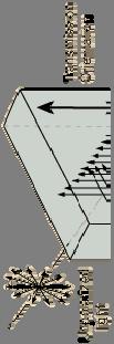

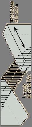
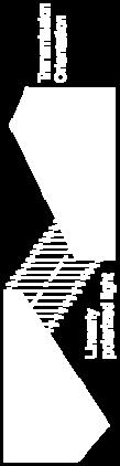
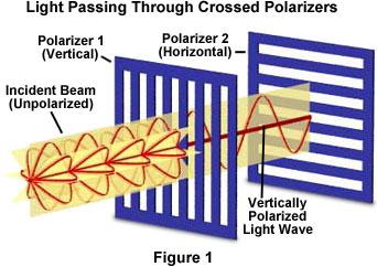
10 Crossed Polarizers ECE541/ME541 Microelectronic Fabrication Techniques Page 10
![Crystal polarizers (II) [birefringence] isotropic crystal (sodium](/docs-images/96/128799770/images/11-0.jpg "chloride) The 2 output beams are polarized (orthogonally).")
 ECE541/ME541 Microelectronic Fabrication")
11 Crystal polarizers (II) [birefringence] isotropic crystal (sodium chloride) The 2 output beams are polarized (orthogonally). anisotropic crystal (calcite) most stable polymorph of calcium carbonate (CaCO3) ECE541/ME541 Microelectronic Fabrication Techniques Page 11

12 ECE541/ME541 Microelectronic Fabrication Techniques Page 12
13 ECE541/ME541 Microelectronic Fabrication Techniques Page 13

14 ECE541/ME541 Microelectronic Fabrication Techniques Page 14
15 Ellipsometry Ohmic contacts I-V, C-V, Hall effect measurements Material Characterization PL, Raman, XRD, XPS, SIMS, EDX, etc ECE541/ME541 Microelectronic Fabrication Techniques Page 15
16 ECE541/ME541 Microelectronic Fabrication Techniques Page 16
17 ECE541/ME541 Microelectronic Fabrication Techniques Page 17

18 ECE541/ME541 Microelectronic Fabrication Techniques Page 18
19 ECE541/ME541 Microelectronic Fabrication Techniques Page 19

20 ECE541/ME541 Microelectronic Fabrication Techniques Page 20
21 ECE541/ME541 Microelectronic Fabrication Techniques Page 21
22 ECE541/ME541 Microelectronic Fabrication Techniques Page 22
23 ECE541/ME541 Microelectronic Fabrication Techniques Page 23

24 ECE541/ME541 Microelectronic Fabrication Techniques Page 24
25 ECE541/ME541 Microelectronic Fabrication Techniques Page 25

26 ECE541/ME541 Microelectronic Fabrication Techniques Page 26

27 ECE541/ME541 Microelectronic Fabrication Techniques Page 27
28 ECE541/ME541 Microelectronic Fabrication Techniques Page 28
29 Ellipsometry Ohmic contacts I-V, C-V, Hall effect measurements Material Characterization PL, Raman, XRD, XPS, SIMS, EDX, etc ECE541/ME541 Microelectronic Fabrication Techniques Page 29


30 Semiconductor device measurements setup 30 ECE541/ME541 Microelectronic Fabrication Techniques Page 30
31 I-V test setup Probe station Large working distance microscope Movable stage and platform Movable optics Movable electrical contacts Semiconductor Device Analyzer (SDA) 31 ECE541/ME541 Microelectronic Fabrication Techniques Page 31

32 Probe Station parts 32 ECE541/ME541 Microelectronic Fabrication Techniques Page 32

33 Micropositioners 33 ECE541/ME541 Microelectronic Fabrication Techniques Page 33
34 Probes 34 ECE541/ME541 Microelectronic Fabrication Techniques Page 34

35 Tips Metals used: Tungsten, Steel, Palladium, Osmium. 35 ECE541/ME541 Microelectronic Fabrication Techniques Page 35

36 Complete setup 36 ECE541/ME541 Microelectronic Fabrication Techniques Page 36

37 Semiconductor device analyzer 37 ECE541/ME541 Microelectronic Fabrication Techniques Page 37
38 I-V characteristic curve of Diode ECE541/ME541 Microelectronic Fabrication Techniques Page 38

39 What is Four Point Probing Four Point Probing is a method for measuring the resistivity of a substance. ECE541/ME541 Microelectronic Fabrication Techniques Page 39
40 How the system works In order to measure the resistivity of a substance, four points of contact must be made with the probe and the substance. Current goes through the two outer probes, and the difference in voltage is measured between the two inner probes. Through this process the resistance can be calculated. ECE541/ME541 Microelectronic Fabrication Techniques Page 40


41 Surface Resistivity In a regular three-dimensional conductor, the resistance can be written as where ρ is the resistivity, A is the cross-sectional area and L is the length. The cross-sectional area can be split into the width W and the sheet thickness t. By grouping the resistivity with the thickness, the resistance can then be written as: R s is then the sheet resistance. ECE541/ME541 Microelectronic Fabrication Techniques Page 41

42 High-accuracy capacitance measurements An AC signal of known frequency is applied through an internal low value resistor and the capacitor under test in a series configuration. The AC current flowing into the capacitor must also flow through the resistor, creating an AC voltage across the resistor. The magnitude and phase of this voltage can be measured and compared to the original AC signal, and the capacitance can be computed. Techniques such as this frequency domain measurement can be very accurate. LCR meter (Inductance (L), Capacitance (C), and Resistance (R)) ECE541/ME541 Microelectronic Fabrication Techniques Page 42


43 Tools for measurement Probe Station ECE541/ME541 Microelectronic Fabrication Techniques Page 43


44 Agilent Semiconductor Parameter Analyzer ECE541/ME541 Microelectronic Fabrication Techniques Page 44

45 Capacitance Voltage Measurements capacitance voltage (C-V) testing is to determine semiconductor parameters, particularly in MOSCAP and MOSFET structures. C-V measurements are also widely used to characterize other types of semiconductor devices and technologies, including bipolar junction transistors, JFETs, III-V compound devices, photovoltaic cells, MEMS devices, organic thin film transistor (TFT) displays, photodiodes, and carbon nanotubes (CNTs). Metal Oxide Silicon (MOS) capacitor ECE541/ME541 Microelectronic Fabrication Techniques Page 45
46 Capacitance Voltage Measurements C V measurements can reveal oxide thickness, oxide charges, contamination from mobile ions, and interface trap density in wafer processes. A deep depletion C V curves for an SiO2/Si MOS capacitor. NA = 1017 cm 3, t ox = 10 nm, A = cm 2. The capacitance is determined by superimposing a small amplitude ac voltage v on the dc voltage V. The ac voltage frequency is typically 10 khz to 1 MHz with 10 to 20 mv amplitude. ECE541/ME541 Microelectronic Fabrication Techniques Page 46

47 ECE541/ME541 Microelectronic Fabrication Techniques 47 Page 47
48 I Basic Physical Phenomena of Hall Effect When an electron moves in a direction perpendicular to an applied magnetic field, it experiences a force (Lorentz force) acting normal to both directions and moves in response to this force (see below for an n- type semiconductor) Constant current I (flows References: 2, 3. v e Lorentz Force F= ev x B F V V H B B V=0 Coordinate System d z y x along x axis) in the presence of magnetic field B (z axis) causes Lorentz force F (y axis) Causes electron paths to bend towards negative y axis Charge builds up on the surface of the side of sample, and the potential drop across the two sides of the sample is known as the Hall voltage (V H ) ECE541/ME541 Microelectronic Fabrication Techniques Page 48
49 When electrons flow without magnetic field... t semiconductor slice + _ I I d ECE541/ME541 Microelectronic Fabrication Techniques Page 49
50 When the magnetic field is turned on... I qbv B-field ECE541/ME541 Microelectronic Fabrication Techniques Page 50
51 As time goes by... high potential qe I qbv = qe low potential ECE541/ME541 Microelectronic Fabrication Techniques Page 51
52 Finally... V H I B-field ECE541/ME541 Microelectronic Fabrication Techniques Page 52


53 Basic Hall effect measurement system 53 ECE541/ME541 Microelectronic Fabrication Techniques Page 53
54 Ellipsometry Ohmic contacts I-V, C-V, Hall effect measurements Material Characterization PL, Raman, XRD, XPS, SIMS, EDX, etc (please also refer to Lecture 16, 17, and 25 for more details) ECE541/ME541 Microelectronic Fabrication Techniques Page 54
55 Photoluminescence Spectroscopy Continuum states Electronic bound state Laser energy E CB k h excitation h emission VB PL Intensity A laser excites electrons from the valence band into the conduction band, creating electron-hole pairs These electrons and holes recombine (annihilate) and emit a photon. The number of emitted photons (intensity) as a function of energy, which is photoluminescence (PL). ECE541/ME541 Microelectronic Fabrication Techniques Page 55

56 Discovery of Raman Spectroscopy In 1928, Raman discovered that the spectrum of scattered lines of CCl 4 liquid not only consisted of the Rayleigh lines but a pattern of lines of shifted frequency the Raman spectrum. Mr. Raman won the Nobel Prize of Physics in 1930, for his work on the scattering of light and for the discovery of the effect named after him. C.V. Raman ( ) ECE541/ME541 Microelectronic Fabrication Techniques Page 56
57 Stokes S Anti-Stokes S L q S L q S S L q ECE541/ME541 Microelectronic Fabrication Techniques Page 57 S L q
ME 432 Fundamentals of Modern Photovoltaics. Discussion 30: Contacts 7 November 2018
 ME 432 Fundamentals of Modern Photovoltaics Discussion 30: Contacts 7 November 2018 Fundamental concepts underlying PV conversion input solar spectrum light absorption carrier excitation & thermalization
Slide 1. Slide 2. Slide 3. Chapter 19: Electronic Materials. Learning Objectives. Introduction
 Slide 1 Chapter 19: Electronic Materials 19-1 Slide 2 Learning Objectives 1. Ohm s law and electrical conductivity 2. Band structure of solids 3. Conductivity of metals and alloys 4. Semiconductors 5.
the surface of a wafer, usually silicone. In this process, an oxidizing agent diffuses into the wafer
 Analysis of Oxide Thickness Measurement Techniques of SiO2: Nanometrics Nanospec Reflectometer and Color Chart Eman Mousa Alhajji North Carolina State University Department of Materials Science and Engineering
Crystallographic Characterization of GaN Nanowires by Raman Spectral Image Mapping
 Crystallographic Characterization of GaN Nanowires by Raman Spectral Image Mapping Heerad Farkhoor, Adam Schwartzberg, Jeffrey Urban August 12, 2009 Abstract Obtaining structural information of nano-structured
Supplementary Information
 Supplementary Information Supplementary Figure 1 Characterization of precursor coated on salt template. (a) SEM image of Mo precursor coated on NaCl. Scale bar, 50 μm. (b) EDS of Mo precursor coated on
Microelectronics Devices
 Microelectronics Devices Yao-Joe Yang 1 Outline Basic semiconductor physics Semiconductor devices Resistors Capacitors P-N diodes BJT/MOSFET 2 Type of Solid Materials Solid materials may be classified
Figure 16.31: Two-dimensional representations of (a) a quartz crystal and (b) a quartz glass.
 a quartz crystal and (b) a quartz glass.") Figure 16.31: Two-dimensional representations of (a) a quartz crystal and (b) a quartz glass. Figure 16.28: The p orbitals (a) perpendicular to the plane of th carbon ring system in graphite can combine
Figure 16.31: Two-dimensional representations of (a) a quartz crystal and (b) a quartz glass. Figure 16.28: The p orbitals (a) perpendicular to the plane of th carbon ring system in graphite can combine
HOMEWORK 4 and 5. March 15, Homework is due on Monday March 30, 2009 in Class. Answer the following questions from the Course Textbook:
 HOMEWORK 4 and 5 March 15, 2009 Homework is due on Monday March 30, 2009 in Class. Chapter 7 Answer the following questions from the Course Textbook: 7.2, 7.3, 7.4, 7.5, 7.6*, 7.7, 7.9*, 7.10*, 7.16, 7.17*,
Materials of Engineering ENGR 151 ELECTRCIAL PROPERTIES
 Materials of Engineering ENGR 151 ELECTRCIAL PROPERTIES ELECTRON ENERGY BAND STRUCTURES Atomic states split to form energy bands Adapted from Fig. 18.2, Callister & Rethwisch 9e. 2 BAND STRUCTURE REPRESENTATION
Ellipsometry as a tool for identifying process issues in roll-to-roll sputter deposited metal-oxide coatings
 Ellipsometry as a tool for identifying process issues in roll-to-roll sputter deposited metal-oxide coatings Sharon Louch Centre for Process Innovation, Wilton Centre, edcar. UK. TS10 3H Abstract Ellipsometry
ET3034TUx High efficiency concepts of c- Si wafer based solar cells
 ET3034TUx - 4.4 - High efficiency concepts of c- Si wafer based solar cells In the previous block we have discussed various technological aspects on crystalline silicon wafer based PV technology. In this
X-Ray Reflectivity Study of Hafnium Silicate Thin Films Prepared by Thermal Chemical Vapor Deposition
 X-Ray Reflectivity Study of Hafnium Silicate Thin Films Prepared by Thermal Chemical Vapor Deposition Hideyuki YAMAZAKI, Advanced LSI Technology Laboratory, Toshiba Corporation hideyuki.yamazaki@toshiba.co.jp
Characterization of Ga 2 O 3 Single Crystal and Thin Film
 Characterization of Ga 2 O 3 Single Crystal and Thin Film Emily Hommerding 8/27/2012 Abstract Ga 2 O 3 is a semiconductor with many yet unknown properties. Among its most interesting features are the fact
Supplementary Figure S1 Photograph of MoS 2 and WS 2 flakes exfoliated by different metal naphthalenide (metal = Na, K, Li), and dispersed in water.
, and dispersed in water.") Supplementary Figure S1 Photograph of MoS 2 and WS 2 flakes exfoliated by different metal naphthalenide (metal = Na, K, Li), and dispersed in water. Supplementary Figure S2 AFM measurement of typical LTMDs
Supplementary Figure S1 Photograph of MoS 2 and WS 2 flakes exfoliated by different metal naphthalenide (metal = Na, K, Li), and dispersed in water. Supplementary Figure S2 AFM measurement of typical LTMDs
Effect of annealing temperature on the electrical properties of HfAlO thin films. Chun Lia, Zhiwei Heb*
 International Forum on Energy, Environment and Sustainable Development (IFEESD 2016) Effect of annealing temperature on the electrical properties of HfAlO thin films Chun Lia, Zhiwei Heb* Department of
Nagatsuta, Midori-ku, Yokohama , Japan. Technology, 4259-S2-20 Nagatsuta, Midori-ku, Yokohama , Japan
 Improvement of Interface Properties of W/La O 3 /Si MOS Structure Using Al Capping Layer K. Tachi a, K. Kakushima b, P. Ahmet a, K. Tsutsui b, N. Sugii b, T. Hattori a, and H. Iwai a a Frontier Collaborative
Development of Silicon Pad and Strip Detector in High Energy Physics
 XXI DAE-BRNS High Energy Physics Symposium 2014, IIT Guwahati Development of Silicon Pad and Strip Detector in High Energy Physics Manoj Jadhav Department of Physics I.I.T. Bombay 2 Manoj Jadhav, IIT Bombay.
State of the art quality of a GeOx interfacial passivation layer formed on Ge(001)
") APPLICATION NOTE State of the art quality of a Ox interfacial passivation layer formed on (001) Summary A number of research efforts have been made to realize Metal-Oxide-Semiconductor Field Effect Transistors
APPLICATION NOTE State of the art quality of a Ox interfacial passivation layer formed on (001) Summary A number of research efforts have been made to realize Metal-Oxide-Semiconductor Field Effect Transistors
Ion Implantation Most modern devices doped using ion implanters Ionize gas sources (single +, 2+ or 3+ ionization) Accelerate dopant ions to very
 Accelerate dopant ions to very") Ion Implantation Most modern devices doped using ion implanters Ionize gas sources (single +, 2+ or 3+ ionization) Accelerate dopant ions to very high voltages (10-600 KeV) Use analyzer to selection charge/mass
Ion Implantation Most modern devices doped using ion implanters Ionize gas sources (single +, 2+ or 3+ ionization) Accelerate dopant ions to very high voltages (10-600 KeV) Use analyzer to selection charge/mass
High Transmittance Ti doped ITO Transparent Conducting Layer Applying to UV-LED. Y. H. Lin and C. Y. Liu
 High Transmittance Ti doped ITO Transparent Conducting Layer Applying to UV-LED Y. H. Lin and C. Y. Liu Department of Chemical Engineering and Materials Engineering, National Central University, Jhongli,
Supporting Information. Solution-Processed 2D PbS Nanoplates with Residual Cu 2 S. Exhibiting Low Resistivity and High Infrared Responsivity
 Supporting Information Solution-Processed 2D PbS Nanoplates with Residual Cu 2 S Exhibiting Low Resistivity and High Infrared Responsivity Wen-Ya Wu, Sabyasachi Chakrabortty, Asim Guchhait, Gloria Yan
The Effect of Annealing on Resistivity Measurements of TiSi 2 and TiN Using the collinear Four Point Probe Technique
 The Effect of Annealing on Resistivity Measurements of TiSi 2 and TiN Using the collinear Four Point Probe Technique Eman Mousa Alhajji North Carolina State University Department of Materials Science and
High Speed Devices and Circuits Prof K. N. Bhat Department of Electrical Engineering Indian Institute of Technology, Madras
 High Speed Devices and Circuits Prof K. N. Bhat Department of Electrical Engineering Indian Institute of Technology, Madras Lecture 4 Ternary Compound Semiconductors and their Applications Last time we
Plasma Etching Rates & Gases Gas ratios affects etch rate & etch ratios to resist/substrate
 Plasma Etching Rates & Gases Gas ratios affects etch rate & etch ratios to resist/substrate Development of Sidewalls Passivating Films Sidewalls get inert species deposited on them with plasma etch Creates
PHYSICSOF SOLARCELLS. Jenny Nelson. Imperial College, UK. Imperial College Press ICP
 im- PHYSICSOF SOLARCELLS Jenny Nelson Imperial College, UK ICP Imperial College Press Contents Preface v Chapter 1 Introduction 1 1.1. Photons In, Electrons Out: The Photovoltaic Effect 1 1.2. Brief History
Physical Vapor Deposition (PVD) Zheng Yang
 Zheng Yang") Physical Vapor Deposition (PVD) Zheng Yang ERF 3017, email: yangzhen@uic.edu Page 1 Major Fabrication Steps in MOS Process Flow UV light Mask oxygen Silicon dioxide photoresist exposed photoresist oxide
Physical Vapor Deposition (PVD) Zheng Yang ERF 3017, email: yangzhen@uic.edu Page 1 Major Fabrication Steps in MOS Process Flow UV light Mask oxygen Silicon dioxide photoresist exposed photoresist oxide
IC Fabrication Technology Part III Devices in Semiconductor Processes
 EE 330 Lecture 10 IC Fabrication Technology Part III Metalization and Interconnects Parasitic Capacitances Back-end Processes Devices in Semiconductor Processes Resistors Diodes Review from Last Lecture
Light Emission Analysis of Trench Gate Oxides of Power Devices
 Special Issue Recent R&D Activities of Power Devices for Hybrid ElectricVehicles 17 Research Report Light Emission Analysis of Trench Gate Oxides of Power Devices Masanori Usui, Takahide Sugiyama, Masayasu
2007 IEEE International Conference on Electron Devices and Solid-State Circuits
 Proceedings 2007 IEEE International Conference on Electron Devices and Solid-State Circuits ~ December 20-22, 2007 Tayih Landis Hotel, Tainan, Taiwan Volume I Aluminium Incorporation in Lanthanum Oxide
EE 330 Lecture 9. IC Fabrication Technology Part II. -Oxidation -Epitaxy -Polysilicon -Planarization -Resistance and Capacitance in Interconnects
 EE 330 Lecture 9 IC Fabrication Technology Part II -Oxidation -Epitaxy -Polysilicon -Planarization -Resistance and Capacitance in Interconnects Review from Last Time Etching Dry etch (anisotropic) SiO
Influence of oxygen to argon ratio on the optical and structural properties of rf magnetron sputtered Ba 0.7 Sr 0.3 TiO 3 thin films.
 Chapter 4 Influence of oxygen to argon ratio on the optical and structural properties of rf magnetron sputtered Ba 0.7 Sr 0.3 TiO 3 thin films. The optical properties of barium strontium titanate thin
More on oxidation. Oxidation systems Measuring oxide thickness Substrate orientation Thin oxides Oxide quality Si/SiO2 interface Hafnium oxide
 More on oxidation Oxidation systems Measuring oxide thickness Substrate orientation Thin oxides Oxide quality Si/SiO2 interface Hafnium oxide EE 432/532 oxide measurements, etc 1 Oxidation systems silicon
Influence of the oxide thickness on the magnetic properties of Fe/ FeO multilayers.
 DESY Summer Student Program Influence of the oxide thickness on the magnetic properties of Fe/ FeO multilayers. Student: Guryeva Tatyana Supervisors: Ralf Röhlsberger Kai Schlage Sebastien Couet Hamburg,
Nanotechnology Activities in Korea
 Nanotechnology Activities in Korea Hee-Gook Lee President LG Electronics, Inc. CONTENTS I. National Programs Industry Academia NTRA II. Summaries Overview of Korean Approach Korean environments and the
General Introduction to Microstructure Technology p. 1 What is Microstructure Technology? p. 1 From Microstructure Technology to Microsystems
 General Introduction to Microstructure Technology p. 1 What is Microstructure Technology? p. 1 From Microstructure Technology to Microsystems Technology p. 9 The Parallels to Microelectronics p. 15 The
Semiconductor Technology
 Semiconductor Technology from A to Z Oxidation www.halbleiter.org Contents Contents List of Figures List of Tables II III 1 Oxidation 1 1.1 Overview..................................... 1 1.1.1 Application...............................
Photovoltaic Fundamentals, Technology and Practice Dr. Mohamed Fawzy Aboud Sustainable Energy Technologies center (SET)
") Photovoltaic Fundamentals, Technology and Practice Dr. Mohamed Fawzy Aboud Sustainable Energy Technologies center (SET) The Greenhouse Effect 270 ppm carbon dioxide (CO 2 ) in the atmosphere absorbs outgoing
Photovoltaic Fundamentals, Technology and Practice Dr. Mohamed Fawzy Aboud Sustainable Energy Technologies center (SET) The Greenhouse Effect 270 ppm carbon dioxide (CO 2 ) in the atmosphere absorbs outgoing
Thermal Evaporation. Theory
 Thermal Evaporation Theory 1. Introduction Procedures for depositing films are a very important set of processes since all of the layers above the surface of the wafer must be deposited. We can classify
Growth of Gate Oxides on 4H SiC by NO at Low Partial Pressures
 Growth of Gate Oxides on 4H SiC by NO at Low Partial Pressures Author Haasmann, Daniel, Dimitrijev, Sima, Han, Jisheng, Iacopi, Alan Published 214 Journal Title Materials Science Forum DOI https://doi.org/1.428/www.scientific.net/msf.778-78.627
Development of High Voltage Silicon Carbide MOSFET Devices in KERI
 Development of High Voltage Silicon Carbide MOSFET Devices in KERI 2014. 06. Kim, Sang Cheol (sckim@keri.re.kr) Power Semiconductor Device Research Center Korea Electrotechnology Research Institute Contents
Plasma Etching Rates & Gases Gas ratios affects etch rate & etch ratios to resist/substrate
 Plasma Etching Rates & Gases Gas ratios affects etch rate & etch ratios to resist/substrate Development of Sidewalls Passivating Films Sidewalls get inert species deposited on them with plasma etch Creates
Fairchild Semiconductor Application Note June 1983 Revised March 2003
 Fairchild Semiconductor Application Note June 1983 Revised March 2003 High-Speed CMOS (MM74HC) Processing The MM74HC logic family achieves its high speed by utilizing microcmos Technology. This is a 3.5
From microelectronics down to nanotechnology.
 From microelectronics down to nanotechnology sami.franssila@tkk.fi Contents Lithography: scaling x- and y-dimensions MOS transistor physics Scaling oxide thickness (z-dimension) CNT transistors Conducting
ECE 541/ME 541 Microelectronic Fabrication Techniques
 ECE 541/ME 541 Microelectronic Fabrication Techniques MW 4:00-5:15 pm Introduction to Vacuum Technology Zheng Yang ERF 3017, email: yangzhen@uic.edu ECE541/ME541 Microelectronic Fabrication Techniques
NONTRADITIONAL MANUFACTURING PROCESSES
 NONTRADITIONAL MANUFACTURING PROCESSES Lasers & Laser Beam Machining Basic NTM Process Groups: * Thermal NTM Processes - Laser Beam Machining (LBM) - Electron Beam Machining (EBM) - Plasma Arc Machining
How can we describe a crystal?
 How can we describe a crystal? Examples of common structures: (1) The Sodium Chloride (NaCl) Structure (LiH, MgO, MnO, AgBr, PbS, KCl, KBr) The NaCl structure is FCC The basis consists of one Na atom and
Nano-Solar - A Technique for Optimal Usage of Solar Energy
 Nano-Solar - A Technique for Optimal Usage of Solar Energy HARISH THUTUPALLI Electronics and Instrumentation engineering, CVR College of Engineering, Hyderabad-501510, AP, India. E.Mail: harish.endeavour.fluky@gmail.com
Surface plasmon enhanced emission from dye doped polymer layers
 Surface plasmon enhanced emission from dye doped polymer layers Terrell D. Neal, a) Koichi Okamoto, and Axel Scherer Department of Electrical Engineering, California Institute of Technology, Pasadena,
Oxide Growth. 1. Introduction
 Oxide Growth 1. Introduction Development of high-quality silicon dioxide (SiO2) has helped to establish the dominance of silicon in the production of commercial integrated circuits. Among all the various
Energy & Sustainability
 Energy & Sustainability Lecture 24: Renewable Energy April 23, 2009 Renewable Energy Sources Solar the mother of all renewables Direct solar plus wind and wave power, hydroelectricity and biomass (indirect
Carbon nanostructures. (http://www.mf.mpg.de/de/abteilungen/schuetz/index.php?lang=en&content=researchtopics&type=specific&name=h2storage)
") Carbon nanostructures (http://www.mf.mpg.de/de/abteilungen/schuetz/index.php?lang=en&content=researchtopics&type=specific&name=h2storage) 1 Crystal Structures Crystalline Material: atoms arrange into a
Carbon nanostructures (http://www.mf.mpg.de/de/abteilungen/schuetz/index.php?lang=en&content=researchtopics&type=specific&name=h2storage) 1 Crystal Structures Crystalline Material: atoms arrange into a
350 C for 8 hours in argon atmosphere. Supplementary Figures. Supplementary Figure 1 High-temperature annealing of BP flakes on SiO 2.
 Supplementary Figures Supplementary Figure 1 High-temperature annealing of BP flakes on SiO 2. (a-d) The optical images of three BP flakes on a SiO 2 substrate before (a,b) and after annealing (c,d) at
INVESTIGATION OF PHOTOVOLTAIC PROPERTIES of p-inse/n-cds HETEROJUNCTION SOLAR CELLS
 Journal of Ovonic Research Vol. 1, No. 3, May - June 214, p. 67-73 INVESTIGATION OF PHOTOVOLTAIC PROPERTIES of p-inse/n-cds HETEROJUNCTION SOLAR CELLS K. YILMAZ * Pamukkale University, Science and Arts
CHAPTER 5. ABSORPTION AND FLUORESCENCE OF CsI(Tl) AND. CsI(Tl)In CRYSTALS
 AND. CsI(Tl)In CRYSTALS") CHAPTER 5 ABSORPTION AND FLUORESCENCE OF CsI(Tl) AND CsI(Tl)In CRYSTALS 93 ABSTRACT In order to obtain a laser action in doped alkali halides crystals, fluorescence measurements have been performed in
CHAPTER 5 ABSORPTION AND FLUORESCENCE OF CsI(Tl) AND CsI(Tl)In CRYSTALS 93 ABSTRACT In order to obtain a laser action in doped alkali halides crystals, fluorescence measurements have been performed in
Sensor. Device that converts a non-electrical physical or chemical quantity into an electrical signal. Sensor Processor Display Output signal
 Microsensors Outline Sensor & microsensor Force and pressure microsensors Position and speed microsensors Acceleration microsensors Chemical microsensors Biosensors Temperature sensors Sensor Device that
DESIGN AND OPERATING PRINCIPLES OF III- V SOLAR CELLS
 DESIGN AND OPERATING PRINCIPLES OF III- V SOLAR CELLS ANTHONY MELECO CAPSTONE ADVISER: DR. IAN SELLERS TABLE OF CONTENTS Abstract... 3 Introduction... 3 Procedure... 4 Photomask... 4 Modeling... 5 IV curve...
Rational defect passivation of Cu 2 ZnSn(S,Se) 4 photovoltaics with solution-processed Cu 2 ZnSnS 4 :Na nanocrystals
 4 photovoltaics with solution-processed Cu 2 ZnSnS 4 :Na nanocrystals") Supporting Information for Rational defect passivation of Cu 2 ZnSn(S,Se) 4 photovoltaics with solution-processed Cu 2 ZnSnS 4 :Na nanocrystals Huanping Zhou 1,2+, Tze-Bin Song 1,2+, Wan-Ching Hsu 1,2,
Supporting Information for Rational defect passivation of Cu 2 ZnSn(S,Se) 4 photovoltaics with solution-processed Cu 2 ZnSnS 4 :Na nanocrystals Huanping Zhou 1,2+, Tze-Bin Song 1,2+, Wan-Ching Hsu 1,2,
Amorphous Silicon Solar Cells
 The Birnie Group solar class and website were created with much-appreciated support from the NSF CRCD Program under grants 0203504 and 0509886. Continuing Support from the McLaren Endowment is also greatly
Manufacturing Technologies for MEMS and SMART SENSORS
 4 Manufacturing Technologies for MEMS and SMART SENSORS Dr. H. K. Verma Distinguished Professor (EEE) Sharda University, Greater Noida (Formerly: Deputy Director and Professor of Instrumentation Indian
Process Development for Porous Silicon Light-Emitting Devices
 Process Development for Porous Silicon Light-mitting Devices Jason Benz Advisor: K. Hirschman Rochester Institute of Technology Rochester, NY 14623 Absfract - The primary focus of this project was to continue
Biophotonics. Light Matter Interactions & Lasers. NPTEL Biophotonics 1
 Biophotonics Light Matter Interactions & Lasers NPTEL Biophotonics 1 Overview In this lecture you will learn, Light matter interactions: absorption, emission, stimulated emission Lasers and some laser
Introduction to Lithography
 Introduction to Lithography G. D. Hutcheson, et al., Scientific American, 290, 76 (2004). Moore s Law Intel Co-Founder Gordon E. Moore Cramming More Components Onto Integrated Circuits Author: Gordon E.
TOWARD MEMS!Instructor: Riadh W. Y. Habash
 TOWARD MEMS!Instructor: Riadh W. Y. Habash Students are presented with aspects of general production and manufacturing of integrated circuit (IC) products to enable them to better liaise with and participate
EE 330 Lecture 9. IC Fabrication Technology Part 2
 EE 330 Lecture 9 IC Fabrication Technology Part 2 Quiz 8 A 2m silicon crystal is cut into wafers using a wire saw. If the wire diameter is 220um and the wafer thickness is 350um, how many wafers will this
Lecture 22: Integrated circuit fabrication
 Lecture 22: Integrated circuit fabrication Contents 1 Introduction 1 2 Layering 4 3 Patterning 7 4 Doping 8 4.1 Thermal diffusion......................... 10 4.2 Ion implantation.........................
ALD of Scandium Oxide from Tris(N,N -diisopropylacetamidinato)scandium and Water
scandium and Water") ALD of Scandium Oxide from Tris(N,N -diisopropylacetamidinato)scandium and Water Philippe P. de Rouffignac, Roy G. Gordon Dept. of Chemistry,, Cambridge, MA gordon@chemistry.harvard.edu (617) 495-4017
ALD of Scandium Oxide from Tris(N,N -diisopropylacetamidinato)scandium and Water Philippe P. de Rouffignac, Roy G. Gordon Dept. of Chemistry,, Cambridge, MA gordon@chemistry.harvard.edu (617) 495-4017
Microelectronics. Integrated circuits. Introduction to the IC technology M.Rencz 11 September, Expected decrease in line width
 Microelectronics Introduction to the IC technology M.Rencz 11 September, 2002 9/16/02 1/37 Integrated circuits Development is controlled by the roadmaps. Self-fulfilling predictions for the tendencies
Silver Diffusion Bonding and Layer Transfer of Lithium Niobate to Silicon
 Chapter 5 Silver Diffusion Bonding and Layer Transfer of Lithium Niobate to Silicon 5.1 Introduction In this chapter, we discuss a method of metallic bonding between two deposited silver layers. A diffusion
Low-cost, deterministic quasi-periodic photonic structures for light trapping in thin film silicon solar cells
 Low-cost, deterministic quasi-periodic photonic structures for light trapping in thin film silicon solar cells The MIT Faculty has made this article openly available. Please share how this access benefits
Contents. From microelectronics down to nanotechnology
 Contents From microelectronics down to nanotechnology sami.franssila@tkk.fi Lithography: scaling x- and y-dimensions MOS transistor physics Scaling oxide thickness (z-dimension) CNT transistors Conducting
Contents. From microelectronics down to nanotechnology. Top down nanotechnology. Writing patterns
 Contents From microelectronics down to nanotechnology sami.franssila@tkk.fi Lithography: scaling x- and y-dimensions MOS transistor physics Scaling oxide thickness (z-dimension) CNT transistors Conducting
EE 330 Lecture 9. IC Fabrication Technology Part II. -Oxidation -Epitaxy -Polysilicon -Planarization -Resistance and Capacitance in Interconnects
 EE 330 Lecture 9 IC Fabrication Technology Part II -Oxidation -Epitaxy -Polysilicon -Planarization -Resistance and Capacitance in Interconnects Review from Last Time IC Fabrication Technology Crystal Preparation
ECE280: Nano-Plasmonics and Its Applications. Week5. Extraordinary Optical Transmission (EOT)
") ECE280: Nano-Plasmonics and Its Applications Week5 Extraordinary Optical Transmission (EOT) Introduction Sub-wavelength apertures in metal films provide light confinement beyond the fundamental diffraction
ECE280: Nano-Plasmonics and Its Applications Week5 Extraordinary Optical Transmission (EOT) Introduction Sub-wavelength apertures in metal films provide light confinement beyond the fundamental diffraction
FABRICATION ENGINEERING MICRO- NANOSCALE ATTHE AND. Fourth Edition STEPHEN A. CAMPBELL. of Minnesota. University OXFORD UNIVERSITY PRESS
 AND FABRICATION ENGINEERING ATTHE MICRO- NANOSCALE Fourth Edition STEPHEN A. CAMPBELL University of Minnesota New York Oxford OXFORD UNIVERSITY PRESS CONTENTS Preface xiii prrt i OVERVIEW AND MATERIALS
A discussion of crystal growth, lithography, etching, doping, and device structures is presented in
 Chapter 5 PROCESSING OF DEVICES A discussion of crystal growth, lithography, etching, doping, and device structures is presented in the following overview gures. SEMICONDUCTOR DEVICE PROCESSING: AN OVERVIEW
Project III. 4: THIN FILM DEVICES FOR LARGE AREA ELECTRONICS
 Project III. 4: THIN FILM DEVICES FOR LARGE AREA ELECTRONICS Project leader: Dr D.N. Kouvatsos Collaborating researchers from other projects: Dr D. Davazoglou Ph.D. candidates: M. Exarchos, L. Michalas
Measurement of thickness of native silicon dioxide with a scanning electron microscope
 Measurement of thickness of native silicon dioxide with a scanning electron microscope V. P. Gavrilenko* a, Yu. A. Novikov b, A. V. Rakov b, P. A. Todua a a Center for Surface and Vacuum Research, 40 Novatorov
Chemically Tunable Full Spectrum Optical Properties of 2D Silicon Telluride Nanoplates
 SUPPORTING INFORMATION Chemically Tunable Full Spectrum Optical Properties of 2D Silicon Telluride Nanoplates Mengjing Wang,, Gabriella Lahti, David Williams, and Kristie J. Koski * Department of Chemistry,
Properties of Materials
 Properties of Materials Thermal Properties Thermal Conductivity Temperature Wall The Thermal Conductivity (k) is the measure of the ability of a material to transmit heat by conduction. The heat (Q) is
EECS130 Integrated Circuit Devices
 EECS130 Integrated Circuit Devices Professor Ali Javey 9/13/2007 Fabrication Technology Lecture 1 Silicon Device Fabrication Technology Over 10 15 transistors (or 100,000 for every person in the world)
Excitation and pressure effects on photoluminescence from silicon-based light emitting diode material
 Excitation and pressure effects on photoluminescence from silicon-based light emitting diode material Y. Ishibashi 1,3, A. Nagata 1, T. Kobayashi 1 *, A.D. Prins 2, S. Sasahara 3, J. Nakahara 3, M.A. Lourenco
Introduction to Polymer-Dispersed Liquid Crystals
 Introduction to Polymer-Dispersed Liquid Crystals Polymer-dispersed liquid crystals (PDLCs) are a relatively new class of materials that hold promise for many applications ranging from switchable windows
ECE440 Nanoelectronics. Lecture 08 Review of Solid State Physics
 ECE440 Nanoelectronics Lecture 08 Review of Solid State Physics A Brief review of Solid State Physics Crystal lattice, reciprocal lattice, symmetry Crystal directions and planes Energy bands, bandgap Direct
Crystalline Silicon Solar Cells With Two Different Metals. Toshiyuki Sameshima*, Kazuya Kogure, and Masahiko Hasumi
 Crystalline Silicon Solar Cells With Two Different Metals Toshiyuki Sameshima*, Kazuya Kogure, and Masahiko Hasumi Tokyo University of Agriculture and Technology, 2-24-16 Naka-cho, Koganei, Tokyo 184-8588,
Exam 1 Friday Sept 22
 Exam 1 Friday Sept 22 Students may bring 1 page of notes Next weeks HW assignment due on Wed Sept 20 at beginning of class No 5:00 p.m extension so solutions can be posted Those with special accommodation
Er 3+ Photoluminescence Excitation Spectra in Erbium-Doped Epitaxial Silicon Structures
 Physics of the Solid State, Vol. 46, No. 1, 24, pp. 97 1. Translated from Fizika Tverdogo Tela, Vol. 46, No. 1, 24, pp. 98 11. Original Russian Text Copyright 24 by Andreev, Krasil nik, Kryzhkov, Yablonskiœ,
Low temperature deposition of thin passivation layers by plasma ALD
 1 Low temperature deposition of thin passivation layers by plasma ALD Bernd Gruska, SENTECH Instruments GmbH, Germany 1. SENTECH in brief 2. Low temperature deposition processes 3. SENTECH SI ALD LL System
The next thin-film PV technology we will discuss today is based on CIGS.
 ET3034TUx - 5.3 - CIGS PV Technology The next thin-film PV technology we will discuss today is based on CIGS. CIGS stands for copper indium gallium selenide sulfide. The typical CIGS alloys are heterogeneous
THIN METALLIC LAYERS STRUCTURED BY E-BEAM LITHOGRAPHY. Miroslav HORÁČEK, Vladimír KOLAŘÍK, Michal URBÁNEK, František MATĚJKA, Milan MATĚJKA
 THIN METALLIC LAYERS STRUCTURED BY E-BEAM LITHOGRAPHY Miroslav HORÁČEK, Vladimír KOLAŘÍK, Michal URBÁNEK, František MATĚJKA, Milan MATĚJKA Ústav přístrojové techniky AV ČR, v. v. i., Královopolská 147,
Passivation of SiO 2 /Si Interfaces Using High-Pressure-H 2 O-Vapor Heating
 Jpn. J. Appl. Phys. Vol. 39 (2000) pp. 2492 2496 Part, No. 5A, May 2000 c 2000 The Japan Society of Applied Physics Passivation of O 2 / Interfaces Using High-Pressure-H 2 O-Vapor Heating Keiji SAKAMOTO
High-Resolution, Electrohydrodynamic Inkjet Printing of Stretchable, Metal Oxide Semiconductor Transistors with High Performances
 Electronic Supplementary Material (ESI) for Nanoscale. This journal is The Royal Society of Chemistry 2016 ` Electronic Supplementary Information High-Resolution, Electrohydrodynamic Inkjet Printing of
Supplementary Figure 1. (a-d). SEM images of h-bn film on iron foil with corresponding Raman spectra. Iron foil was reused for re-growth of h-bn
. SEM images of h-bn film on iron foil with corresponding Raman spectra. Iron foil was reused for re-growth of h-bn") Supplementary Figure 1. (a-d). SEM images of h-bn film on iron foil with corresponding Raman spectra. Iron foil was reused for re-growth of h-bn after bubbling transfer. Scale bars (ad) 20 μm. Supplementary
Supplementary Figure 1. (a-d). SEM images of h-bn film on iron foil with corresponding Raman spectra. Iron foil was reused for re-growth of h-bn after bubbling transfer. Scale bars (ad) 20 μm. Supplementary
Summary and Scope for further study
 Chapter 6 Summary and Scope for further study 6.1 Summary of the present study Transparent electronics is an emerging science and technology field concentrated on fabricating invisible electronic circuits
Laser Processing and Characterisation of 3D Diamond Detectors
 Laser Processing and Characterisation of 3D Diamond Detectors ADAMAS GSI meeting 3rd Dec 2015 Steven Murphy University of Manchester 3D Diamond Group / RD42 Outline Laser setup for fabricating graphitic
Chapter 22: Optical Properties
 Chapter 22: Optical Properties ISSUES TO ADDRESS... What phenomena occur when light is shined on a material? What determines the characteristic colors of materials? Why are some materials transparent and
Characterisation of Fe-Ni amorphous thin films for possible magnetostrictive sensor applications
 Characterisation of Fe-Ni amorphous thin films for possible magnetostrictive sensor applications Contents 9.1 Introduction 9.2 Experiment 9.3 Results and Discussions 9.4 Conclusion 9.1 Introduction Magnetostrictive
Red luminescence from Si quantum dots embedded in SiO x films grown with controlled stoichiometry
 Red luminescence from Si quantum dots embedded in films grown with controlled stoichiometry Zhitao Kang, Brannon Arnold, Christopher Summers, Brent Wagner Georgia Institute of Technology, Atlanta, GA 30332
TABLE OF CONTENTS DECLARATION DEDICATION ACKNOWLEDGEMENTS ABSTRACT ABSTRAK TABLE OF CONTENTS LIST OF TABLES LIST OF FIGURES LIST OF SYMBOLS
 v ABSTRACT A study of optical properties of Diamond-like Carbon Thin Films deposited by DC-PECVD. The films was deposited on the corning with the ratio of Hydrogen, H 2 (97%) and Methane, CH 4 (3%). The
Fabrication of photonic band-gap crystals
 Fabrication of photonic band-gap crystals C. C. Cheng and A. Scherer California Institute of Technology, Pasadena, California 91125 Received 19 June 1995; accepted 9 August 1995 We describe the fabrication
Observation in the GB (Gentle Beam) Capabilities
 Capabilities") A field-emission cathode in the electron gun of a scanning electron microscope provides narrower probing beams at low as well as high electron energy, resulting in both improved spatial resolution and
A field-emission cathode in the electron gun of a scanning electron microscope provides narrower probing beams at low as well as high electron energy, resulting in both improved spatial resolution and