Nanoimprinting. Nanoimprint. Spin Coating Imprinting De-molding Etching
|
|
|
- Rosaline Atkinson
- 6 years ago
- Views:
Transcription
1 Nanoimprinting Nanoimprint Spin Coating Imprinting De-molding Etching 1
 http://www.microresist.de/thermoplastic_en.")
2 Nanoimprint Glass Transition Temperatures (Tg) mr-i C mr-i C mr-i PMMA 105 C 2


3 10 nm holes 10 nm holes and 40 nm pitch in PMMA fabricated by nanoimprint lithography Micro- and Nanoimprint C C Chang et. al, A Study of The Thin Film Heat Transfer in a Rapid-heating Nanoimprint Process, EMN04, October 2004, Paris, France 3


4 Rolling Imprint Step and Stamp Imprint Lithography,SSIL University of Texas at Austin, USA 4

 使低黏度光阻硬化成形 Lithography 5")
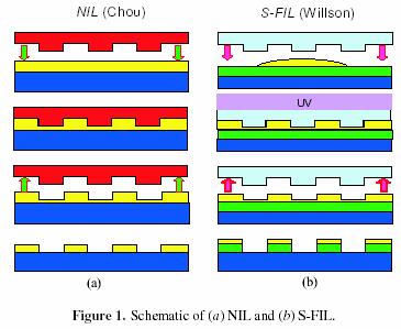
5 Step and Flash Imprint Lithography,SFIL 發展常溫常壓下的微影轉印製程 採小面積步進轉印微影紫外光 (UV) 使低黏度光阻硬化成形 Step and Flash Imprint Lithography 5


6 Large scale ultraviolet-based nanoimprint lithography, B. Vratzov, A. Fuchs, M. Lemme, W. Henschel, and H. Kurz, J. Vac. Sci. Technol. B Vol 21, No 6, Nov Dec 2003, Large scale ultraviolet-based nanoimprint lithography, B. Vratzov, A. Fuchs, M. Lemme, W. Henschel, and H. Kurz, J. Vac. Sci. Technol. B Vol 21, No 6, Nov Dec 2003,

7 Microcontact Print, μ-cp (Soft Lithography) PDMS ( 聚二甲基矽氧烷 ) Thiol ( 一種有機高分子硫醇 ) Gold thin file + Thiol Self-Assembly Monolayer, SAM Bottom-up Approach Y. Xia, G. M. Whitesides, Angew. Chem. Int. Vol.37, pp , 1998, Laser-Assisted Direct Imprint, LADI 利用雷射加熱矽基材直接壓印的雷射輔助直接壓印 7


8 Laser-Assisted Direct Imprint, LADI SEM image of the cross-section of samples patterned using LADI. a, A quartz mould. b, Imprinted patterns in silicon. The imprinted silicon grating is 140 nm wide, 110 nm deep and has a 300 nm period, an inverse of the mould. Fabrication of 70 nm channel length polymer organic thin-film transistors using nanoimprint lithography Michael D. Austina and Stephen Y. Chou, APPLIED PHYSICS LETTERS, VOLUME 81, NUMBER 23 2 DECEMBER 2002 OTFT device 於塑膠基板上, 利用高精度印刷技術製作 P- 型與 N 型有機薄膜電晶體 Using precision printing technology to fabricate p type and N type organic TFT on plastic substrate 應用範圍 : 軟性顯示器 軟性有機電子元件 8
9 ITRI Project EVG s Nanoimprint Lithography Products Hot Embossing Micro Contact Printing UV-Nanoimprint Lithography 9

10 Equipment Developers EV Group (EVG) SUSS MicroTec Obducat EVG s Nanoimprint Products EVG520HE The EVG520HE semi-automated hot embossing system is designed for embossing and nanoimprinting applications. This productionproven system from EVG accepts substrates up to 200 mm and is compatible with standard semiconductor manufacturing technologies. The hot embossing system is configured with a universal embossing chamber, high-vacuum and high-contact force capabilities and manages the whole range of polymers suitable for hot embossing. Together with high-aspect ratio embossing and multiple de-embossing options many processes for high quality pattern transfer and nm resolution are offered. 10

 no ink is deposited.")
11 Dip-Pen Nanolithography Transport of molecules to the surface via water meniscus( 凹面 ) Dip-pen nanolithography heats up with new technique Diagram illustrating thermal dip pen nanolithography. When the cantilever is cold (left) no ink is deposited. When the cantilever is heated (right), the ink melts and is deposited onto the surface. Source: Naval Research Laboratory 11


12 DPN Kit - DPN Pens & Substrates DPN Substrates - patterned alignment oxide-sharpened DPN probe tips DPN Probes singles triples as many W D L D L A W A Wafer Type 1 Wafer Types 2 &


13 DPN Pens NSCRIPTOR user interface leverages InkCAD CAD to create nanoscale patterns 13


14 NSCRIPTOR DPNWriter DPN InkWells 14
 R123 R141.")
15 Dip-Pen Nanolithography Possible applications Recent progress in nanoimprint technology and its applications L Jay Guo, Recent progress in nanoimprint technology and its applications, Journal Of Physics D: Applied Physics, 37 (2004) R123 R
16 16
17 17


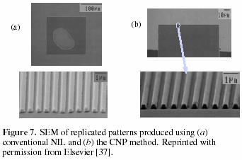
18 CNP: Combined nanoimprint and photolithography 18

19 19

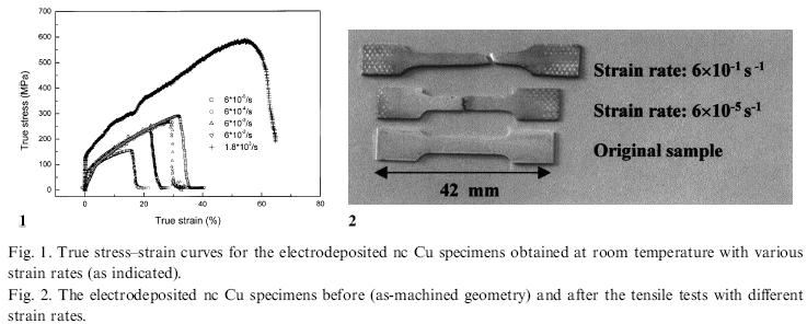
20 20
21 21

22 22
23 23

24 24
25 25
26 Nanostructing Techniques Severe Plastic Deformation (SPD) 26

27 Severe Plastic Deformation (SPD) Special set-up of thermomechanical processing Rolling Wire-drawing Extrusion High reduction rates or with a combination of different steps during cold deformation Equal Channel Angular Processing (ECAP) 27
28 Equal Channel Angular Processing (ECAP) It is shown that simple shear can be considered as a near ideal deformation method for structure and texture formation in metalworking. It has the advantage of producing extra-large, strictly uniform and unidirectional deformations under relatively low pressure and load. Without macroscopic shape change Equal Channel Angular Processing (ECAP) There are many potential and promising applications of this deformation method in materials synthesis and processing. It should be pointed out that breakdown of cast ingots, consolidation and bonding of powders and grain refinement by ECAP with subsequent recrystallisation treatments can be used to produce submicron-grained structures in various materials. The process can easily be repeated a number of times in the same tool. The process can also be extended from Extrusion to Drawing. 28

29 Grain Size Grain Size 29
")

30 Accumulative Roll Bonding (ARB) Accumulative Roll Bonding (ARB) Aluminum 30
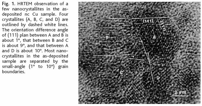
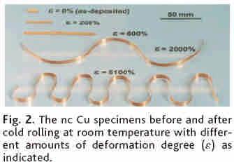
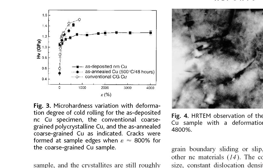
31 Nanocrystalline Copper Superplastic Extensibility of Nanocrystalline Copper at Room Temperature L. Lu, M. L. Sui, K. Lu1 SCIENCE VOL FEBRUARY 2000 A bulk nanocrystalline (nc) pure copper with high purity and high density was synthesized by electrodeposition. An extreme extensibility (elongation exceeds 5000%) without a strain hardening effect was observed when the nc copper specimen was rolled at room temperature. Microstructure analysis suggests that the superplastic extensibility of the nc copper originates from a deformation mechanism dominated by grain boundary activities rather than lattice dislocation, which is also supported by tensile creep studies at room temperature. This behavior demonstrates new possibilities for scientic and technological advancements with nc materials. 31

32 32
33 33

34 34
 942 948 Surface mechanical attrition treatment (SMAT) was employed to fabricate a nanocrystalline surface layer on a pure copper plate.")
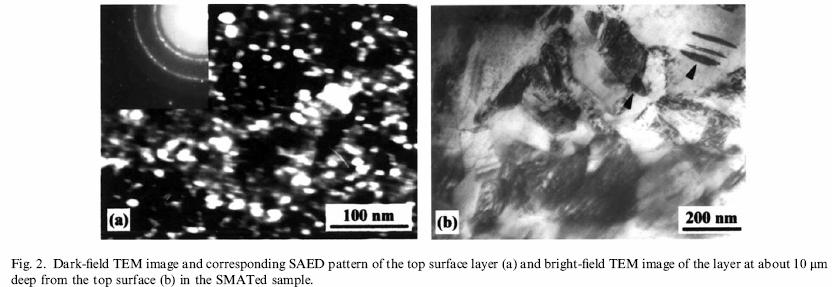
35 Friction and wear behaviors of nanocrystalline surface layer of pure copper Y.S. Zhang, Z. Han, K. Wang, K. Lu Wear 260 (2006) Surface mechanical attrition treatment (SMAT) was employed to fabricate a nanocrystalline surface layer on a pure copper plate. The grain size is about 10 nm in the top layer and increases with an increasing depth from the treated surface. 35

36 Selected area electron diffraction (SAED) 36
37 37
38 38

39 39

40 Effect of surface nanocrystallization on friction and wear properties in low carbon steel Z.B. Wang, N.R. Tao, S. Li b, W. Wang, G. Liu, J. Luc, K. Lu Materials Science and Engineering A352 (2003) 144/149 40
41 41
42 42
43 43

44 An abnormal strain rate effect on tensile behavior in nanocrystalline copper 44
45 45
46 原子力顯微鏡 AFM (Atomic Force Microscope) 46
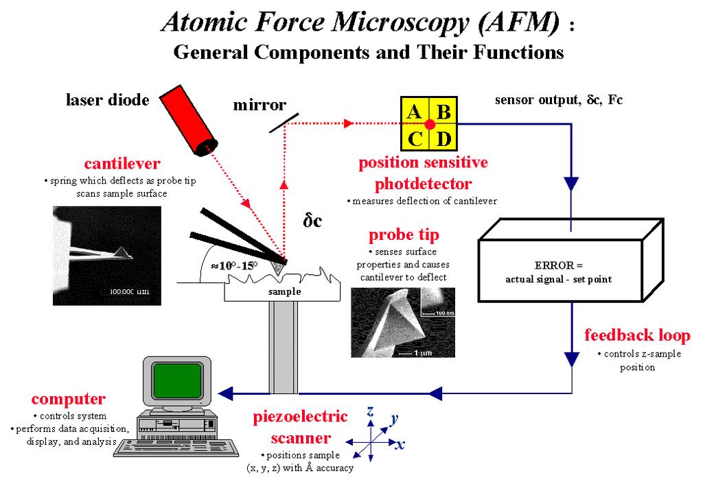
47 web.mit.edu/cortiz/www/nanomechanics.html AFM Tip 47
 Direct Effect( 直接效應 ) a well-known effect used in microphones, accelerometers etc. Converts mechanical strain into voltage.")
48 AFM 基本原理 探針與樣品表面的凡得瓦爾力 橫桿 (cantilever) 位移 200 µm with a low spring constant (of the order of 1 Newton/m) 雷射束偵測位移 掃瞄系統 迴饋電路系統 表面圖形 (surface topography) 高度影像 (height image) Piezo-electric Ceramics ( 壓電陶瓷 ) Direct Effect( 直接效應 ) a well-known effect used in microphones, accelerometers etc. Converts mechanical strain into voltage. Reverse Effect( 反相效應 ) a well-known effect used as a limited motion actuator, ultrasound transducer etc. Converts electrical fields into motion. 48
 up")
49 Record Player ( 唱片機 ) Z-axis is conventionally perpendicular to the sample. We may think that the AFM is like a record player Feedback Control Modes 迴授控制模式 With feedback control the positioning piezo which is moving the sample (or tip) up and down can respond to any changes in force constant force Without feedback control 49
50 AFM 操作模式 接觸式 (contact mode) 非接觸式 (non-contact mode) 輕敲式 (tapping mode) 接觸式 (Contact Mode) 排斥力 (repulsive) 最早發現 排斥力對距離敏感 解析度高 探針與樣品之作用力 10-6 ~10-10 N 作用力太大損害樣品 解析度 50
51 非接觸式 (Non-contact Mode) 解決接觸式 AFM 損害樣品之缺點 吸引力 ( 凡得瓦爾力 ) 對距離不敏感, 解析度不佳 改善解析度 探針需要與一陶瓷震盪片接觸 偵測振幅或相位 解析度 空氣中 :50nm ( 表面水模之影響 ) 真空 : 原子解析度 輕敲式 (Tapping Mode) 改良非接觸式 側向力減少 拉近探針與樣品距離 探針震盪至波谷時接觸樣品 共振頻率 (resonant frequency, hundreds of kilohertz) 較不受磨擦力之影響 樣品損害降低 硬質樣品損害探針 軟質物體受破壞 51
52 Tip Effects( 探針影響 ) One of the most important factors influencing the resolution Sharpness of the scanning tip The main influences are 寬度 (broadening) 與形狀比例 (aspect ratio) 壓縮 (compression) 交互作用力 (interaction forces) Tip Broadening( 探針寬度 ) Aspect Ratio ( 形狀比例 ) Radius of curvature of the tip Shape of the tip 52
53 Compression( 壓縮 ) Occurs when the tip is over the feature trying to be imaged. Difficult to determine in many cases how important this affect is. It should be born in mind that although the force between the tip and sample may only be nn, the pressure may be MPa. Interaction forces( 交互作用力 ) between the tip and sample The reason for image contrast with the AFM Forces due to the chemical nature of the tip are probably most important Selection of a particular tip for its material can be important 53


54 Specification of Cantilevers Length: 230 ± 5, µm Width: 40± 3, µm Thickness: 3.0 µm Resonant Frequency: 75 khz Force Constant: 3.5 N/m Images of Probe and Single Extratip Typical probe curvature radius : 1 nm Typical height of extratip: 100~200 nm 54


55 Tip Radius 1 nm curvature radius Scan size Height 250 nm 25 nm Conventional silicon probe in Tapping mode. Tip curvature radius Rc < 10 nm. Scan size Height 250 nm 40 nm HI'RES probe in Tapping mode. Individual molecules are resolved. Tip curvature radius Rc < 1 nm. 55
高溫黏度計 HIGH TEMPERATURE VISCOMETER
 高溫黏度計 HIGH TEMPERATURE VISCOMETER TA Instruments Bähr Products Rotating Viscometer VIS403 temperature range: max. 1500 C viscosity range: 1 10 7,5 dpas atmosphere: air, inert gas as purge gas Rotating
Gap Analysis for Drug Development Process
 Gap Analysis for Drug Process Dr. Jia Ming Chang AM4 Preclinical Animal Testing Center Institute for Drug Evaluation Platform Center for Biotechnology Benefit of Gap Analysis Gap analysis service support
CURRENT SENSING RESISTOR KRL SERIES- Susumu Co. Ltd. Thin Film Innovator
 CURRENT SENSING RESISTOR KRL SERIES- Susumu Co. Ltd. Thin Film Innovator OUTLINE -CURRENT SENSING RESISTOR KRL SERIES- 1 STRUCTURE 2 SEVERAL ADVANTAGES WITH COMPARISON DATA 3 APPLICATION MANUAL STRUCTURE
中港城 LED 廣告顯示屏收費 (A) LED 廣告顯示屏基本資料. 尺寸 : 1.6 米 ( 闊 ) x 4.8 米 ( 高 ) 每幅顯示屏 播放時間 :
 LED 廣告顯示屏基本資料. 尺寸 : 1.6 米 ( 闊 ) x 4.8 米 ( 高 ) 每幅顯示屏 播放時間 :") 中港城 LED 廣告顯示屏收費 (A) LED 廣告顯示屏基本資料 尺寸 : 1.6 米 ( 闊 ) x 4.8 米 ( 高 ) 每幅顯示屏 播放時間 : 星期一至日 : 早上九時至晚上九時 ( 播放時間如有更改, 恕不另行通知 ) 商戶廣告以每個月的第一天起開始計算 廣播時間 *: * 商戶可選擇以下之廣播時間及製訂廣告內容 ) 180 秒 / 每小時 (30 秒 / 視頻點 x 6/ 每小時或
中港城 LED 廣告顯示屏收費 (A) LED 廣告顯示屏基本資料 尺寸 : 1.6 米 ( 闊 ) x 4.8 米 ( 高 ) 每幅顯示屏 播放時間 : 星期一至日 : 早上九時至晚上九時 ( 播放時間如有更改, 恕不另行通知 ) 商戶廣告以每個月的第一天起開始計算 廣播時間 *: * 商戶可選擇以下之廣播時間及製訂廣告內容 ) 180 秒 / 每小時 (30 秒 / 視頻點 x 6/ 每小時或
Dwarfing peach trees and development of fruit quality by maintaining partially ringed bark strips as an innovative process in dwarfing technology
 Botanical Studies (2006) 47: 251-257. PHYSIOLOGY Dwarfing peach trees and development of fruit quality by maintaining partially ringed bark strips as an innovative process in dwarfing technology A.B.M.
FY06 ACCOMPLISHMENTS. Nanoelectronics Manufacture, Inspection, and Repair using Thermal Dip Pen Nanolithography
 FY06 ACCOMPLISHMENTS Nanoelectronics Manufacture, Inspection, and Repair using Thermal Dip Pen Nanolithography William P. King Georiga Institute of Technology FY06 was the second year of this grant, and
Cost Accounting class note : by Y. M. Hsieh 第九章材料之控制 成本計算與規劃
 第九章材料之控制 成本計算與規劃 一 材料取得與領用之會計處理 ( 一 ) 材料的採購 : 1. 生產性材料的採購 2. 物料 服務及維修的取得 :blanket purchase order 3. 採購用表單 :(1) 請購單 (Purchase Requisition) (2) 採購單 (Purchase Order) ( 二 ) 驗收 : 驗收報告 (Receiving Report) ( 三
頁數 (Page) 2 of 10 測試結果 (Test Results) 測試部位 (PART NAME)No.1 白色油墨 (WHITE INK) 鎘 / Cadmium (Cd) 鉛 / Lead (Pb) 汞 / Mercury (Hg) 測試項目 (Test Items) 六價鉻 / He
 2 of 10 測試結果 (Test Results) 測試部位 (PART NAME)No.1 白色油墨 (WHITE INK) 鎘 / Cadmium (Cd) 鉛 / Lead (Pb) 汞 / Mercury (Hg) 測試項目 (Test Items) 六價鉻 / He") 頁數 (Page) 1 of 10 以下測試樣品係由申請廠商所提供及確認 (The following sample(s) was/were submitted and identified by/on behalf of the applicant as) 送樣廠商 (Sample Submitted By) 樣品名稱 (Sample Description) 樣品型號 (Style/Item No.)
頁數 (Page) 1 of 10 以下測試樣品係由申請廠商所提供及確認 (The following sample(s) was/were submitted and identified by/on behalf of the applicant as) 送樣廠商 (Sample Submitted By) 樣品名稱 (Sample Description) 樣品型號 (Style/Item No.)
Clinical Management System from a Clinician prospective
 Clinical Management System from a Clinician prospective Dr CB Leung Consultant Department of Medicine and Therapeutics Prince of Wales Hospital Hospital Authority Convention 3 May 2016 1 Review epr Dx
Applied Biosystems StepOnePlus Real-time PCR System 之原理與應用介紹
 Applied Biosystems StepOnePlus Real-time PCR System 之原理與應用介紹 蔡如芸 (Judy Tsai, Ph.D.) Field Application Scientist The world leader in serving science Principle of Real-time PCR Normalised reporter fluorescence
Let our MyiQ on line! Bio-Rad Real-Time PCR Training Course. Pedro Lam 林華峰. Bio-Rad Laboratories 台灣分公司. Jan, 2008
 Let our MyiQ on line! Bio-Rad Real-Time PCR Training Course Pedro Lam 林華峰 Bio-Rad Laboratories 台灣分公司 Jan, 2008 Today Outline Part I: What is the Real-Time PCR? Part II: Software Training: Operation and
聚光型太陽電池發展趨勢 (OE_10290)
") 聚光型太陽電池發展趨勢 (OE_10290) 陳怡嘉 yjchen@mail.ndhu.edu.tw 國立東華大學光電工程學系 2015-03-27 (Friday) 14:10-17:00 (Contents are solely for educational purpose) 4. 聚光型太陽能電池 1. 組成系統 2. 電網等價 3. 聚光型太陽能電池分類 4. 電池模組結構說明 5. 電池模組結構分項說明
聚光型太陽電池發展趨勢 (OE_10290) 陳怡嘉 yjchen@mail.ndhu.edu.tw 國立東華大學光電工程學系 2015-03-27 (Friday) 14:10-17:00 (Contents are solely for educational purpose) 4. 聚光型太陽能電池 1. 組成系統 2. 電網等價 3. 聚光型太陽能電池分類 4. 電池模組結構說明 5. 電池模組結構分項說明
Recrystallization behavior of cold rolled Al Zn Mg Cu fabricated by twin roll casting
 Trans. Nonferrous Met. Soc. China 24(2014) 2226 2231 Recrystallization behavior of cold rolled Al Zn Mg Cu fabricated by twin roll casting Yun-Soo LEE, Won-Kyoung KIM, Dong-A JO, Cha-Yong LIM, Hyoung-Wook
商業智慧實務 Practices of Business Intelligence
 商業智慧實務 Practices of Business Intelligence Tamkang University 商業智慧導論 (Introduction to Business Intelligence) 1032BI01 MI4 Wed, 9,10 (16:10-18:00) (B130) Min-Yuh Day 戴敏育 Assistant Professor 專任助理教授 Dept.
In-Situ Monitoring of Pattern Filling in Nano-Imprint Lithography Using Surface Plasmon Resonance
 Copyright 2011 American Scientific Publishers All rights reserved Printed in the United States of America Journal of Nanoscience and Nanotechnology Vol. 11, 1 6, 2011 In-Situ Monitoring of Pattern Filling
Professor Chi-Wang Li, Ph.D.
 Professor Chi-Wang Li, Ph.D. Dept. of Water Resources & Environmental Engineering, TamKang University Tamsui 25137, Taipei, Taiwan Email: chiwang@mail.tku.edu.tw Office: (02) 2623-9343 Cell: 0968-585312
Leveraging the Precision of Electroforming over Alternative Processes When Developing Nano-scale Structures
 VOLUME 4 - ELECTROFORMING Leveraging the Precision of over Alternative Processes When Developing Nano-scale Structures Electrical and mechanical component and subsystem designers generally have five techniques
Advertising: The Art of Persuasion and Mirror to Society
 Advertising: The Art of Persuasion and Mirror to Society Grace Hsu Advertising is an effective marketing tool for reaching and informing consumers. However, it is not created in a vacuum; culture, economy,
Micro and nano structuring of carbon based materials for micro injection moulding and hot embossing
 Micro and nano structuring of carbon based materials for micro injection moulding and hot embossing Victor Usov, Graham Cross, Neal O Hara, Declan Scanlan, Sander Paulen, Chris de Ruijter, Daniel Vlasveld,
whether bar code or manual methods, depend on employees to record information, RFID relieves them from this time-consuming and error-prone process. Th
 The Application of the RFID and E-Seals in Container Shipping Yih-Ching Juang 莊義清 Department of Shipping and Transportation Management, National Penghu University of 摘要 Science and Technology 國立澎湖科技大學航運管理系
The Role of Silicone Surfactants as Surface Tension Reducing Agents in Polyurethane Foam
 The Role of licone Surfactants as Surface Tension Reducing Agents in Polyurethane Foam 硅油表面活性剂在聚氨酯发泡中所扮演的角色 Presented by: Masao Takase 高濑正男 Dow Corning Toray Co., Ltd. Translated by: KH Boo 巫光珂 Today s
奈米國家型科技計畫學術研究重要成果表 1. 計畫背景 :( 請以中 英文並呈 )
") 奈米國家型科技計畫學術研究重要成果表 填表日期 :95 年 5 月 16 日 1. 計畫背景 :( 請以中 英文並呈 ) 計畫主持人及執行機構 : 韋光華教授 (Principal Investigator: Professor Kung-Hwa Wei) 交通大學材料系 (Dept. of Materials Sci. & Eng., National Chiao Tung University)
奈米國家型科技計畫學術研究重要成果表 填表日期 :95 年 5 月 16 日 1. 計畫背景 :( 請以中 英文並呈 ) 計畫主持人及執行機構 : 韋光華教授 (Principal Investigator: Professor Kung-Hwa Wei) 交通大學材料系 (Dept. of Materials Sci. & Eng., National Chiao Tung University)
Mater. Res. Soc. Symp. Proc. Vol Materials Research Society
 Mater. Res. Soc. Symp. Proc. Vol. 940 2006 Materials Research Society 0940-P13-12 A Novel Fabrication Technique for Developing Metal Nanodroplet Arrays Christopher Edgar, Chad Johns, and M. Saif Islam
氮化硅陶瓷 Silicon Nitride Ceramics.
 氮化硅陶瓷 Silicon Nitride Ceramics www.visit-silicon.com Introduction The contents of nitrogen and silicon on the earth are very high. The content of nitrogen in the air is about 78.6%. Silicon is the element
HOW TO DEVELOP A SUCCESSFUL JOINT-VENTURE IN ASIA. is a business unit of
 HOW TO DEVELOP A SUCCESSFUL JOINT-VENTURE IN ASIA WHAT IS A JOINT-VENTURE SIMPLY PUT, A JOINT VENTURE (JV) IS NOTHING MORE THAN AN ECONOMIC COOPERATION, OR BUSINESS COMBINATION, OF TWO OR MORE PEOPLE,
Can Your Mobile Phone Smell? And How?
 National Cheng Kung University IBM: The 5 in 5, 2012 5 Innovations that will change our lives in the next five years Can Your Mobile Phone Smell? And How? 鄭桂忠副教授 (Kea-Tiong Tang, Ph.D) National Tsing Hua
Magnetic Force Microscopy: nanoscale magnetic imaging and lithography
 NTEGRA Aura Magnetic Force Microscopy: nanoscale magnetic imaging and lithography The principle of Magnetic Force Microscopy (MFM) is based on the detection of the interaction between the sample and a
MICROSTRUCTURAL INVESTIGATION OF SPD PROCESSED MATERIALS CASE STUDY
 TEQIP Workshop on HRXRD, IIT Kanpur, 05 Feb 2016 MICROSTRUCTURAL INVESTIGATION OF SPD PROCESSED MATERIALS CASE STUDY K.S. Suresh Department of Metallurgical and Materials Engineering Indian Institute of
THIN FILM THICKNESS MEASUREMENT FOR EVALUATION OF RESIDUAL LAYER OF NANO-IMPRINT LITHOGRAPHY USING NEAR-FIELD OPTICS
 9 th INTERNATIONAL SYMPOSIUM ON MEASUREMENT AND QUALITY CONTROL (9 th ISMQC) November 21 24, 27, IIT Madras THIN FILM THICKNESS MEASUREMENT FOR EVALUATION OF RESIDUAL LAYER OF NANO-IMPRINT LITHOGRAPHY
Micro-Electro-Mechanical Systems (MEMS) Fabrication. Special Process Modules for MEMS. Principle of Sensing and Actuation
 Fabrication. Special Process Modules for MEMS. Principle of Sensing and Actuation") Micro-Electro-Mechanical Systems (MEMS) Fabrication Fabrication Considerations Stress-Strain, Thin-film Stress, Stiction Special Process Modules for MEMS Bonding, Cavity Sealing, Deep RIE, Spatial forming
Micro-Electro-Mechanical Systems (MEMS) Fabrication Fabrication Considerations Stress-Strain, Thin-film Stress, Stiction Special Process Modules for MEMS Bonding, Cavity Sealing, Deep RIE, Spatial forming
Nanofabrication Prof. Stephen Y. Chou NanoStructure Laboratory
 Nanofabrication Prof. Stephen Y. Chou Department of Electrical Engineering Princeton University 1 Acknowledgment Dr. Paul Fischer Dr. Yun Wang Dr. Jay Guo Dr. Peter Klauss Dr. Jim Wang Dr. Longtin He Dr.
Microstructures and mechanical properties of pure magnesium bars by high ratio extrusion and its subsequent annealing treatment
 Trans. Nonferrous Met. Soc. China 22(2012) s445 s449 Microstructures and mechanical properties of pure magnesium bars by high ratio extrusion and its subsequent annealing treatment SUN Hong-fei 1,2, LI
PeakForce Tapping and ScanAsyst An introduction to the technique featuring Bruker s Dimension Edge. Bede Pittenger, Ph.D.
 PeakForce Tapping and ScanAsyst An introduction to the technique featuring Bruker s Dimension Edge Bede Pittenger, Ph.D. Dimension Edge with ScanAsyst: High performance AFM breaking down cost and productivity
Processing guidelines
 Processing guidelines mr-uvcur21 series UV-curable Polymer for UV-based Nanoimprint Lithography Characteristics mr-uvcur21 is a liquid UV-curable polymer system with low viscosity and high curing rate
YIELD & TENSILE STRENGTH OF STEEL & ALUMINIUM USING MICROINDENTATION
 YIELD & TENSILE STRENGTH OF STEEL & ALUMINIUM USING MICROINDENTATION Prepared by Duanjie Li, PhD & Pierre Leroux 6 Morgan, Ste156, Irvine CA 9618 P: 949.461.99 F: 949.461.93 nanovea.com Today's standard
Preparation and properties of porous silicon carbide ceramics through coat mix and composite additives process
 Preparation and properties of porous silicon carbide ceramics through coat mix and composite additives process ZHAO Hong sheng, LIU Zhong guo, YANG Yang, LIU Xiao xue, ZHANG Kai hong, LI Zi qiang Institute
Superionic Solid State Stamping (S4)
") Superionic Solid State Stamping (S4) Lead Faculty Researcher: Placid Ferreira Department: Materials Science & Engineering Hsu et al, Nano Letters, 2007 1. Description: This dry, single step, electrochemical
Superionic Solid State Stamping (S4) Lead Faculty Researcher: Placid Ferreira Department: Materials Science & Engineering Hsu et al, Nano Letters, 2007 1. Description: This dry, single step, electrochemical
Current Situation and Development Trend of Polycarboxylate Polyether (PCE) Macromonomer in China
 Macromonomer in China") Current Situation and Development Trend of Polycarboxylate Polyether (PCE) Macromonomer in China ZHU Jianmin Speaker: KONG Fanzhi Liaoning Oxiranchem Inc., P. R. China 2017.9.26, Munich Cotents 1. The
Current Situation and Development Trend of Polycarboxylate Polyether (PCE) Macromonomer in China ZHU Jianmin Speaker: KONG Fanzhi Liaoning Oxiranchem Inc., P. R. China 2017.9.26, Munich Cotents 1. The
Microstructure refinement by tool rotation-induced vibration in incremental sheet forming
 Available online at www.sciencedirect.com ScienceDirect Procedia Engineering 207 (2017) 795 800 International Conference on the Technology of Plasticity, ICTP 2017, 17-22 September 2017, Cambridge, United
Exploitation of AVRDC s Chili Pepper (Capsicum spp.) Germplasm in India 1
 Germplasm in India 1") 臺灣園藝 (J. Taiwan Soc. Hort. Sci.) 61(1):1-9, 2015 Exploitation of AVRDC s Chili Pepper (Capsicum spp.) Germplasm in India 1 亞蔬中心辣椒種原在印度的開發與利用 by M.K. Reddy 1, A. Srivastava 2, S.W. Lin 3, R. Kumar 4, H.C.
臺灣園藝 (J. Taiwan Soc. Hort. Sci.) 61(1):1-9, 2015 Exploitation of AVRDC s Chili Pepper (Capsicum spp.) Germplasm in India 1 亞蔬中心辣椒種原在印度的開發與利用 by M.K. Reddy 1, A. Srivastava 2, S.W. Lin 3, R. Kumar 4, H.C.
Towards scalable fabrication of high efficiency polymer solar cells
 Towards scalable fabrication of high efficiency polymer solar cells Hui Joon Park 2*, Myung-Gyu Kang 1**, Se Hyun Ahn 3, Moon Kyu Kang 1, and L. Jay Guo 1,2,3 1 Department of Electrical Engineering and
Metal extrusion. Metal stamping
 Metal extrusion Answer the following questions 1. In which of the following extrusion operation is friction a factor in determining the extrusion force (one best answer): (a) direct extrusion or (b) indirect
Effects of tribological behavior of DLC film on micro-deep drawing processes
 Trans. Nonferrous Met. Soc. China 24(2014) 2877 2882 Effects of tribological behavior of DLC film on micro-deep drawing processes Chun-ju WANG 1,2,3, Chuan-jie WANG 1,2, Bin GUO 1,2,3, De-bin SHAN 1,2,3
Precision Electroforming in High-Strength NiColoy
 Taking the Stress out of Electroforming www.nicoform.com Precision Electroforming in High-Strength NiColoy Copyright 2007 NiCoForm, Inc. (Rochester, NY) Electroforming What is it? What is it good for?
Delamination of Thin Films Using Laser Induced Stress Waves
 Center for Nanoscale Chemical-Electrical-Mechanical Manufacturing Systems Delamination of Thin Films Using Laser Induced Stress Waves Undergraduate Researcher Angelica Anne Vargas, Research Experience
STRENGTHENING MECHANISM IN METALS
 Background Knowledge Yield Strength STRENGTHENING MECHANISM IN METALS Metals yield when dislocations start to move (slip). Yield means permanently change shape. Slip Systems Slip plane: the plane on which
EXCIMER LASER ANNEALING FOR LOW- TEMPERATURE POLYSILICON THIN FILM TRANSISTOR FABRICATION ON PLASTIC SUBSTRATES
 EXCIMER LASER ANNEALING FOR LOW- TEMPERATURE POLYSILICON THIN FILM TRANSISTOR FABRICATION ON PLASTIC SUBSTRATES G. Fortunato, A. Pecora, L. Maiolo, M. Cuscunà, D. Simeone, A. Minotti, and L. Mariucci CNR-IMM,
Characterization of Two Chromogenic Media of Candida ID2 and CHROMagar Candida for Preliminary Identification of Yeasts
 Characterization of Two Chromogenic Media of Candida ID and for Preliminary Identification of Yeasts Chien-Fang Peng,, Kun-Mu Lee and Shuan-Hui Lee Laboratory of Microbiology and Clinical Microbiology,
Metallization deposition and etching. Material mainly taken from Campbell, UCCS
 Metallization deposition and etching Material mainly taken from Campbell, UCCS Application Metallization is back-end processing Metals used are aluminum and copper Mainly involves deposition and etching,
Cold Spray Developments at UTRC
 Hamilton Sundstrand Sikorsky Pratt & Whitney UTC Fire & Security Otis Elevator UTC Power Carrier Cold Spray Developments at UTRC Aaron Nardi United Technologies Research Center Cold Spray Action Team (CSAT)
Phases created during diffusion bonding of aluminium and aluminium bronze chips
 of Achievements in Materials and Manufacturing Engineering VOLUME 19 ISSUE 1 November 26 Phases created during diffusion bonding of aluminium and aluminium bronze chips J. Gronostajski, W. Chmura, Z. Gronostajski*
Poly-SiGe MEMS actuators for adaptive optics
 Poly-SiGe MEMS actuators for adaptive optics Blake C.-Y. Lin a,b, Tsu-Jae King a, and Richard S. Muller a,b a Department of Electrical Engineering and Computer Sciences, b Berkeley Sensor and Actuator
Interconnects. Outline. Interconnect scaling issues Aluminum technology Copper technology. Properties of Interconnect Materials
 Interconnects Outline Interconnect scaling issues Aluminum technology Copper technology 1 Properties of Interconnect Materials Metals Silicides Barriers Material Thin film Melting resistivity point ( C)
PARAMETER EFFECTS FOR THE GROWTH OF THIN POROUS ANODIC ALUMINUM OXIDES
 10.1149/1.2794473, The Electrochemical Society PARAMETER EFFECTS FOR THE GROWTH OF THIN POROUS ANODIC ALUMINUM OXIDES S. Yim a, C. Bonhôte b, J. Lille b, and T. Wu b a Dept. of Chem. and Mat. Engr., San
Texture evolution and its simulation of cold drawing copper wires produced by continuous casting
 Texture evolution and its simulation of cold drawing copper wires produced by continuous casting CHEN Jian 1, 2, YAN Wen 1, 2, LI Wei 3, MIAO Jian 4, FAN Xin-hui 2 1. Department of Applied Physics, Northwestern
Nanostructured electrochemical reactors for NOx/PM decomposition and micro SOFCs
 OECD Conference on Potential Environmental Benefits of Nanotechnology: Fostering Safe Innovation-Led Growth, Session 3. Clean Car Technology Paris, July 15-17, 2009 Nanostructured electrochemical reactors
Photolithography I ( Part 2 )
") 1 Photolithography I ( Part 2 ) Chapter 13 : Semiconductor Manufacturing Technology by M. Quirk & J. Serda Bjørn-Ove Fimland, Department of Electronics and Telecommunication, Norwegian University of Science
1 Photolithography I ( Part 2 ) Chapter 13 : Semiconductor Manufacturing Technology by M. Quirk & J. Serda Bjørn-Ove Fimland, Department of Electronics and Telecommunication, Norwegian University of Science
Choosing the Correct Capillary Design for Fine Pitch, BGA Bonding
 Choosing the Correct Capillary Design for Fine Pitch, BGA Bonding Lee Levine, Principal Engineer phone 215-784-6036, fax 215-784-6402, email: llevine@kns.com and Michael J. Sheaffer, Director Technical
Metal Forming Process. Prof.A.Chandrashekhar
 Metal Forming Process Prof.A.Chandrashekhar Introduction Shaping of a component by the application of external forces is known as the metal forming. Metal forming can be described as a process in which
CO2 hydrogenation to methanol over Cu/Zn/Al/Zr catalysts prepared by liquid reduction
 Chinese Journal of Catalysis 38 (2017) 717 725 催化学报 2017 年第 38 卷第 4 期 www.cjcatal.org available at www.sciencedirect.com journal homepage: www.elsevier.com/locate/chnjc Article CO2 hydrogenation to methanol
Lecture 5. SOI Micromachining. SOI MUMPs. SOI Micromachining. Silicon-on-Insulator Microstructures. Agenda:
 EEL6935 Advanced MEMS (Spring 2005) Instructor: Dr. Huikai Xie SOI Micromachining Agenda: SOI Micromachining SOI MUMPs Multi-level structures Lecture 5 Silicon-on-Insulator Microstructures Single-crystal
The most important parameters determining the performance of a cutting blade are:
 Diamond blades exceptionally wear resistant and extremely sharp P. Gluche 1, S. Strobel 1, H.-J. Fecht 2 1 GFD Gesellschaft für Diamantprodukte mbh, Lise-Meitner-Str. 13, 89081 Ulm, Germany 2 University
Esterification of cyclohexene with formic acid over a peanut shell derived carbon solid acid catalyst
 Chinese Journal of Catalysis 37 (216) 769 777 催化学报 216 年第 37 卷第 5 期 www.cjcatal.org available at www.sciencedirect.com journal homepage: www.elsevier.com/locate/chnjc Article Esterification of cyclohexene
Ecosystem Services and Cities: Case of Yokohama City and Kanagawa River Basin
 September 9 th, 2009 Urban Ecosystems and Biodiversity Ecosystem Services and Cities: Case of Yokohama City and Kanagawa River Basin Satoru Sadohara, Yokohama National University Outline The present state
The Current Condition and Development Trend of the Urban Water Supply and Drainage Facilities of China
 The Current Condition and Development Trend of the Urban Water Supply and Drainage Facilities of China 中国城市供水排水设施现状和发展趋势 Zhendong Li President of China Urban Water Association 中国城镇供水排水协会会长李振东 I. The current
Co-Evolution of Stress and Structure During Growth of Polycrystalline Thin Films
 Co-Evolution of Stress and Structure During Growth of Polycrystalline Thin Films Carl V. Thompson and Hang Z. Yu* Dept. of Materials Science and Engineering MIT, Cambridge, MA, USA Effects of intrinsic
NanoSteel 3rd Generation AHSS: Auto Evaluation and Technology Expansion
 NanoSteel 3rd Generation AHSS: Auto Evaluation and Technology Expansion Dr. D.J. Branagan Chief Technical Officer & Founder The NanoSteel Company Outline NanoSteel 3 rd Generation AHSS Structural formation
Microstructures and Mechanical Properties of Ultra Low Carbon IF Steel Processed by Accumulative Roll Bonding Process
 Materials Transactions, Vol. 43, No. 9 (22) pp. 232 to 2325 c 22 The Japan Institute of Metals EXPRESS REGULAR ARTICLE Microstructures and Mechanical Properties of Ultra Low Carbon IF Steel Processed by
KGC SCIENTIFIC Making of a Chip
 KGC SCIENTIFIC www.kgcscientific.com Making of a Chip FROM THE SAND TO THE PACKAGE, A DIAGRAM TO UNDERSTAND HOW CPU IS MADE? Sand CPU CHAIN ANALYSIS OF SEMICONDUCTOR Material for manufacturing process
Fracture of materials
 Fracture of materials Classification of fractureⅠ 1 Amount of plastic deformation Vertical fracture Cup and cone Type fracture Shear fracture (Separation of slip plane) Chisel point fracture Brittle fracture
Fabrication Techniques for Thin-Film Silicon Layer Transfer
 Fabrication Techniques for Thin-Film Silicon Layer Transfer S. L. Holl a, C. A. Colinge b, S. Song b, R. Varasala b, K. Hobart c, F. Kub c a Department of Mechanical Engineering, b Department of Electrical
Running head:celebrity ENDORSEING ADVERTISEMENT 1
 Running head:celebrity ENDORSEING ADVERTISEMENT 1 EVA Air s Brand Marketing and Jin, Cheng-Wu s Endorsing Advertisement Ya-Jing, Yang Class: UE4C Department of English Wenzao Ursuline University of Languages
Lecture 6. Through-Wafer Interconnect. Agenda: Through-wafer Interconnect Polymer MEMS. Through-Wafer Interconnect -1. Through-Wafer Interconnect -2
 Agenda: EEL6935 Advanced MEMS (Spring 2005) Instructor: Dr. Huikai Xie Lecture 6 Through-wafer Interconnect EEL6935 Advanced MEMS 2005 H. Xie 1/21/2005 1 Motivations: Wafer-level packaging CMOS 3D Integration
Cost effective manufacturing of tungsten heavy alloy foil and sheet material
 Manuscript refereed by Mr Dov Chaiat (Tungsten Powder Technology, Israel) Cost effective manufacturing of tungsten heavy alloy foil and sheet material D. Handtrack, B. Tabernig, H. Kestler, L.S. Sigl PLANSEE
Casting. Forming. Sheet metal processing. Powder- and Ceramics Processing. Plastics processing. Cutting. Joining.
 Traditional Manufacturing Processes Casting Forming Sheet metal processing Powder- and Ceramics Processing Plastics processing Cutting Joining Surface treatment FUNDAMENTALS OF METAL FORMING Overview of
Seismic Retrofit for a Network Arch Bridge with Slit-Type Knock-Off Bearings
 Seismic Retrofit for a Network Arch Bridge with -Type Knock-Off Bearings Koichi Sugioka Hanshin Expressway R&D Company Limited, Japan Nobuhiro Mashima Hanshin Expressway Company Limited, Japan Hiroaki
RESIDUAL STRESS REDUCTION IN HIGH PRESSURE INTERPASS ROLLED WIRE+ARC ADDITIVE MANUFACTURING TI-6AL-4V COMPONENTS
 RESIDUAL STRESS REDUCTION IN HIGH PRESSURE INTERPASS ROLLED WIRE+ARC ADDITIVE MANUFACTURING TI-6AL-4V COMPONENTS Filomeno Martina a,, Matthew Roy b, Paul Colegrove a, Stewart W. Williams a a Welding Engineering
Uncrosslinked SU-8 as a sacrificial material
 INSTITUTE OFPHYSICS PUBLISHING JOURNAL OF MICROMECHANICS AND MICROENGINEERING J. Micromech. Microeng. 15 (2005) N1 N5 doi:10.1088/0960-1317/15/1/n01 TECHNICAL NOTE Uncrosslinked as a sacrificial material
Managing Climate Change Effect on Groundwater through Monitoring Groundwater. 16 October 2011 People s Republic of China Gao Zhanyi
 Managing Climate Change Effect on Groundwater through Monitoring Groundwater Group Field Science& Technology Strategy 16 October 2011 People s Republic of China Gao Zhanyi 1 Implementing Organization Operating
LOW TEMPERATURE PHOTONIC SINTERING FOR PRINTED ELECTRONICS. Dr. Saad Ahmed XENON Corporation November 19, 2015
 LOW TEMPERATURE PHOTONIC SINTERING FOR PRINTED ELECTRONICS Dr. Saad Ahmed XENON Corporation November 19, 2015 Topics Introduction to Pulsed Light Photonic sintering for Printed Electronics R&D Tools for
Model 629A31. Precision Triaxial Industrial ICP Accelerometer. Installation and Operating Manual
 Model 629A31 Precision Triaxial Industrial ICP Accelerometer Installation and Operating Manual For assistance with the operation of this product, contact PCB Piezotronics, Inc. Toll-free: 800-959-4464
A Technical Study of the Double-ram Zun Ancient Chinese Bronze Vessel in the British Museum
 Radiance between Bronze and Jade Archaeology, Art, and Culture of the Shang and Zhou Dynasties Taipei Institute of History and Philology, Academia Sinica Published date November 2013 Page 257-283 A Technical
Lecture 19 Microfabrication 4/1/03 Prof. Andy Neureuther
 EECS 40 Spring 2003 Lecture 19 Microfabrication 4/1/03 Prof. ndy Neureuther How are Integrated Circuits made? Silicon wafers Oxide formation by growth or deposition Other films Pattern transfer by lithography
Mechanism of debismuthizing with calcium and magnesium
 Trans. Nonferrous Met. Soc. China 23(2013) 1501 1505 Mechanism of debismuthizing with calcium and magnesium Dian-kun LU, Zhe-nan JIN, Yong-feng CHANG, Shu-chen SUN School of Materials and Metallurgy, Northeastern
Utilization of nickel slag using selective reduction followed by magnetic separation
 Trans. Nonferrous Met. Soc. China 23(2013) 3421 3427 Utilization of nickel slag using selective reduction followed by magnetic separation Jian PAN, Guo-lin ZHENG, De-qing ZHU, Xian-lin ZHOU School of Minerals
Microcontact Printing Procedures for Adhesive and Conductive Epoxies
 Microcontact Printing Procedures for Adhesive and Conductive Epoxies This objective was accomplished through a formal record of the procedures to deliver a stamped product which met the benchmark mechanical,
Request for 4M change self management strengthening
 Request for 4M change self management strengthening 1.Aug.2016 Device engineering Dep. Partner management Dep. Sony Global M&O Corp. 1 Request for 4M change self management strengthening Past cases of
Recrystallization Theoretical & Practical Aspects
 Theoretical & Practical Aspects 27-301, Microstructure & Properties I Fall 2006 Supplemental Lecture A.D. Rollett, M. De Graef Materials Science & Engineering Carnegie Mellon University 1 Objectives The
Forming limit of textured AZ31B magnesium alloy sheet at different temperatures
 Forming limit of textured AZ31B magnesium alloy sheet at different temperatures HUANG Guang-sheng 1, 2, ZHANG Hua 1, 2, GAO Xiao-yun 1, SONG Bo 1, 2, ZHANG Lei 1, 2 1. College of Materials Science and
Model 106B. ICP Pressure Sensor. Installation and Operating Manual
 Model 106B ICP Pressure Sensor Installation and Operating Manual For assistance with the operation of this product, contact PCB Piezotronics, Inc. Toll-free: 800-828-8840 24-hour SensorLine: 716-684-0001
Photonic Drying Pulsed Light as a low Temperature Sintering Process
 Photonic Drying Pulsed Light as a low Temperature Sintering Process Lou Panico Xenon Corporation W E S T E R N M I C H I G A N U N I V E R S I T Y PRESENTATION OVERVIEW What is Printed Electronics Materials
Introduction to Engineering Materials ENGR2000 Chapter 8: Failure. Dr. Coates
 Introduction to Engineering Materials ENGR2000 Chapter 8: Failure Dr. Coates Canopy fracture related to corrosion of the Al alloy used as a skin material. 8.2 Fundamentals of Fracture Fracture is the separation
Influence of deformation passes on interface of SiC p /Al composites consolidated by equal channel angular pressing and torsion
 Trans. Nonferrous Met. Soc. China 25(2015) 1376 1382 Influence of deformation passes on interface of SiC p /Al composites consolidated by equal channel angular pressing and torsion Chen-hao QIAN, Ping
Model 646B ma Output Accelerometer. Installation and Operating Manual
 Model 646B00 4-20 ma Output Accelerometer Installation and Operating Manual For assistance with the operation of this product, contact PCB Piezotronics, Inc. Toll-free: 800-959-4464 24-hour SensorLine:
Surface Characterization of Laser Polished Indirect-SLS Parts
 Surface Characterization of Laser Polished Indirect-SLS Parts Jorge A. Ramos, David L. Bourell, Joseph J. Beaman Laboratory for Freeform Fabrication The University of Texas at Austin, Austin, Texas 78712
Showerhead amenities for reduced energy use and standardization of hot water conservation
 Showerhead amenities for reduced energy use and standardization of hot water conservation Masayuki Mae Associate Professor, The University of Tokyo Akinori Suzuki Tokyo Gas Company, Ltd. Yuhi Murakami
MICROFABRICATION OF OPTICALLY ACTIVE InO X MICROSTRUCTURES BY ULTRASHORT LASER PULSES
 Journal of Optoelectronics and Advanced Materials Vol. 4, No. 3, September 2002, p. 809-812 MICROFABRICATION OF OPTICALLY ACTIVE InO X MICROSTRUCTURES BY ULTRASHORT LASER PULSES Foundation for Research
Effect of particle size distribution on properties of zirconia ceramic mould for TiAl investment casting
 Effect of particle size distribution on properties of zirconia ceramic mould for TiAl investment casting CHEN Yan-fei, XIAO Shu-long, TIAN Jing, XU Li-juan, CHEN Yu-yong School of Materials Science and