Insulated Metal Substrates
|
|
|
- Roberta Johnston
- 6 years ago
- Views:
Transcription
1 Insulated Metal Substrates Presented by Les Round of Spirit Circuits ICT Evening Seminar: 15 th September 2010 Venue: Newtown Hotel, Hayling Island
2 Why use Thermal Management The failure rate of an electronic device doubles with every 10C increase in chip junction temperature. (Source: AI Technology) So it pays to keep it cool.
3 Growth in demand for Metal-back PCB s LED Lighting provides energy efficient, low maintenance & long-life lighting solutions. Power Solutions power conversion, distribution, charging and storage systems (aided by new generating technology wind, solar power etc). Electric Cars PCB s associated with actual vehicles and potential from a network of charging points. LCD TV LED back-lighting.
4 Typical Metal-back Substrate Circuit Copper Dielectric Layer Metal Base
5 What are Metal-back Substrates Copper foil track & pad layer. (1 10oz). Dielectric layer electrical insulation (500-1kV/25micron) - thermally conductive (1 8W/mK) - thickness ( mm) Metal Base heat sink. ( mm) - aluminium (150W/mK) - copper (400W/mK)
6 IMS SELECTION CITERIA Electrical performance Thermal requirements Metal base Cost
7 Electrical Performance Copper cladding: - select copper weight based on required current carrying capacity and thermal needs. Electrical isolation: - select based on breakdown voltage (0.5 1kV/mil) versus dielectric thickness.
8 Thermal Requirements Thermal Impedance of an IMS indicates how effective heat is removed from a component lower the thermal impedance the more efficient heat is dissipated. In practice, the selection is based on the dielectric thickness versus the Thermal Conductivity.
9 Metal Base Aluminium is; typically; the default material because of cost & weight. Copper selected where: - CTE may be an issue (heavy copper) - electrical contact to the base may be required (especially via a PTH) - better thermal conductivity required
10 Cost Cost is a key factor in the choice of an IMS material because; especially in the LED arena; a low unit price is critical. Therefore, selection is usually based on the lowest cost option in order to achieve the required overall performance.
11 Comparison or IMS v FR4 for a given design (Temp. rise 10 C/3oz Copper tracks) 40 Track Width (mm) mm, 2.2W/MK IMS 1.6mm, FR Current (Amps)
12 IMS Suppliers Aismalibar ( AI Technology ( Arlon ( Bergquist ( Denka ( ( DuPont ( Laird ( Taconic ( Thermastrate ( Ventec (
13 Manufacturing 1. Engineering and tooling 2. Imaging 3. Etch 4. Inspect 5. Solder Resist and Ident 6. Solderable Finish 7. Profile 8. Final Test and Inspection
14 Engineering & Tooling Flexible tooling system preferred for optimum panel utilisation. Provide feedback to customer about panelisation (where possible, design around 18x24inch panel). Drill or punch tooling holes into panels.
15 Imaging Produce etch resist image using photoresist or etch-resist inks.
16 Etch Mask-off the metal base with either photoresist or etch-resist ink; or, buy-in IMS with a polyester protective film applied to metal base. Etch with either alkaline or acid etchant.
17 Inspect AOI is a useful tool especially where no final test is required.
18 Solder Resist & Ident Solder resist is applied either by standard screenprint or photoimageable process. White resist is commonly specified for LED applications and there are a range of bespoke resist available that are colour stable (through assembly and in use). Ident is applied using standard screenprint process but photoimageable or jet-print used for high copper weights.
19 Solderable Finish All popular finishes are used (including special finishes for gold wire bonding). ENIG used for aluminium wire bonding applications and for use with copper based materials. OSP & LF HASL most common for LED market.
20 Profile Routing used for smaller volume production using fluted cutters. Scoring common for square or rectangular boards using diamond or zirconium nitride tipped blades. Blanking for high volumes using hardened steel or tungsten carbide tools.
21 Test Standard electrical test. Flash test batch test (typically 1KV) or bespoke testing (up to 5KV).
22 Thermal Tapes Basically a thermally conductive, electrically insulating, double-sided tape used for screwless fixing and aides heat dissipation. Simple application but need to ensure no air is trapped between tape & heat sink. Profile needs to be optimised to ensure the tape is cut cleanly.
23 Non-Standard IMS boards Example 1: 4oz, PTH or multilayer PCB using Laird material bonded to a 2mm metal base (copper or aluminium) with Laird TPreg. Base is machined with rebates, countersink & counterbore holes. Some versions have the PCB connected to the base using plated through holes. ENIG finish to circuit side & copper bases with anodising for the aluminium bases.
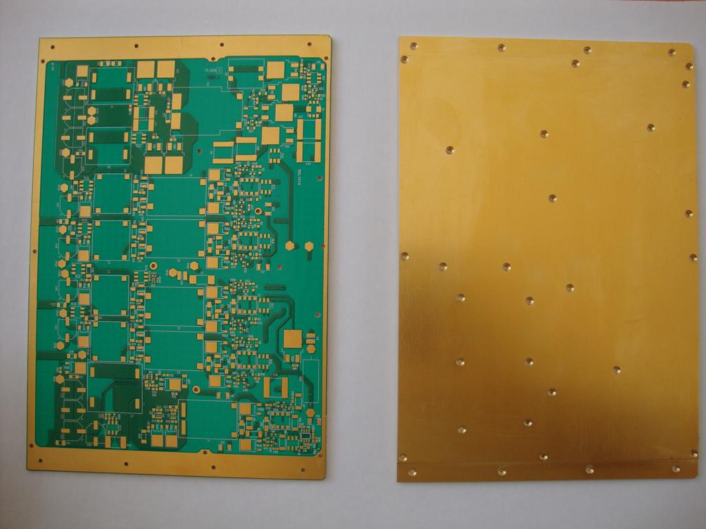
24 Example 1
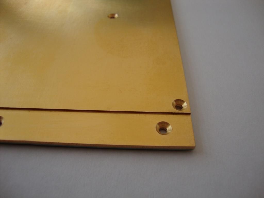
25 Example 1
26 Non-Standard IMS boards Example 2. Customer requirement was for an IMS circuit to be supplied in an array for mass assembly and then the circuit would be broken-out of the array and specific areas of the board would be bent through 90 degrees without affecting the integrity of the circuit. Solution: trials were carried-out by bonding custom-made materials; after a successful evaluation by the customer, the job went into production. Ventec now supply a similar material which is used for all production requirements.
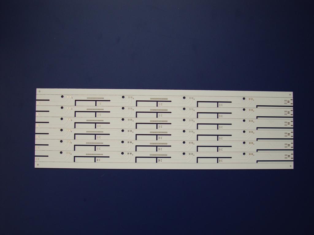
27 Example 2
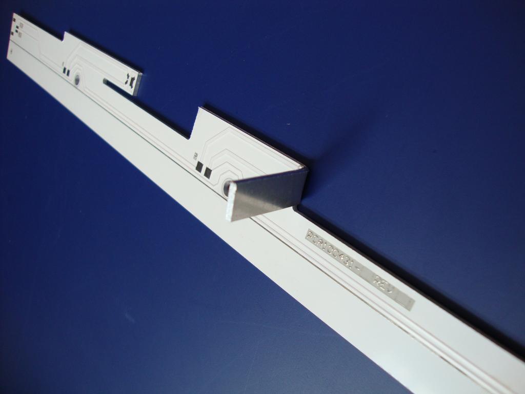
28 Example 2
29 Non-Standard IMS boards Example 3. 5oz, 0.1mm FR4 PTH board bonded to a pre-machined 1.00mm copper base. Finish is immersion silver.
30 Example 3
PCB Production Process HOW TO PRODUCE A PRINTED CIRCUIT BOARD
 NCAB Group Seminars PCB Production Process HOW TO PRODUCE A PRINTED CIRCUIT BOARD NCAB GROUP PCB Production Process Introduction to Multilayer PCBs 2 Introduction to multilayer PCB s What is a multilayer
COFAN USA. Meeting your Project needs.
 COFAN USA Meeting your Project needs www.cofangroup.com PCB Substrate Pre-preg Category SEKISUI Laird T-Clad Denka PCB Substrate Pre-preg Category In the PCB industry, there are a couple major Pre-preg
GRAPHIC MANUFACTURING CAPABILITY Q217-18
 All features are design dependent and may not be achievable in combination Reduced Yield / Special values up ( or down ) to the standard limit are design and application dependent Standard features only
c/bach, 2-B Pol. Ind Foinvasa Montcada i Reixac (Barcelona) SPAIN Tel FAX
 SPAIN Tel FAX") 1- What is 2- How does it work? 3- How do we make it? 4- Applications 5- Processing? WHAT IS? Thick aluminium based substrate, cladded in ED copper foil. Designed for an effective thermal dissipation and
1- What is 2- How does it work? 3- How do we make it? 4- Applications 5- Processing? WHAT IS? Thick aluminium based substrate, cladded in ED copper foil. Designed for an effective thermal dissipation and
Optimizing the Insulated Metal Substrate Application with Proper Material Selection and Circuit Fabrication
 Abstract Optimizing the Insulated Metal Substrate Application with Proper Material Selection and Circuit Fabrication Dave Sommervold, Chris Parker, Steve Taylor, Garry Wexler. The Bergquist Company Prescott,
Introduction Conductors. Supply Planes. Dielectric. Vias PCB Manufacturing Process Electronic Assembly Manufacturing Process
 PCBs/Overview Printed Circuit Boards (PCB) Introduction Conductors. Supply Planes. Dielectric. Vias PCB Manufacturing Process Electronic Assembly Manufacturing Process 29/09/2005 EE6471 (KR) 263 PCBs/Overview
Qualification and Performance Specification for Flexible Printed Boards
 Qualification and Performance Specification for Flexible Printed Boards Developed by the Flexible Circuits Performance Specifications Subcommittee (D-12) of the Flexible Circuits Committee (D-10) of IPC
PCB Technologies for LED Applications Application note
 PCB Technologies for LED Applications Application note Abstract This application note provides a general survey of the various available Printed Circuit Board (PCB) technologies for use in LED applications.
Low CTE / High Tg FR-4 with High Heat Resistance
 Low CTE / High Tg FR-4 with High Heat Resistance Laminate: EM-827 Prepreg: EM-827B 1 Features Tg(DSC) > 170 Z direction CTE < 3.0% (50~260 ) High thermal degradation temperature: Td > 340 Excellent thermal
Flexible Printed Circuits Design Guide
 www.tech-etch.com/flex Flexible Printed Circuits Design Guide Multilayer SMT Assembly Selective Plating of Gold & Tin-Lead Fine Line Microvias Cantilevered & Windowed Leads 1 MATERIALS CONDUCTOR Copper
!"#$#%&#'(() ) **+,-./01)2-,-.3)456,1) /0! **)
 ) **+,-./01)2-,-.3)456,1) /0! **)") !"#$#%&#'(() ) **+,-./01)2-,-.3)456,1) /0!7.5853-09**) Etching Removal of unwanted or non-circuit copper from board Etch resists organic and metallic resists photoresist tin, gold, nickel, silver and alloys
!"#$#%&#'(() ) **+,-./01)2-,-.3)456,1) /0!7.5853-09**) Etching Removal of unwanted or non-circuit copper from board Etch resists organic and metallic resists photoresist tin, gold, nickel, silver and alloys
FLEXIBLE & RIGID-FLEX CIRCUITS TECHNICAL ENGINEERING GUIDE. Delivering Quality Since 1952.
 FLEXIBLE & RIGID-FLEX CIRCUITS TECHNICAL ENGINEERING GUIDE Delivering Quality Since 1952. DELIVERING QUALITY SINCE 1952. Epec Engineered Technologies designs and manufactures customized, built-to-print,
RF-43. General Processing Guidelines
 RF-43 General Processing Guidelines Petersburgh, NY Tel: 800-833-1805 Fax: 518-658-3988 Europe Tel: +353-44-38300 Fax: +353-44-44369 Asia Tel: +82-31-704-1858 Fax: +82-31-704-1857 www.taconic-add.com www.taconic.co.kr
Reliability of Interconnects in LED Lighting Assemblies Utilizing Metal Clad Printed Circuit Boards Stefano Sciolè BDM I.M.S.
 Reliability of Interconnects in LED Lighting Assemblies Utilizing Metal Clad Printed Circuit Boards Stefano Sciolè BDM I.M.S. Henkel Electronic Materials Agenda 1. Introduction 2. Motivation 3. Interconnect
High Efficiency UV LEDs Enabled by Next Generation Substrates. Whitepaper
 High Efficiency UV LEDs Enabled by Next Generation Substrates Whitepaper Introduction A primary industrial market for high power ultra-violet (UV) LED modules is curing equipment used for drying paints,
Nontraditional Machining Processes
 Nontraditional Machining Processes The NTM processes can be divided into four basic categories: I. Chemical (Chemical reaction), II. Electrochemical (Electrolytic dissolution), III. Mechanical (Multipoint
IMPACT OF MICROVIA-IN-PAD DESIGN ON VOID FORMATION
 IMPACT OF MICROVIA-IN-PAD DESIGN ON VOID FORMATION Frank Grano, Felix Bruno Huntsville, AL Dana Korf, Eamon O Keeffe San Jose, CA Cheryl Kelley Salem, NH Joint Paper by Sanmina-SCI Corporation EMS, GTS
TECHNICAL DATA SHEET 1 P a g e Revised January 9, 2014
 1 P age Revised January 9, 2014 TAIYO PSR-4000 CC01SE (UL Name: PSR-4000JV / CA-40JV) LIQUID PHOTOIMAGEABLE CURTAIN COAT SOLDER MASK Curtain Coat Application Aqueous Developing Solder Mask RoHS Compliant
NCAB Group PCB Specification
 NCAB Group Seminar no. 9 NCAB Group PCB Specification NCAB GROUP NCAB Group PCB Specification 14 key features for durable and reliable PCB s NCAB GROUP NCAB Group PCB Specification 2 Are all PCB s created
Bright Lights, Big Finish
 Reprinted From: Products Finishing Magazine Bright Lights, Big Finish for Electronics Plater Wisconsin maker of PCB for the LED industry adds new finishing line. BY TIM PENNINGTON EDITOR Business of late
Keeping Cool!: selecting high performance thermal materials for LED Lighting applications. Ian Loader 25/03/14
 Keeping Cool!: selecting high performance thermal materials for LED Lighting applications Ian Loader 25/03/14 1 Target Points to cover Basics of Thermal Management Considerations for thermal materials
A STUDY OF THE ENEPIG IMC FOR EUTECTIC AND LF SOLDERS
 A STUDY OF THE ENEPIG IMC FOR EUTECTIC AND LF SOLDERS G.Milad, D.Gudeczauskas, G.Obrien, A.Gruenwald Uyemura International Corporation Southington, CT ABSTRACT: The solder joint formed on an ENEPIG surface
Process & Capability Manual (Vol )
") Process & Capability Manual (Vol. 12-2015) Seite 1 von 13 1 CHAPTER OVERVIEW 1 CHAPTER OVERVIEW... 2 2 MICROCIRTEC A SHORT PROFILE... 3 2.1 WHO WE ARE... 3 2.2 OBJECTIVES & MARKETS... 3 2.3 DECLARATION
Process & Capability Manual (Vol. 12-2015) Seite 1 von 13 1 CHAPTER OVERVIEW 1 CHAPTER OVERVIEW... 2 2 MICROCIRTEC A SHORT PROFILE... 3 2.1 WHO WE ARE... 3 2.2 OBJECTIVES & MARKETS... 3 2.3 DECLARATION
High Frequency Circuit Materials Attributes John Coonrod, Rogers Corporation
 High Frequency Circuit Materials Attributes John Coonrod, Rogers Corporation Specialty high frequency circuit materials have been used in the PCB industry for decades and for many different reasons. There
MCPCB Material (Heat sync)
") MCPCB Material (Heat sync) NIPPON RIKA KOGYOSHO CO.,LTD Feb Metal Base CCL (Heat sync) Metal Base CCL (Heat sync) Copper Foil FR-4 High Performance Epoxy Metal Base Glass Cloth + Epoxy Etching Etching
MCPCB Material (Heat sync) NIPPON RIKA KOGYOSHO CO.,LTD Feb Metal Base CCL (Heat sync) Metal Base CCL (Heat sync) Copper Foil FR-4 High Performance Epoxy Metal Base Glass Cloth + Epoxy Etching Etching
PEC (Printed Electronic Circuit) process for LED interconnection
 process for LED interconnection") PEC (Printed Electronic Circuit) process for LED interconnection Higher wattage LED s/ power components or their placement in higher densities, requires a larger dissipation of heat in a more effective
PEC (Printed Electronic Circuit) process for LED interconnection Higher wattage LED s/ power components or their placement in higher densities, requires a larger dissipation of heat in a more effective
Precision Engineered Parts
 Precision Engineered Parts Photoetching Laser Cutting Forming Finishing Thin Metal Parts Flexible Circuits EMI Shielding Gaskets www.tech-etch.com PHOTOETCHING Tech-Etch specializes in the manufacture
curamik CERAMIC SUBSTRATES AMB technology Design Rules Version #04 (09/2015)
") curamik CERAMIC SUBSTRATES AMB technology Design Rules Version #04 (09/2015) Content 1. Geometric properties 1.01. Available ceramic types / thicknesses... 03 1.02. thicknesses (standard)... 03 3. Quality
curamik CERAMIC SUBSTRATES AMB technology Design Rules Version #04 (09/2015) Content 1. Geometric properties 1.01. Available ceramic types / thicknesses... 03 1.02. thicknesses (standard)... 03 3. Quality
UL PCB Recognition what is it & why do you need to know about it
 UL PCB Recognition what is it & why do you need to know about it Presented by Emma Hudson NCAB Customer Event March 2015 UL and the UL logo are trademarks of UL LLC 2015 Agenda What is UL and what are
Carbon film resistors
 Carbon film resistors (6.3 φ 2.4 size: 1 / 3W) ROHM resistors are produced using an integrated production system for parts and materials, and state of the art technology to ensure high precision productivity,
Surface Mount Sense Resistors
 Resistors Surface Mount Flexible leads for thermal expansion Open-air design reduces PCB heating Values down to 1milliohm Element TCR ±2ppm/ C Zero-ohm 65A jumper version RoHS compliant All parts are Pb-free
MICROWAVE & RF MATERIALS GUIDE
 MICROWAVE & RF MATERIALS GUIDE RF & Microwave Materials Guide Arlon Microwave Materials specializes in products made from fluoropolymers (i.e. PTFE), ceramic-filled fluoropolymers, ceramic-filled hydrocarbon
VTT TECHNICAL RESEARCH CENTRE OF FINLAND. LTCC Packaging & Smart System Integration Horten Kari Kautio
 LTCC Packaging & Smart System Integration Horten 19.9.2008 Kari Kautio 1 OUTLINE LTCC technology - processing and materials Thermal management Bare die assembly & sealing Application areas & demonstrators
How to select PCB materials for highfrequency
 How to select PCB materials for highfrequency apps Find out how to simplify that choice when striving for the best tradeoff between ease of fabrication and best electrical performance. By John Coonrod
Offshore Wind Turbines Power Electronics Design and Reliability Research
 Offshore Wind Turbines Power Electronics Design and Reliability Research F. P. McCluskey CALCE/Dept. Of Mechanical Engineering University of Maryland, College Park, MD (301) 405-0279 mcclupa@umd.edu 1
Flex and Rigid-Flex Printed Circuit Design
 Flex and Rigid-Flex Printed Circuit Design Old Content - visit altium.com/documentation Modified by on 29-Nov-2016 Related Videos Bending Lines Enhanced Layer Stack Management Layer Stack Regions A rigid-flex
ESPANEX L Series. Technical data sheet Nishigotanda Shinagawa Tokyo, , Japan TEL FAX
 ESPANEX L Series Technical data sheet This sheet will be changed without any information in advance. The data on this sheet are solely for your reference and are not to be constructed as constituting a
HBLED packaging is becoming one of the new, high
 Ag plating in HBLED packaging improves reflectivity and lowers costs JONATHAN HARRIS, President, CMC Laboratories, Inc., Tempe, AZ Various types of Ag plating technology along with the advantages and limitations
Lead Free Assembly: A Practical Tool For Laminate Materials Selection
 Lead Free Assembly: A Practical Tool For Laminate Materials Selection Erik J. Bergum David Humby Isola Abstract: The impending European RoHS legislation, restricting the use of lead containing solders,
Soldermasks - Processes and Properties
 Soldermasks - Processes and Properties Soldermask what is it for Enable mass soldering techniques Prevent solder shorts under components Prevent corrosion to underlying circuitry Plating resist for surface
Etching. quick clean burr-free
 Etching quick clean burr-free higher quality. Lower costs. Ä t z t e c h n i k h e r z / / B e n e f i t S 03 keeping an eye on costs doesn t mean you have to cut corners on quality. reduce your costs
Power Electronics Packaging Solutions for Device Junction Temperature over 220 o C
 EPRC 12 Project Proposal Power Electronics Packaging Solutions for Device Junction Temperature over 220 o C 15 th August 2012 Page 1 Motivation Increased requirements of high power semiconductor device
3M Thermally Conductive Adhesive Tape 8940
 Product Information Sheet 15. Oct 2004 Supersedes Version 01. Mai 2004 Product Description 3M TM Thermally Conductive Adhesive Tape 8940 is designed to provide an efficient heat transfer path between heat
1/2W, 0805 Low Resistance Chip Resistor (Lead / Halogen free)
") 1. Scope 1/2W, 0805 (Lead / Halogen free) This specification applies to 1.2mm x 2.0mm size 1/2W, fixed metal film chip resistors rectangular type for use in electronic equipment. 2. Type Designation RL
1. Scope 1/2W, 0805 (Lead / Halogen free) This specification applies to 1.2mm x 2.0mm size 1/2W, fixed metal film chip resistors rectangular type for use in electronic equipment. 2. Type Designation RL
Embedding Passive and Active Components: PCB Design and Fabrication Process Variations
 Embedding Passive and Active Components: PCB Design and Fabrication Process Variations Vern Solberg Solberg Technical Consulting Saratoga, California USA Abstract Embedding components within the PC board
3 Thermally Conductive Tapes
 3 Thermally Conductive Tapes Technical Data July, 21 Product Description 3M Thermally Conductive Tapes 885, 881, and 8815 are designed to provide a preferential heat-transfer path between heat-generating
KGC SCIENTIFIC Making of a Chip
 KGC SCIENTIFIC www.kgcscientific.com Making of a Chip FROM THE SAND TO THE PACKAGE, A DIAGRAM TO UNDERSTAND HOW CPU IS MADE? Sand CPU CHAIN ANALYSIS OF SEMICONDUCTOR Material for manufacturing process
10 Manor Parkway, Suite C Salem, New Hampshire
 Micro-Precision Technologies (MPT) is an independent manufacturer of hybrid integrated circuits, multichip modules, and high-precision thick film substrates for the military, medical, avionics, optoelectronics,
A Solder Joint Reliability Model for the Philips Lumileds LUXEON Rebel LED Carrier Using Physics of Failure Methodology
 A Solder Joint Reliability Model for the Philips Lumileds LUXEON Rebel LED Carrier Using Physics of Failure Methodology Rudi Hechfellner 1, Michiel Kruger 1, Tewe Heemstra 2 Greg Caswell 3, Nathan Blattau
Packaging Technologies for SiC Power Modules
 Packaging Technologies for SiC Power Modules Masafumi Horio Yuji Iizuka Yoshinari Ikeda ABSTRACT Wide bandgap materials such as silicon carbide (SiC) and gallium nitride (GaN) are attracting attention
ELECTRONIC MANUFACTURING SERVICES
 ELECTRONIC MANUFACTURING SERVICES 2017 THICK FILM ON ALUMINA THICK FILM ON ALUMINIUM NITRIDE THICK FILM ON ALUMINUM SMT MANUFACTURING SERVICE INSULATE METAL SUBSTRATE POWER RESISTORS ON STAINLESS STEEL
DIBOND 3A COMPOSITES. The ultimate aluminum composite Material (Acm) Sales Training Presentation by 3A Composites Level 201
 Sales Training Presentation by 3A Composites Level 201") DIBOND The ultimate aluminum composite Material (Acm) Sales Training Presentation by 3A Composites Level 201 2 0 10 USA, INC. Introduction Welcome to the Sales Training Presentation by 3A Composites In
DIBOND The ultimate aluminum composite Material (Acm) Sales Training Presentation by 3A Composites Level 201 2 0 10 USA, INC. Introduction Welcome to the Sales Training Presentation by 3A Composites In
High Temperature (245 C) Thick Film Chip Resistor
 Thick Film Chip Resistor") High Temperature (245 C) Thick Film Chip Resistor For applications such as down hole applications or aircraft breaking systems, the need for parts able to withstand very severe conditions (temperature
High Temperature (245 C) Thick Film Chip Resistor For applications such as down hole applications or aircraft breaking systems, the need for parts able to withstand very severe conditions (temperature
TAIYO THP-100DX1 USA-SP (UL Name: THP-100DX)
") TAIYO THP-100DX1 USA-SP (UL Name: THP-100DX) THP-100DX1 USA-SP after copper plating. THP-100DX1 USA-SP in 1 and 5 kg container. Available in a 1 and 5 kg container One-component Thermally Cured Hole Fill
TAIYO THP-100DX1 USA-SP (UL Name: THP-100DX) THP-100DX1 USA-SP after copper plating. THP-100DX1 USA-SP in 1 and 5 kg container. Available in a 1 and 5 kg container One-component Thermally Cured Hole Fill
Leveraging the Precision of Electroforming over Alternative Processes When Developing Nano-scale Structures
 VOLUME 4 - ELECTROFORMING Leveraging the Precision of over Alternative Processes When Developing Nano-scale Structures Electrical and mechanical component and subsystem designers generally have five techniques
UNCONVENTIONAL MACHINING PROCESS UNIT 1 INTRODUCTION. Prepared by S. SENTHIL KUMAR AP / MECH SVCET
 UNCONVENTIONAL MACHINING PROCESS UNIT 1 INTRODUCTION Prepared by S. SENTHIL KUMAR AP / MECH SVCET INTRODUCTION Conventional machining process Metal is removed by means of tool which is harder than work
EXH HEAT-SINK ALUMINIUM ENCLOSURE
 EXH HEAT-SINK ALUMINIUM ENCLOSURE EXH series is an aluminium enclosure with a highly efficient heat-sink top cover. Suitable to be used as fanless PC, power amplifier, and power supply box where heat dissipation
14. Designing with FineLine BGA Packages
 14. Designing with FineLine BGA Packages S51014-1.0 Chapter 14, Designing with FineLine BGA Packages, replaces AN 114: Designing with FineLine BGA Packages. Introduction As programmable logic devices (PLDs)
Tapes. Reliable. Solar Industry. for the. 3M Tapes for Solar Panel Fabrication
 3M Tapes for Solar Panel Fabrication Reliable Tapes for the Solar Industry More than 80 years ago, 3M invented the world s first practical pressure-sensitive tapes. Today, we are a leading manufacturer
Typical Properties. THERMATTACH Dielectric Thickness Thermal Material Strength Carrier Color inches (mm) Impedance Features/Typical Applications (Vac)
 Impedance Features/Typical Applications (Vac)") THERMATTACH Typical Applications bonding heat sinks to plastic packages (T410 and T411) bonding heat sinks to metal or ceramic packages (T404,T405 and T412) heat spreader to circuit board attachment (T413
THERMATTACH Typical Applications bonding heat sinks to plastic packages (T410 and T411) bonding heat sinks to metal or ceramic packages (T404,T405 and T412) heat spreader to circuit board attachment (T413
3M Electromagnetic Compatible Products
 3M Electromagnetic Compatible Products Selection Guide Revision E 3 Innovation Faster, smaller, lighter, easier the skyrocketing development of today s electronics requires new solutions for significant
TMS320C6000 BGA Manufacturing Considerations
 TMS320C6000 BGA Manufacturing Considerations David Bell C6000 Applications Team Abstract When designing with a high-density BGA package, it is important to be aware of different techniques that aid in
Thermal Management Catalog
 Management Catalog P-THERM Interface Materials Polymer Science, Inc. offers a complete thermal management product line. Our P-THERM Interface Materials are designed to efficiently and effectively aid in
Flexible PCB Plating Through Hole Considerations, Experiences and Solutions
 Presented in the ECWC 10 Conference at IPC Printed Circuits Expo, SMEMA Council APEX and Designers Summit 05 Flexible PCB Plating Through Hole Considerations, Experiences and Solutions Neil Patton Atotech
PROCESSING OF INTEGRATED CIRCUITS
 PROCESSING OF INTEGRATED CIRCUITS Overview of IC Processing (Part I) Silicon Processing Lithography Layer Processes Use in IC Fabrication (Part II) Integrating the Fabrication Steps IC Packaging (Part
Thermal Management Catalog
 Management Catalog P-THERM Interface Materials Polymer Science, Inc. offers a complete thermal management product line. Our P-THERM Interface Materials are designed to efficiently and effectively aid in
Characterizing the Lead-Free Impact on PCB Pad Craters
 Characterizing the Lead-Free Impact on PCB Pad Craters Brian Roggeman and Wayne Jones Advanced Process Lab Universal Instruments Corp. Binghamton, NY 13902 Abstract Pad cratering in Printed Circuit Boards
LOW TEMPERATURE PHOTONIC SINTERING FOR PRINTED ELECTRONICS. Dr. Saad Ahmed XENON Corporation November 19, 2015
 LOW TEMPERATURE PHOTONIC SINTERING FOR PRINTED ELECTRONICS Dr. Saad Ahmed XENON Corporation November 19, 2015 Topics Introduction to Pulsed Light Photonic sintering for Printed Electronics R&D Tools for
NiP Resistor Manufacturing Overview
 0 NiP Resistor Manufacturing Overview Thin film NiP resistive alloy material is made by electrodepositing of the NiP alloy onto copper foil (RESISTOR-CONDUCTOR MATERIAL) which is then laminated to a dielectric
Power Electronics Packaging Revolution Module without bond wires, solder and thermal paste
 SEMIKRON Pty Ltd 8/8 Garden Rd Clayton Melbourne 3168 VIC Australia Power Electronics Packaging Revolution Module without bond wires, solder and thermal paste For some years now, the elimination of bond
S2 SURVEY. Group 2. Circuit printing lacquers. RoHS WEEE ELV lead-free REPORT
 Lackwerke Peters GmbH + Co KG Hooghe Weg 13, 47906 Kempen Internet: www.peters.de E-Mail: peters@peters.de Telefon (0 21 52) 20 09-0 Telefax (0 21 52) 20 09-70 Ein Unternehmen der PETERS-Gruppe S2 SURVEY
ROLINX Laminated Busbar. Design Rules Version 01 (12/2015)
") ROLINX Laminated Busbar Design Rules Version 01 (12/2015) Content 1. Introduction... 03 7. Features... 13 2. Configuration...03 8. Thermal parameters... 14 3. Products... 04 9. General parameters... 14
ROLINX Laminated Busbar Design Rules Version 01 (12/2015) Content 1. Introduction... 03 7. Features... 13 2. Configuration...03 8. Thermal parameters... 14 3. Products... 04 9. General parameters... 14
Label Tape FAQs and Technical Information Pertaining to Brother Label Printers PT-9700PC and PT-9800PCN
 1-800-777-7020 www.cybermetrics.com Label Tape FAQs and Technical Information Pertaining to Brother Label Printers PT-9700PC and PT-9800PCN Label Tape FAQs Can I use these labels outside? If the label
HEAT SPREADERS. Heat Spreaders. and C-Wing
 T-Wing TM and C-Wing Chomerics family of thin heat spreaders provides a low-cost, effective means of cooling IC devices in restricted spaces where conventional heat sinks aren t appropriate. T-Wing spreaders
Chips Face-up Panelization Approach For Fan-out Packaging
 Chips Face-up Panelization Approach For Fan-out Packaging Oct. 15, 2015 B. Rogers, D. Sanchez, C. Bishop, C. Sandstrom, C. Scanlan, TOlson T. REV A Background on FOWLP Fan-Out Wafer Level Packaging o Chips
Silicon Wafer Processing PAKAGING AND TEST
 Silicon Wafer Processing PAKAGING AND TEST Parametrical test using test structures regularly distributed in the wafer Wafer die test marking defective dies dies separation die fixing (not marked as defective)
Composition/wt% Bal SA2 (SABI) Bal SA3 (SABI + Cu) Bal
 Bal SA3 (SABI + Cu) Bal") Improving Thermal Cycle and Mechanical Drop Impact Resistance of a Lead-free Tin-Silver-Bismuth-Indium Solder Alloy with Minor Doping of Copper Additive Takehiro Wada 1, Seiji Tsuchiya 1, Shantanu Joshi
Improving Thermal Cycle and Mechanical Drop Impact Resistance of a Lead-free Tin-Silver-Bismuth-Indium Solder Alloy with Minor Doping of Copper Additive Takehiro Wada 1, Seiji Tsuchiya 1, Shantanu Joshi
The hand soldering process can therefore be defined by the following steps ;
 Hand Soldering with Lead Free Alloys Introduction As companies start to implement lead free soldering processes, hand soldering and associated techniques have been identified as key functions in the manufacturing
Recent Advances in Die Attach Film
 Recent Advances in Die Attach Film Frederick Lo, Maurice Leblon, Richard Amigh, and Kevin Chung. AI Technology, Inc. 70 Washington Road, Princeton Junction, NJ 08550 www.aitechnology.com Abstract: The
Heritage Quality Performance
 FEP FEATURES AND PROPERTIES Heritage Quality Performance Extruded, FEP insulated, high voltage wire and cable offers exceptional dielectric strength without the disadvantages common to equally rated silicone
Low Profile 0.5mm Pitch Connectors For FPC
 Low Profile 0.5mm Pitch Connectors For FPC FH17 Series FH17 (on-board type) flip-lock mechanism Features 1. Low profile 0.5mm pitch FPC connectors As products become lighter/thinner/shorter/smaller, requests
U.S. EPA-IPC Design for the Environment Printed Wiring Board Project Making Holes Conductive Performance Testing Results
 U.S. EPA-IPC Design for the Environment Printed Wiring Board Project Making Holes Conductive Performance Testing Results Introduction Methods and Materials Discussion Acknowledgments Appendices: 1. Test
General Information on the Assembly and Solder Pad Design of the DRAGON Family Application Note
 General Information on the Assembly and Solder Pad Design of the DRAGON Family Application Note Abstract This application note gives general information on the assembly and design of the solder pad of
Tooling for Composites and Aerospace Materials. Diamond coated, carbide and PCD tools Routers, drills, and end mills Full special design capabilities
 Tooling for Composites and Aerospace Materials Diamond coated, carbide and PCD tools Routers, drills, and end mills Full special design capabilities DIAMOND COATED DRILLS Material-specific design and sub-micron
Thermal Management of LEDs: Looking Beyond Thermal Conductivity Values
 Thermal Management of LEDs: Looking Beyond Thermal Conductivity Values Specifically designed and formulated chemical products are widely used in the electronics industry for a vast array of applications.
Advances in Printing nano Cu and Using Existing Cu Based Manufacturing Processes. Michael J. Carmody Chief Scientist, Intrinsiq Materials
 Advances in Printing nano Cu and Using Existing Cu Based Manufacturing Processes Michael J. Carmody Chief Scientist, Intrinsiq Materials Why Use Copper? Lower Cost than Silver. Print on Numerous Substrates.
Page 1. Energy Saving skylights. PolyCarbonate Panels
 Page 1 Energy Saving skylights PolyCarbonate Panels Page 2 PRODUCT RANGE AKYVER is a light and impact resistant insulating Polycarbonate glazing. The 4, 6, 8 and10 mm depth sheets are available in twin
1/2W, 0612 Low Resistance Chip Resistor (Lead / Halogen Free)
") 1/2W, 0612 (Lead / Halogen Free) 1. Scope This specification applies to 1.6mm x 3.2mm size 1/2W, fixed metal film chip resistors rectangular type for use in electronic equipment. 2. Type Designation RL1632W
1/2W, 0612 (Lead / Halogen Free) 1. Scope This specification applies to 1.6mm x 3.2mm size 1/2W, fixed metal film chip resistors rectangular type for use in electronic equipment. 2. Type Designation RL1632W
Discrete Capacitor & Resistor Issues. Anthony Primavera Boston Scientific CRM 11/13/06
 Discrete Capacitor & Resistor Issues Anthony Primavera Boston Scientific CRM 11/13/06 Goal: Drive the Industry towards common test methods and best practices in manufacturing to reduce and or eliminate
SLID bonding for thermal interfaces. Thermal performance. Technology for a better society
 SLID bonding for thermal interfaces Thermal performance Outline Background and motivation The HTPEP project Solid-Liquid Inter-Diffusion (SLID) Au-Sn SLID Cu-Sn SLID Reliability and bond integrity Alternative
Cu Pillar Interconnect and Chip-Package-Interaction (CPI) for Advanced Cu Low K chip
 for Advanced Cu Low K chip") EPRC 12 Project Proposal Cu Pillar Interconnect and Chip-Package-Interaction (CPI) for Advanced Cu Low K chip 15 th Aug 2012 Page 1 Introduction: Motivation / Challenge Silicon device with ultra low k
EPRC 12 Project Proposal Cu Pillar Interconnect and Chip-Package-Interaction (CPI) for Advanced Cu Low K chip 15 th Aug 2012 Page 1 Introduction: Motivation / Challenge Silicon device with ultra low k
Failure Modes in Wire bonded and Flip Chip Packages
 Failure Modes in Wire bonded and Flip Chip Packages Mumtaz Y. Bora Peregrine Semiconductor San Diego, Ca. 92121 mbora@psemi.com Abstract The growth of portable and wireless products is driving the miniaturization
Newsletter. Test Services & Failure Analysis Laboratory. April The Reality of Flip-Chip Solder Bump Electromigration Failure INSIDE THIS ISSUE
 Test Services & Failure Analysis Laboratory April 2008 Newsletter INSIDE THIS ISSUE Features Solder Bump Electromigration Failure Solder Joint Failure Criteria External Inspection of PCBs Hollow Fibers
Welding Processes. Consumable Electrode. Non-Consumable Electrode. High Energy Beam. Fusion Welding Processes. SMAW Shielded Metal Arc Welding
 Fusion Consumable Electrode SMAW Shielded Metal Arc Welding GMAW Gas Metal Arc Welding SAW Submerged Arc Welding Non-Consumable Electrode GTAW Gas Tungsten Arc Welding PAW Plasma Arc Welding High Energy
MATERIALIZING VISIONS. Bohler-Uddeholm H13 TOOL STEEL
 MATERIALIZING VISIONS Bohler-Uddeholm H13 TOOL STEEL Bohler-Uddeholm H13 General Bohler-Uddeholm H13 is a chromium-molybdenumvanadium alloyed steel which is characterized by: Good resistance to abrasion
IPC-6013A Amendment 1
 SSOCITION CONNECTING ELECTRONICS INDUSTRIES IPC-6013 mendment 1 Qualification and Performance Specification for Flexible Printed Boards IPC-6013 mendment 1 January 2005 standard developed by IPC 3000 Lakeside