SLID bonding for thermal interfaces. Thermal performance. Technology for a better society
|
|
|
- Rafe Robert Byrd
- 6 years ago
- Views:
Transcription
1 SLID bonding for thermal interfaces Thermal performance
2 Outline Background and motivation The HTPEP project Solid-Liquid Inter-Diffusion (SLID) Au-Sn SLID Cu-Sn SLID Reliability and bond integrity Alternative HT TIM technologies comparison Case study HT (>200 C) power controller Stationary performance Conclusions Acknowledgements

3 The HTPEP project objectives Develop a reliable packaging technology for power electronic systems operating at temperatures up to 250 C. Know-how on SiC component technology. Processes for packaging of SiC and passive components for HT application. Knowledge on failure mechanisms occurring in interconnects and materials during HT operation. Demonstrator.

4 Application Demonstrate the packaging technology in a power controller for a brushless DC motor for downhole applications. Packaging solution should enable the controller to operate for at least 6 months at an ambient temperature of 200 C and a junction temperature of 250 C.

5 Die attach and Thermal interface materials (TIM) Typical components Die attach: Fix components to substrate. Low thermal resistance. Electrically conductive. TIM 1: Fix substrate mechanically to a support structure. Ensure low thermal resistance. TIM 2: Low thermal resistance between support structure and external housing. TIM 2 Die attach TIM 1

6 Substrate technology Silicon nitride, Si 3 N 4 Thermal conductivity: up to 90 W/mK CTE: ~ C Flexural strength: MPa Durable and robust during thermal cycling SiC BJT Cu conductors

7 Die attach/interconnect technology: SLID SLID Solid-Liquid Inter-Diffusion Creates a bond that is stable at higher temperature than the initial process temperature Au-Sn SLID: up to 500 C Cu-Sn SLID: up to 670 C ~10 µm Au-Sn SLID As bonded Cu-Sn SLID As bonded
.")
8 Solid-Liquid Inter-Diffusion (SLID) Uses a two-metal system: One HT and one LT melting metal. At process temp. above the lower melting point. Inter-diffusion causes IMCs to form. E.g.: Cu-Sn SLID, where a Cu Cu 3 Sn Cu bond is created. This bond is stable up to 676 C (process temp of C). Before bonding at RT During bonding at T B Hi T m Lo T m Hi T m Hi T m Liquid Hi T m Thin low T m interlayer sandwished between high T m joint parts Melting of low T m interlayer and interdiffusion After bonding at T B Hi T m IMC Hi T m Homogeneous joint / IMC formation where solidification is isothermal
9 Au-Sn SLID Advantages: HT stability and reliability. Oxidation resistant. Relatively low processing temp. Mechanically robust. Au has three functions: Bonding. Diffusion barrier. CTE mismatch absorption. Disadvantages: Novel system relatively unexplored. High cost. Okamoto. H.. Au-sn (Gold-Tin). J. Phase Equilib. Diffus (5): p Liu. H.S.. C.L. Liu. K. Ishida. and Z.P. Jin. Thermodynamic modeling of the Au-In-Sn system. J. Electron. Mater (11): p

.")

10 Die attach processing Bond Characterization The bond interface is a uniform Au-rich phase. identified by EDS to be the ζ phase (with a melting point of 522 C). 100 at% Au Au ζ 90 at% Au10 at% Sn 90 at% Au10 at% Sn T.A. Tollefsen et al.. "Au-Sn SLID bonding for high temperature applications". HiTEN 2011
 1000 cycles (0-200 C, 10 C/min) Aged (6 months, 250 C) Substrate Hotplate Chip Clamp 80 60 40 20 MIL-STD-883H 0 SiC Au ζ Au NiP Cu X-section")
11 Die shear strength (MPa) Reliability testing Die shear strength Superb bond strength: >78 MPa. 100 Unaged 500 cycles (0-200 C, 10 C/min) 1000 cycles (0-200 C, 10 C/min) Aged (6 months, 250 C) Substrate Hotplate Chip Clamp MIL-STD-883H 0 SiC Au ζ Au NiP Cu X-section T.A. Tollefsen et al.. "Au-Sn SLID bonding for high temperature applications". HiTEN 2011
12 HT TIM comparison chart Name Material base Effective thermal conductivity (W/m K) Degradation temperature ( C) 300 C Expected final layer thickness (µm) Estimated thermal resistance (mm 2 K/W) Au-Sn SLID Gold and tin 60 T m : ~10 ~0.17 Cu-Sn SLID Copper and tin 104 T m : <10 <0.10 Aptiv 1000 Aptiv 1102 Semi-crystalline polymer film Semi-crystalline polymer film filled with talc Low ( ) 200 Low Duralco 4703 Epoxy with Al 2 O 3 powder % ~50 ~20 Epo-tek 353ND Epoxy % ~4-6 ~40 Epo-tek H74 Epoxy % >50 2 >40 Epo-tek H77 Epoxy % >50 2 >76 Resbond 906 Silicate with magnesia Low ~100 ~17.9 Resbond 931 Silicate with graphite ~100 ~12.5 Resbond 954 Silicate with stainless > Low ~100 ~50 Staystik 581 Silver >3 300 Low Staystik 682 Aluminum nitride >1 300 Low In-plane 2 Particle size


13 Case study Power controller for a brushless DC motor for downhole applications. Motor drive key features: Half bridge topology Switching capability per phase 400 V, 5 A May be combined for 3-phase 3.1 kva total power delivery Power card key specs: Up to 250 C 6 month operation
 20 mm Si 3 N 4 substrate 34 mm Ceramic")
14 Power card Parts Multilayer capacitors SiC BJT SiC Schottky diode Cu / Ni / Au (Back side) 20 mm Si 3 N 4 substrate 34 mm Ceramic resistors
15 Power card TIM Au-Ge solder Au-Sn SLID SLID or adhesive (Back side) Duralco 4703
 (P tot 22")
16 Power card Dissipation 7 mw 35 mw 10 W 10 mw 700 mw 10 W 350 mw 900 mw (P wire bonds : typically 2 13 mw / bond) (P tot 22 W)

17 Case study BC h = 500 W/m 2 K TIM: Graphite-oil h = 100 W/m 2 K h = 100 W/m 2 K
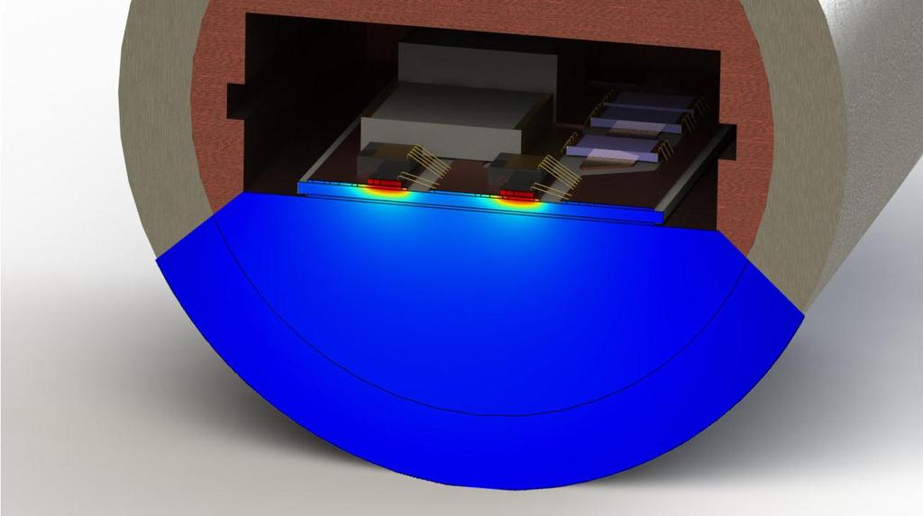
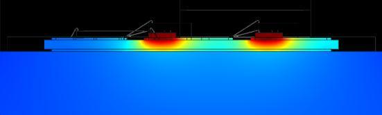
18 Case study Temperature distribution

19 Case Study Temperature distribution Cu-Sn SLID Duraclo 4703 P = 10 W P = 20 W

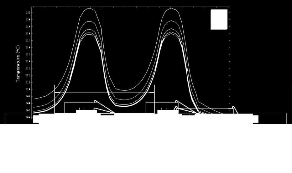
20 Case study Temperature drop
21 Case study Temperature drop 10 W SiC BJT T 1 C Die attach (Au-Sn SLID) T < 0.5 C Substrate T 8 C & 7 C TIM: Power card T <0.5 C & 5 C Cu-Sn SLID Duralco 4703 Base plate T 2-3 C TIM: Graphite-oil T < 0.5 C Shell T < 0.5 C Ambient T 5 C SiC BJT Ambient
22 Case study Temperature drop 20 W Substrate T 15 C & 15 C TIM Power card T <0.5 C & 14 C Ambient T 9 C SiC BJT Ambient


23 Case study Derating of TIM specs

24 Case study Temperature profile
25 Potential life time A small reduction in operation temperature may provide a significant improvement in reliability and lifetime of a device. M. Watts "Design Considerations for High Temperature Hybrid Manufacturability". HiTEC 2008
26 Concluding remarks SLID bonding show great TIM potential for high reliability, performance and temperature applications. Primarily due to: Low thermal resistance. Uniform joint (low "contact resistance"). HT stability and reliability Mechanically robust Further investigations of SLID bonding as a TIM is needed. Applicability for larger and more irregular surfaces.


27 Acknowledgements The HTPEP project and its sponsors and partners My co-authors Torleif A. Tollefsen Olav Storstrøm
28 Thanks for your attention! HTPEP Andreas Larsson SINTEF ICT. Instrumentation dept.
Novel Technique for Flip Chip Packaging of High power Si, SiC and GaN Devices. Nahum Rapoport, Remtec, Inc.
 Novel Technique for Flip Chip Packaging of High power Si, SiC and GaN Devices Nahum Rapoport, Remtec, Inc. 1 Background Electronic Products Designers: under pressure to decrease cost and size Semiconductor
Power Electronics Packaging Solutions for Device Junction Temperature over 220 o C
 EPRC 12 Project Proposal Power Electronics Packaging Solutions for Device Junction Temperature over 220 o C 15 th August 2012 Page 1 Motivation Increased requirements of high power semiconductor device
DITF ToolKit 1. Standard Substrate Sizes (selected at the factory for optimum process)
") DITF ToolKit 1 DITF Toolkit Substrates Common Substrate Materials Alumina (99.5% min) єr = 9.9 Tan d = 1.5 x10⁻⁴ Aluminum Nitride (K170) єr = 8.9 Tan d = 2.0 x10⁻³ Beryllia (99.5%) єr = 6.7 Tan d = 3.0
DITF ToolKit 1 DITF Toolkit Substrates Common Substrate Materials Alumina (99.5% min) єr = 9.9 Tan d = 1.5 x10⁻⁴ Aluminum Nitride (K170) єr = 8.9 Tan d = 2.0 x10⁻³ Beryllia (99.5%) єr = 6.7 Tan d = 3.0
A Novel Thermal Management Approach for Packaging of High Power GaN Devices
 A Novel Thermal Management Approach for Packaging of High Power GaN Devices April 6 th, 2016 1 000304 Agenda - Thermal Management Flange and Package Materials - GaN High Power Densities and the New RF
Packaging Technologies for SiC Power Modules
 Packaging Technologies for SiC Power Modules Masafumi Horio Yuji Iizuka Yoshinari Ikeda ABSTRACT Wide bandgap materials such as silicon carbide (SiC) and gallium nitride (GaN) are attracting attention
Advanced Power Module Packaging for increased Operation Temperature and Power Density
 15th International Power Electronics and Motion Control Conference, EPE-PEMC 2012 ECCE Europe, Novi Sad, Serbia Advanced Power Module Packaging for increased Operation Temperature and Power Density Peter
CX Thin Fil s. Resistors Attenuators Thin-Film Products Thin-Film Services. ISO 9001:2008 RoHS/REACH Compliant ITAR Compliant
 CX Thin Fil s Resistors Attenuators Thin-Film Products Thin-Film Services www.cxthinfilms.com ISO 9001:2008 RoHS/REACH Compliant ITAR Compliant www.cxthinfilms.com sales@cxthinfilms.com +1 (401) 461-5500
NEW DEVELOPMENTS OF DIRECT BONDING ON NON-PRECIOUS METAL SURFACES BY PRESSURE SILVER SINTERING
 NEW DEVELOPMENTS OF DIRECT BONDING ON NON-PRECIOUS METAL SURFACES BY PRESSURE SILVER SINTERING IMAPS-UK Die Attach Workshop 22 November 2018 MTC, Coventry Ly May Chew, Wolfgang Schmitt Heraeus Electronics
curamik CERAMIC SUBSTRATES AMB technology Design Rules Version #04 (09/2015)
") curamik CERAMIC SUBSTRATES AMB technology Design Rules Version #04 (09/2015) Content 1. Geometric properties 1.01. Available ceramic types / thicknesses... 03 1.02. thicknesses (standard)... 03 3. Quality
curamik CERAMIC SUBSTRATES AMB technology Design Rules Version #04 (09/2015) Content 1. Geometric properties 1.01. Available ceramic types / thicknesses... 03 1.02. thicknesses (standard)... 03 3. Quality
Novel Approaches to Thermal Management for Power LED Packaging
 50 Novel Approaches to Thermal Management for Power LED Packaging Thermal management is crucial for the efficiency and reliability of LED products which have become very popular during the past few years.
NanoFoil Technology: Formation Reactions & Thermite Reactions
 NanoBond : Target Bonding for Optimum Sputtering Performance Alan Duckham Reactive NanoTechnologies Reactive NanoTechnologies, Inc. (RNT) 111 Lake Front Drive Hunt Valley, MD 21030 (p) 410.771.9801 (f)
Processor Performance, Packaging and Reliability Utilizing a Phase Change Metallic Alloy Thermal Interface System
 Processor Performance, Packaging and Reliability Utilizing a Phase Change Metallic Alloy Thermal Interface System Chris G. Macris, Thomas R. Sanderson, Robert G. Ebel, Christopher B. Leyerle Enerdyne Solutions,
A New Thermal Management Material for HBLEDs based on Aluminum Nitride Ceramics
 A New Thermal Management Material for HBLEDs based on Aluminum Nitride Ceramics Thermal Management Challenges in HBLED Excess heat leads to a whole range of performance and reliability issues for high
Gold to gold thermosonic bonding Characterization of bonding parameters
 Gold to gold thermosonic bonding Characterization of bonding parameters Thi Thuy Luu *1, Hoang-Vu Nguyen 1, Andreas Larsson 2, Nils Hoivik 1 and Knut E.Aasmundtveit 1 1: Institute of Micro and Nanosystems
Flexible Substrates for Smart Sensor Applications
 Flexible Substrates for Smart Sensor Applications A novel approach that delivers miniaturized, hermetic, biostable and highly reliable smart sensor modules. AUTHORS Dr. Eckardt Bihler, Dr. Marc Hauer,
Metal bonding. Aida Khayyami, Kirill Isakov, Maria Grigoreva Miika Soikkeli, Sample Inkinen
 Metal bonding Aida Khayyami, Kirill Isakov, Maria Grigoreva Miika Soikkeli, Sample Inkinen Timing (delete before presentation) Introduction (Outline, available bonding techniques, evaluation of metal bondings)-3
Die Attach Materials. Die Attach G, TECH. 2U. TECHNICAL R&D DIV.
 Die Attach Materials Die Attach G, TECH. 2U. TECHNICAL R&D DIV. 2 Topics 3 What it is X 5,000 X 10,000 X 50,000 Si Chip Au Plating Substrate Ag Resin 4 Current Products Characteristics H9890-6A H9890-6S
Ag Sinter Joining for WBG Interconnects
 2016 3D-PEIM, June 14, 2016 Ag Sinter Joining for WBG Interconnects Katsuaki Suganuma, Shoji Nagao, Toru Sugahara, Hao Zhang, and Jinting Jiu ISIR, Osaka University, Osaka, Japan SiC Cu Si 3 N 4 Ag SMB
EFFECT OF THERMAL AGING ON THE IMC LAYER BETWEEN SnAgSb SOLDER AND Cu SUBSTRATE. Universiti Kebangsaan Malaysia, 43600, Bangi, Selangor, Malaysia
 EFFECT OF THERMAL AGING ON THE IMC LAYER BETWEEN SnAgSb SOLDER AND Cu SUBSTRATE W. Shualdi 1, I. Ahmad 1, G. Omar 2 and A. Isnin 3 1 Department of Electrical, Electronic and System, Faculty of Engineering,
VTC VM365830VSJ Pre-Amp
 Construction Analysis VTC VM365830VSJ Pre-Amp Report Number: SCA 9708-549 Global Semiconductor Industry the Serving Since 1964 17350 N. Hartford Drive Scottsdale, AZ 85255 Phone: 602-515-9780 Fax: 602-515-9781
Jacques Matteau. NanoBond Assembly: A Rapid, Room Temperature Soldering Process. Global Sales Manager. indium.us/f018
 Jacques Matteau Global Sales Manager NanoBond Assembly: A Rapid, Room Temperature Soldering Process jmatteau@indium.com indium.us/f014 indium.us/f018 Terminology A few key terms NanoFoil is the heat source
PCB Technologies for LED Applications Application note
 PCB Technologies for LED Applications Application note Abstract This application note provides a general survey of the various available Printed Circuit Board (PCB) technologies for use in LED applications.
Future Electronic Devices Technology in Cosmic Space and Electroless Ni/Pd/Au Plating for High Density Semiconductor Package Substrate
 JAXA 25 rd Microelectronics Workshop Future Electronic Devices Technology in Cosmic Space and Electroless Ni/Pd/Au Plating for High Density Semiconductor Package Substrate November 2, 2012 Yoshinori Ejiri
High-Temperature-Resistant Interconnections Formed by Using Nickel Micro-plating and Ni Nano-particles for Power Devices
 Kato et al.: High-Temperature-Resistant Interconnections (1/6) [Technical Paper] High-Temperature-Resistant Interconnections Formed by Using Nickel Micro-plating and Ni Nano-particles for Power Devices
Secure Attachment in Pulsed Power Applications
 Secure Attachment in Pulsed Power Applications Michael R. Ehlert Director of Process Engineering Dr. Peter Barnwell European Business Manager Ronald H. Schmidt V. P. Engineering and Technology Phillip
Power Electronics Packaging Revolution Module without bond wires, solder and thermal paste
 SEMIKRON Pty Ltd 8/8 Garden Rd Clayton Melbourne 3168 VIC Australia Power Electronics Packaging Revolution Module without bond wires, solder and thermal paste For some years now, the elimination of bond
Thermally Functionalized Structural Materials for Consumer Devices Aaron Vodnick
 Thermally Functionalized Structural Materials for Consumer Devices Aaron Vodnick IMAPS NE May 2015 Overview Our focus is a material to more effectively dissipate heat TIMs Chip Substrate Heat Sink Heat
Extremely High Temperature and High Pressure (x-hthp) Endurable SOI Device and Sensor Packaging for Harsh Environment Applications
 Endurable SOI Device and Sensor Packaging for Harsh Environment Applications") Extremely High Temperature and High Pressure (x-hthp) Endurable SOI Device and Sensor Packaging for Harsh Environment Applications K.Y.Au*, F.X. Che, Eva Wai Leong Ching v Institute of Microelectronics,
Extremely High Temperature and High Pressure (x-hthp) Endurable SOI Device and Sensor Packaging for Harsh Environment Applications K.Y.Au*, F.X. Che, Eva Wai Leong Ching v Institute of Microelectronics,
PASSIVE COMPONENT MATERIALS HIMEC, UNIMEC, OHMCOAT
 PASSIVE COMPONENT MATERIALS HIMEC, UNIMEC, OHMCOAT PRODUCT RANGE Sintering Materials =>> HIMEC Used for Electrodes on Passive Components For Photovoltaic Pastes (Front Side & Back Side Silver Paste ) For
Basic Properties and Application Examples of
 Basic Properties and Application Examples of 1. Basic properties of PGS 2. Functions of PGS 3. Application Examples Presentation [Sales Liaison] Panasonic Electronic Devices Co., Ltd. Capacitor Business
High Temperature, High Power Module Design for Wide Bandgap Semiconductors: Packaging Architecture and Materials Considerations
 High Temperature, High Power Module Design for Wide Bandgap Semiconductors: Packaging Architecture and Materials Considerations Z. John Shen, Brian Grummel, Ryan McClure, Ali Gordon, and Allen Hefner*
High temperature reliability of power module substrates
 High temperature reliability of power module substrates Dean Hamilton, University of Warwick, United Kingdom, d.p.hamilton@warwick.ac.uk Liam Mills, TT Electronics Semelab Ltd, Lutterworth, UK, Liam.Mills@semelab-tt.com
Keeping Cool!: selecting high performance thermal materials for LED Lighting applications. Ian Loader 25/03/14
 Keeping Cool!: selecting high performance thermal materials for LED Lighting applications Ian Loader 25/03/14 1 Target Points to cover Basics of Thermal Management Considerations for thermal materials
Optimized Thermal Management. with Advanced Ceramic Materials for Power Electronics, CPV and HCPV
 Optimized Thermal Management with Advanced Ceramic Materials for Power Electronics, CPV and HCPV T H E C E R A M I C E X P E R T S Ceramic Base Materials for the Electronics Industry We offer the full
AlSiC for Optoelectronic Thermal Management and Packaging Designs
 for Optoelectronic Thermal Management and Packaging Designs Mark A. Occhionero, Richard W. Adams, Dave Saums Ceramics Process Systems Chartley, MA 02712-0338 Abstract Aluminum silicon carbide () metal
Reliability of Interconnects in LED Lighting Assemblies Utilizing Metal Clad Printed Circuit Boards Stefano Sciolè BDM I.M.S.
 Reliability of Interconnects in LED Lighting Assemblies Utilizing Metal Clad Printed Circuit Boards Stefano Sciolè BDM I.M.S. Henkel Electronic Materials Agenda 1. Introduction 2. Motivation 3. Interconnect
LED Die Attach Selection Considerations
 LED Die Attach Selection Considerations Gyan Dutt & Ravi Bhatkal Alpha, An Alent plc Company Abstract Die attach material plays a key role in performance and reliability of mid, high and super-high power
V I S H AY I N T E R T E C H N O L O G Y, I N C. Vishay Electro-Films. w w w. v i s h a y. c o m
 V I S H AY I N T E R T E C H N O L O G Y, I N C. Pattern Substrates Using Thin Film Technology Vishay Electro-Films Application-Specific Pattern Substrates P r e c i s i o n R e s i s t o r s C a p a b
Maximum MAX662 12V DC-DC Converter
 Construction Analysis Maximum MAX662 12V DC-DC Converter Report Number: SCA 9512-445 Global Semiconductor Industry the Serving Since 1964 17350 N. Hartford Drive Scottsdale, AZ 85255 Phone: 602-515-9780
All-Polyimide Thermal Interface Products
 All-Polyimide Thermal Interface Products SMTA Harsh Environment Electronics Workshop Dearborn, MI 6/24/03 Jim Fraivillig Fraivillig Technologies Boston, MA Why polyimide? HARSH ENVIRONMENT ELECTRONICS.
RoHS Compliance Document
 D-Pak RoHS Compliance Document Contents: 1. 2. Solder Reflow 3. Tin Whisker Report D-pak BOM 1 Chip Silicon.713 Si 744-21-3.713 1% 1.9% Encapsulant Epoxy Resin.11419 Lead Frame Copper.244 Die Attach Soft
FYS4260/FYS9260: Microsystems and Electronics Packaging and Interconnect. Metallization and Interconnects
 FYS4260/FYS9260: Microsystems and Electronics Packaging and Interconnect Metallization and Interconnects Learning objectives Metal heros Significance of selecting right metallization systems and examples
Enhanced Thermal Conductivity of Polyimide Films via a Hybrid of Micro- and Nano-Sized Boron Nitride
 The 2012 World Congress on Advances in Civil, Environmental, and Materials Research (ACEM 12) Seoul, Korea, August 26-30, 2012 Enhanced Thermal Conductivity of Polyimide Films via a Hybrid of Micro- and
Thermal Symposium August Minteq International, Inc. Pyrogenics Group A Thermal Management Solution for State-of-the-Art Electronics
 Thermal Symposium August 9-10 2017 Minteq International, Inc. Pyrogenics Group A Thermal Management Solution for State-of-the-Art Electronics Mark Breloff Technical Sales Manager 1 Electronics power requirements
EPO-TEK Selector Guide
 Selector Guide www.epotek.com Electrically & Thermally Conductive Thermally Conductive/Electrically Insulating Optical/Fiber Optic Innovative Epoxy Adhesive Solutions for Over 45 Years Electrically & Thermally
Ni Sn Solid-Liquid Interdiffusion (SLID) Bonding for Thermo-Electric Elements in Extreme Environments FEA of the joint stress
 Bonding for Thermo-Electric Elements in Extreme Environments FEA of the joint stress") Ni Sn Solid-Liquid Interdiffusion (SLID) Bonding for Thermo-Electric Elements in Extreme Environments FEA of the joint stress Andreas Larsson* 1,2, Torleif A. Tollefsen 3, Ole Martin Løvvik 4 and Knut
Ni Sn Solid-Liquid Interdiffusion (SLID) Bonding for Thermo-Electric Elements in Extreme Environments FEA of the joint stress Andreas Larsson* 1,2, Torleif A. Tollefsen 3, Ole Martin Løvvik 4 and Knut
High Efficiency UV LEDs Enabled by Next Generation Substrates. Whitepaper
 High Efficiency UV LEDs Enabled by Next Generation Substrates Whitepaper Introduction A primary industrial market for high power ultra-violet (UV) LED modules is curing equipment used for drying paints,
Investigation on the development of intermetallic phases in electrodeposited lead-free solder Au/Sn based stacks
 Investigation on the development of intermetallic phases in electrodeposited lead-free solder / based stacks Io Mizushima and Peter Torben Tang IPU, Denmark outlooks 1. Introduction 2. Experimental procedure
Materials Declaration Form
 Materials Declaration Form IPC 1752 Version 2 Form Type * Distribute Sectionals * Material Info Subsectionals * A-D Manufacturing Info * : Required Field Supplier Information Company Name * STMicroelectronics
HBLED packaging is becoming one of the new, high
 Ag plating in HBLED packaging improves reflectivity and lowers costs JONATHAN HARRIS, President, CMC Laboratories, Inc., Tempe, AZ Various types of Ag plating technology along with the advantages and limitations
Thermal Management Materials for PCBs used in Power Electronics
 Thermal Management Materials for PCBs used in Power Electronics Sandy Kumar, Ph.D. Director of Technology American Standard Circuits, Inc. 3615 Wolf Road, Franklin Park, IL 60131 Phone: 847-455-1500, Fax:
Rockwell R RF to IF Down Converter
 Construction Analysis Rockwell R6732-13 RF to IF Down Converter Report Number: SCA 9709-552 Global Semiconductor Industry the Serving Since 1964 17350 N. Hartford Drive Scottsdale, AZ 85255 Phone: 602-515-9780
ROHS Compliant. Description. General Specifications. Resistive Element Substrate Terminal Finish Operating Temperature. Electrical Specifications
 ROHS Compliant Model B100NA20X4 Chip Attenuator 100 Watts, 20 db Description The B100NA20X4 is high performance Aluminum Nitride (AlN) chip attenuator intended as a cost competitive alternative to Beryllium
Materials Declaration Form
 Materials Declaration Form IPC 1752 Form Type * Distribute Version Sectionals * Material Info Subsectionals * Manufacturing Info * : Required Field 2 A-D Supplier Information Company Name * STMicroelectronics
Chin C. Lee Electrical Engineering & Computer Science Materials and Manufacturing Technology University of California, Irvine
 IEEE CPMT OC Chapter s Inaugural Technical meeting Sept. 20, 2011 Silver Flip-chip Interconnect Technology Chin C. Lee Electrical Engineering & Computer Science Materials and Manufacturing Technology University
Materials Declaration Form
 Materials Declaration Form IPC 1752 Version 2 Form Type * Distribute Sectionals * Material Info Subsectionals * A-D Manufacturing Info * : Required Field Supplier Information Company Name * STMicroelectronics
February Thermal Interface Material performance comparison
 ZODIAC DATA SYSTEMS Thermal Interface Material performance comparison Alexis de BIBIKOFF Sandrine LELONG-FENEYROU February 2012 February 2012 Thermal Interface Material performance comparison Overview
PL ISSN 0209-Ü058 MATERIAŁY ELEKTRONICZNE T NR 3 JOINING HEATSINK COMPOSITE MATERIALS TO CERAMICS*
 PL ISSN 0209-Ü058 MATERIAŁY ELEKTRONICZNE T. 30-2002 NR 3 JOINING HEATSINK COMPOSITE MATERIALS TO CERAMICS* Katarzyna Pietrzak", Dariusz Kaliński' The special kind of MMCs (carbon fibre or tungsten particle
Materials Declaration Form
 Materials Declaration Form IPC 1752 Version 2 Form Type * Distribute Sectionals * Material Info Subsectionals * A-D Manufacturing Info * : Required Field Supplier Information Company Name * STMicroelectronics
Building HDI Structures using Thin Films and Low Temperature Sintering Paste
 Building HDI Structures using Thin Films and Low Temperature Sintering Paste Catherine Shearer, James Haley and Chris Hunrath Ormet Circuits Inc. - Integral Technology California, USA chunrath@integral-hdi.com
Finite Element Analysis of a High Power Resistor
 Barry Industries, Inc. Finite Element Analysis of a High Power Resistor prepared by: Barry Industries, Inc. date: 07 April 1996 . Finite Element Analysis of a High Power Termination Table of Contents Table
Fixed Resistors INSULATED ALUMINUM SUBSTRATES. Thermal Solutions for Hi Brightness LED Applications - Application Note
 INSULATED ALUMINUM SUBSTRATES TT electronics is a leading designer and manufacturer of electronic components. As a result of our experience with power components, Anotherm substrates were developed as
3M XYZ / Isotropic Electrically Conductive Adhesive Transfer Tape 9709
 Technical Data October, 2009 3M XYZ / Isotropic Electrically Conductive Adhesive Transfer Tape 9709 Product Description 3M XYZ/Isotropic Electrically Conductive Adhesive Transfer Tape 9709 is a pressure
Australian Journal of Basic and Applied Sciences. Pb-Free Solder Ball Robustness Comparison under AC and TC Reliability Test
 AENSI Journals Australian Journal of Basic and Applied Sciences ISSN:1991-8178 Journal home page: www.ajbasweb.com Pb-Free Solder Ball Robustness Comparison under AC and TC Reliability Test 1,2 Tan Cai
EP A2 (19) (11) EP A2 (12) EUROPEAN PATENT APPLICATION. (43) Date of publication: Bulletin 2006/23
 (11) EP A2 (12) EUROPEAN PATENT APPLICATION. (43) Date of publication: Bulletin 2006/23") (19) Europäisches Patentamt European Patent Office Office européen des brevets (12) EUROPEAN PATENT APPLICATION (11) EP 1 667 226 A2 (43) Date of publication: 07.06.06 Bulletin 06/23 (1) Int Cl.: H01L
(19) Europäisches Patentamt European Patent Office Office européen des brevets (12) EUROPEAN PATENT APPLICATION (11) EP 1 667 226 A2 (43) Date of publication: 07.06.06 Bulletin 06/23 (1) Int Cl.: H01L
Fraunhofer IZM Berlin
 Fraunhofer IZM Berlin Advanced Packaging for High Power LEDs Dr. Rafael Jordan SIIT Agenda Gluing Soldering Sintering Transient Liquid Phase Bonding/Soldering Thermo Compression Junction Temperature Measurements
Composite Materials. Metal matrix composites
 Composite Materials Metal matrix composites Introduction The properties that make MMCs attractive are high strength and stiffness, good wear resistance, high service temperature, tailorable coefficient
Environmental Management and Materials Information
 Environmental Management and Materials Information Product Content Information for: MAX3622CUE+ Links Qualifications Package Description Chemical Composition Detailed Package Component Data Qualifications
Features Conductive Room Temperature Cure. Product Ref IP 4525IP Low viscosity adhesive & coating. High thermal conductivity
 Properties and Part Selection Overview Selection Table - Epoxy-Based Adhesive Properties Features Conductive Room Temperature Cure Product Ref 120 132 4461IP 42IP 438 700 Properties High electrical conductivity
Modeling Printed Circuit Boards with Sherlock 3.2
 Modeling Printed Circuit Boards with Sherlock 3.2 DfR Solutions September 23, 2014 Presented by: Dr. Nathan Blattau Senior Vice President 9000 Virginia Manor Rd Ste 290, Beltsville MD 20705 301-474-0607
ROLINX Laminated Busbar. Design Rules Version 01 (12/2015)
") ROLINX Laminated Busbar Design Rules Version 01 (12/2015) Content 1. Introduction... 03 7. Features... 13 2. Configuration...03 8. Thermal parameters... 14 3. Products... 04 9. General parameters... 14
ROLINX Laminated Busbar Design Rules Version 01 (12/2015) Content 1. Introduction... 03 7. Features... 13 2. Configuration...03 8. Thermal parameters... 14 3. Products... 04 9. General parameters... 14
MATERIALS REQUIREMENTS FOR OPTOELECTRONIC PACKAGING -- FIBER SOLDERING
 MATERIALS REQUIREMENTS FOR OPTOELECTRONIC PACKAGING -- FIBER SOLDERING Fahong Jin Spring 2003 TABLE OF CONTENTS 1. INTRODUCTION 2. OPTICAL FIBER METALLIZATION 3. SOLDER SELECTION FOR FIBER JOINT 4. FEEDTHROUGH
Lecture 7. Lecture 7. Characterization of Components. Cooling at Component Level. Cooling at Component Level. Cooling at Component Level
 Characterization of Components Hans Jonsson Heat flow from chip to heat sink - Thermal Component Models Interface resistance (Contact resistance) TIM Thermal Interface Materials Project assignment The
Nanosilver Paste: an Enabling Nanomaterial for Low-temperature Joining of Power Devices
 G-Q. Lu presentation at 2011 APEC Annual Meeting (3/2011) 1 Nanosilver Paste: an Enabling Nanomaterial for Low-temperature Joining of Power Devices Guo-Quan (GQ) Lu, Professor Dept. of MSE and ECE, Virginia
Meet the Demands of High-Temperature Applications With Thin Film Resistors
 Page 1 of 7 Meet the Demands of High-Temperature Applications With Thin Film Resistors By Dr. Claude Flassayer, Vishay/Sfernice Thin Film Division, www.vishay.com Thursday, September 30, 2010 The demands
*EP A2* EP A2 (19) (11) EP A2 (12) EUROPEAN PATENT APPLICATION. (43) Date of publication: Bulletin 2005/08
 (11) EP A2 (12) EUROPEAN PATENT APPLICATION. (43) Date of publication: Bulletin 2005/08") (19) Europäisches Patentamt European Patent Office Office européen des brevets *EP00891A2* (11) EP 1 08 91 A2 (12) EUROPEAN PATENT APPLICATION (43) Date of publication: 23.02.0 Bulletin 0/08 (1) Int Cl.
(19) Europäisches Patentamt European Patent Office Office européen des brevets *EP00891A2* (11) EP 1 08 91 A2 (12) EUROPEAN PATENT APPLICATION (43) Date of publication: 23.02.0 Bulletin 0/08 (1) Int Cl.
Mosel Vitelic MS62256CLL-70PC 256Kbit SRAM
 Construction Analysis Mosel Vitelic MS62256CLL-70PC 256Kbit SRAM Report Number: SCA 9703-499 Global Semiconductor Industry the Serving Since 1964 17350 N. Hartford Drive Scottsdale, AZ 85255 Phone: 602-515-9780
Free Electron Model What kind of interactions hold metal atoms together? How does this explain high electrical and thermal conductivity?
 Electrical Good conductors of heat & electricity Create semiconductors Oxides are basic ionic solids Aqueous cations (positive charge, Lewis acids) Reactivity increases downwards in family Mechanical Lustrous
Fraunhofer ENAS Current results and future approaches in Wafer-level-packaging FRANK ROSCHER
 Fraunhofer ENAS - Current results and future approaches in Wafer-level-packaging FRANK ROSCHER Fraunhofer ENAS Chemnitz System Packaging Page 1 System Packaging Outline: Wafer level packaging for MEMS
Chapter 3 Silicon Device Fabrication Technology
 Chapter 3 Silicon Device Fabrication Technology Over 10 15 transistors (or 100,000 for every person in the world) are manufactured every year. VLSI (Very Large Scale Integration) ULSI (Ultra Large Scale
Copyright 2008 Year IEEE. Reprinted from IEEE ECTC May 2008, Florida USA.. This material is posted here with permission of the IEEE.
 Copyright 2008 Year IEEE. Reprinted from IEEE ECTC 2008. 27-30 May 2008, Florida USA.. This material is posted here with permission of the IEEE. Such permission of the IEEE does not in any way imply IEEE
Effect of Die Bonding Condition for Die Attach Film Performance in 3D QFN Stacked Die.
 Effect of Die Bonding Condition for Die Attach Film Performance in 3D QFN Stacked Die. A. JALAR, M. F. ROSLE, M. A. A. HAMID. School of Applied Physics, Faculty of Science and Technology Universiti Kebangsaan
Materials Declaration Form
 Materials Declaration Form IPC 1752 Version 2 Form Type * Distribute Sectionals * Material Info Subsectionals * A-D Manufacturing Info * : Required Field Supplier Information Company Name * STMicroelectronics
Anisotropic Conductive Adhesives with Enhanced Thermal Conductivity for Flip Chip Applications
 Anisotropic Conductive Adhesives with Enhanced Thermal Conductivity for Flip Chip Applications Myung-Jin Yim, Jin-Sang Hwang and Jin-Gu Kim ACA/F Dept., Telephus, Inc. 25-11, Jang-dong, Yusong-gu, Taejon
Environmental Management and Materials Information
 Environmental Management and Materials Information Product Content Information for: MAX3637ETM+ Links Qualifications Package Description Chemical Composition Detailed Package Component Data Qualifications
Performance and Reliability Characteristics of 1200 V, 100 A, 200 o C Half-Bridge SiC MOSFET-JBS Diode Power Modules
 Performance and Reliability Characteristics of 1200 V, 100 A, 200 o C Half-Bridge SiC MOSFET-JBS Diode Power Modules James D. Scofield and J. Neil Merrett Air Force Research Laboratory 1950 Fifth St WPAFB,
Mechanical Properties and Microstructure of Pure Copper Joints Brazed with Amorphous Cu68.5Ni15.7Sn9.3P6.5 Filler Metal
 Mechanical Properties and Microstructure of Pure Copper Joints Brazed with Amorphous Cu68.5Ni15.7Sn9.3P6.5 Filler Metal Jing Zhang 1,*, Weiyuan Yu 2, Wenjiang Lu 2 1 School of Physics and Mechanical-Electrical
Challenges for Embedded Device Technologies for Package Level Integration
 Challenges for Embedded Device Technologies for Package Level Integration Kevin Cannon, Steve Riches Tribus-D Ltd Guangbin Dou, Andrew Holmes Imperial College London Embedded Die Technology IMAPS-UK/NMI
How Bad's the Damage?
 How Bad's the Damage? Evaluating Probe Damage On Aluminum, Solder, Gold, UBM, and Copper Pads. Ken Smith Vice President of Technology Development Pyramid Probe Division, Cascade Microtech Goal of Presentation
Pressure-Assisted Low-Temperature Sintering of Silver Paste as an Alternative Die-Attach Solution to Solder Reflow
 Pressure-Assisted Low-Temperature Sintering of Silver Paste as an Alternative Die-Attach Solution to Solder Reflow Zhiye (Zach) Zhang and Guo-Quan Lu Center for Power Electronics Systems The Bradley Department
nicrom e l e c t r o n i c
 G E N E R A L High Performance Thick Film Resistors C A T A L O G 3 Nicrom Electronic Via Roncaglia CH - 6883 Novazzano SWITZERLAND Phone : ++4 () 9 68 99 86 Fax : ++4 () 9 68 99 86 info@nicrom-electronic.com
c/bach, 2-B Pol. Ind Foinvasa Montcada i Reixac (Barcelona) SPAIN Tel FAX
 SPAIN Tel FAX") 1- What is 2- How does it work? 3- How do we make it? 4- Applications 5- Processing? WHAT IS? Thick aluminium based substrate, cladded in ED copper foil. Designed for an effective thermal dissipation and
1- What is 2- How does it work? 3- How do we make it? 4- Applications 5- Processing? WHAT IS? Thick aluminium based substrate, cladded in ED copper foil. Designed for an effective thermal dissipation and
Materials Declaration Form
 Materials Declaration Form IPC 1752 Version 2 Form Type * Distribute Sectionals * Material Info Subsectionals * A-D Manufacturing Info * : Required Field Supplier Information Company Name * STMicroelectronics
Materials Declaration Form
 Materials Declaration Form IPC 1752 Version 2 Form Type * Distribute Sectionals * Material Info Subsectionals * A-D Manufacturing Info * : Required Field Supplier Information Company Name * STMicroelectronics
3D technologies for integration of MEMS
 3D technologies for integration of MEMS, Fraunhofer Institute for Electronic Nano Systems Folie 1 Outlook Introduction 3D Processes Process integration Characterization Sample Applications Conclusion Folie
Future Electronic Devices Technology in Cosmic Space and Lead-free Solder Joint Reliability
 The 22nd Microelectronics Work Future Electronic Devices Technology in Cosmic Space and Lead-free Solder Joint Reliability Key Points (1) High Speed Solder Ball Shear Test (2) Relationship between Surface
Nano-Micro Particle Filled Thermal Interface Materials: Towards Materials Development, Characterization, Assembly, and Performance Evaluation
 Nano-Micro Particle Filled Thermal Interface Materials: Towards Materials Development, Characterization, Assembly, and Performance Evaluation Rabindra N. Das, Evan Chenelly, Erich Kopp, Dave Alcoe, Mark
HIGH TEMPERATURE CERAMIC & GRAPHITE ADHESIVES
 HIGH TEMPERATURE & GRAPHITE S Technical Bulletin A2 Ceramabond 835-M bonds halogen lamp. Ceramabond 503 coats heater used to 1700 ºC. Ceramabond 685-N bonds infrared heater. Graphi-Bond 551-RN bonds graphite
1 Thin-film applications to microelectronic technology
 1 Thin-film applications to microelectronic technology 1.1 Introduction Layered thin-film structures are used in microelectronic, opto-electronic, flat panel display, and electronic packaging technologies.
Microelectronics Devices
 Microelectronics Devices Yao-Joe Yang 1 Outline Basic semiconductor physics Semiconductor devices Resistors Capacitors P-N diodes BJT/MOSFET 2 Type of Solid Materials Solid materials may be classified