VOIDS IN SOLDER JOINTS. Raiyo Aspandiar Intel Corporation
|
|
|
- Cory Richards
- 5 years ago
- Views:
Transcription
1 VOIDS IN SOLDER JOINTS Raiyo Aspandiar Intel Corporation Presented at SMTA Boise Expo and Tech Forum, March 20, 2018
2 Contents Introduction to Solder Voids Various Types of Voids Description Detection Root Causes Ways of mitigating Summary 2

3 What is a Solder Joint Void? Typical BGA Solder Joint with a large Void Solder Joint Void o A void is an absence of solder within a solder joint o A void typically contains nothing but air o Some voids contain flux residues or cured resins when epoxy fluxes or resin containing pastes are used 3
4 Why do we care about Voids? Some types of Voids deleteriously impact Solder Joint Reliability Voids reduce the thermal conductivity of the solder joints Voids can cause solder bridges Voids can cause solder transfer between neighboring solder joints during the reflow soldering process In small solder joints, voids can significantly reduce their current carrying capacity 4
5 Types of Voids Macro Voids Planar Microvoids Shrinkage Voids Micro-Via Voids IMC Microvoids Pinhole Microvoids 5


6 MACRO-VOIDS 6
7 Description - Macrovoids Voids generated by the evolution of volatile ingredients of fluxes and solder pastes Insufficient time to escape 100 to 300 µm (4 to 12 mils) in diameter Found anywhere in the solder joint Not Just at Land to solder interfaces NOT unique to SnAgCu (LF) solder joints Eutectic SnPb SnBiX Also called Process voids Generally, when SMT process engineers talk about voids in solder joints these are the type of voids that are being referred to 7


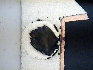
8 Examples of Macrovoids in BGA Solder Joints 8

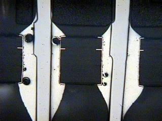
9 Examples of Macrovoids in Through Hole Solder Joints 9
10 Causes of Macro Voids Trapped gases within the solder joint which have insufficient time to escape during the reflow process when the solder is molten Source of these gases Chemical Ingredients of fluxes and solder pastes that evolve during the SMT reflow process when the temperature of the materials is raised above their boiling point Absorbed moisture in the board laminate and lands that evolves above 100C Water vapor resulting from the reduction of Oxides on the surfaces of solder particles in the paste and solder balls as well as on the board lands; These oxides are reduced by the action of the organic acids in the flux 10

11 Inclusion vs Exclusion Macro Voids -- Typically for Gull Wing Solder Joints -- Type Shape(s) Causes Inclusion Exclusion Spherical, elliptical, Cigar-shaped Irregular shapes Trapped gases Squeeze out of solder paste, hot tearing, ductile rupture Images and Exclusion Voids concept from T.L. Lewis, C.O. Ndiaye and J.R. Wilcox, Inclusion Voiding in Gull Wing Solder Joints, APEX EXPO Proceeding, 2012 Exclusion Macro Voids have causes different from typical macro voids 11
12 Areas Critical to Macro Void Generation Solder Paste Reflow Soldering Process Printed Circuit Board Component Other Control of Critical Parameters in these areas is essential to minimize Macro Voids 12
13 Solder Paste Parameters Critical to Macro Void Generation Solvent Amount, Boiling Point, Volatility determine the amount of macro voids generated most solvents in the solder paste should evolve at temperatures below the solder alloy melting point to minimize macro-voids Volume printed on Land Larger paste printed volume will result in more macro-voids due to more volume of solvents being present Solder Powder characteristics More oxidized powder results in increased macro voids Flux Higher activity and amount will result in faster, complete reduction of solder oxides which will enable macro voids formed by this reduction reaction more time to escape from the solder joint 13
14 Parameters Critical to Macro Void Generation (continued) Reflow Process Profile Peak Reflow Temperature Higher Temperature lowers solder surface tension and allows more `mobility` for macro voids which can lead to their escape from the solder joint Time Above Liquidus Longer liquidus time increases probability for escape of macro voids from the solder joint Flux Activation Time (also called soak time) Most of volatile chemical compounds in the solder paste are evolved during this period; hence the flux activation time needs to be sufficient for this evolution to happen 14
15 Reflow Process Parameters Critical to Macro Void Generation (continued) Reflow Atmosphere Atmospheres with lower oxygen content produce less amount of oxidation of the solder surfaces during the reflow soldering process Less oxides will result in less macro voids since a. reduction of oxides creates water vapor which is one source of macro voids b. lack of an oxide crust on the other surface of the balls when molten; this oxide crust can prevent voids from escaping from the molten ball during reflow soldering 15
16 PCB and Component Parameters Critical to Macro Void Generation (continued) Surface Finish Co-deposited volatile organic compounds from surface finish plating operations will result in more macro voids Land Size and Design (soldermask defined / metal defined) Oxide Content of Solderable Surface Higher oxide content, typically copper oxides, will result in more macro voids Contamination Contamination can increase amount of macro voids by a) presenting a non-solderable surface on the lands which may keep macro voids attached to the lands and b) by generating volatile gases at soldering temperatures if the contamination decomposes 16

17 Parameters Critical to Macro Void Generation (continued) General Ambient temperature and humidity conditions Excessive temperature and humidity causes oxidation of the solder paste particles and BGA balls Excessive oxidation on solder paste particles and BGA balls leads to excessive macro-voids when these oxides are reduced by the flux during reflow soldering Contamination during board assembly processes This leads to non-wettable patches on the PCB lands Macro voids form at those patches and get stuck at the board interface 17

18 PLANAR MICRO-VOIDS 18

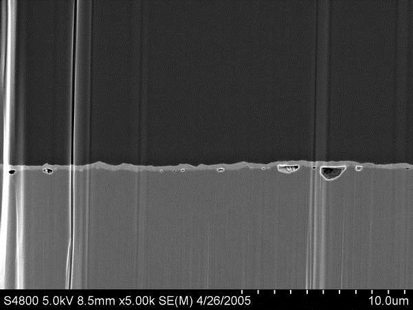
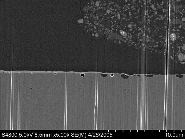
19 Description of Planar Micro Voids Planar Microvoids are smaller than 1-2 mils in diameter Planar Microvoids are located in one plane at the Land-tosolder interface above the Intermetallic compound Planar Microvoids are a risk for reliability failures of BGA and other solder joints Planar Micro Voids BGA Solder Joint Planar Micro Voids Laminate Copper Land 19


20 Detection of Micro Voids Cross-sectional Analysis Pull off solder joint from land Micro voids 20
21 Characteristics of Planar Microvoids Always occur at the land-to-solder joint Interface (PCB Land) Observed predominantly on ImAg surface finishes but also reported with other surface finishes (OSP, ENIG) in the industry Appear to be a PCB batch related phenomena More prevalent on soldermask defined lands (SMD) But also formed on metal defined lands (MD) Does NOT cause yield loss But CAN be a reliability risk 21
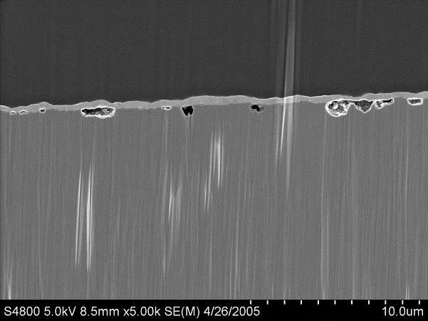
 Copper")

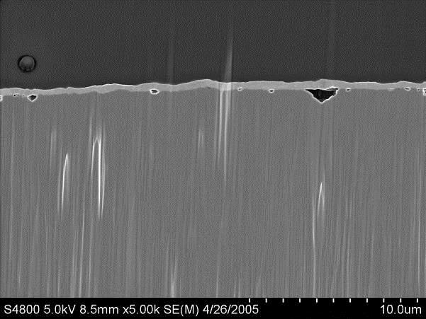
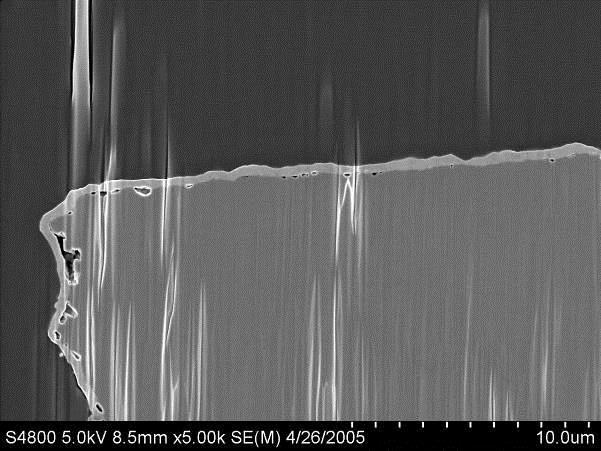
22 Root Cause of Planar Microvoids Caves in the Copper of the PCB Lands under ImAg Surface Finish Plating on as-received PCBs ImAg Roof ImAg Roof Cave Cave Copper Land SEM Photo of XS after FIB (Focused Ion Beam) Copper Land SEM Photo of XS without FIB (Conventional Mechanical Polish) Strong correlation within a PCB lot between Caves in as-received bare boards that exhibited caves and boards that exhibited Planar microvoids after SMT assembly 22

23 PCB Cu Caves Contents As- received PCB SEM XS View EDS Spectra Oxygen(O) was detected within the PCB Cu Caves on the walls and floor under a roof of ImAg Plating. 23
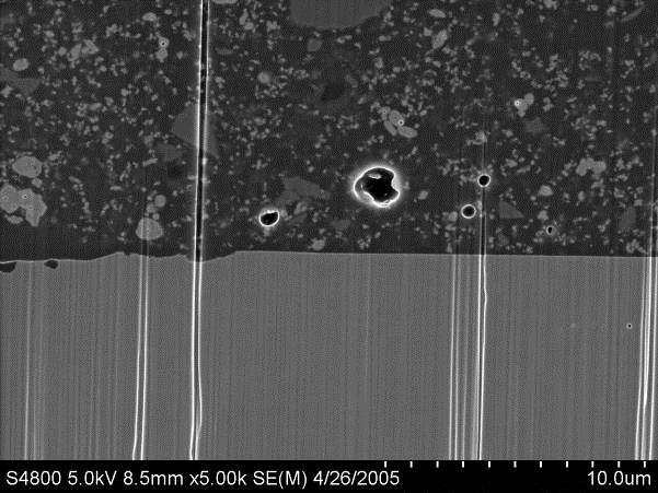
24 More Micrographs Illustrating Presence of Caves under ImAg plating Left -- From the same BGA Land -- Right Many Caves Observed 24


25 Micrographs showing Absence of Caves under ImAg plating From the same BGA Land, but different board lot from one in previous slide Left Right No Caves Observed 25


26 IN-SITU THERMAL X-RAY IMAGING Solder Paste Spheres SAC405 Melts 217C Planar Micro-voids Process Macro-voids Process Macro-voids Planar Micro-voids form ~10 s after Process Macro-voids form 26
27 Temp IMMERSION Ag CAVES TO MICROVOIDS FORMATION MECHANISM Cu CAVES ~1um Flux in the Solder Paste Melts Flux Reacts with Ag Oxides and other Reducible Contaminants on Ag Surface Macro PROCESS Voids Begin Typical Reflow Profile T melting FLUX Process Voids ~150um Macro PROCESS Voids Grow Cu Oxide in CAVES exposed to Flux and are Reduced; Creating MICROVOIDS IMC-Intermetallic Compound Grows Microvoids ~25um IMC Process Voids ~250um Some PROCESS- MICROVOIDS Coalesce and Float-up. Solder Solidifies; Trapping both PROCESS VOIDS & MICROVOIDS IMMERSION Ag Cu CAVES ~1um BGA SOLDER SOLDER PASTE Solder Paste Printed on the PCB Lands BGA Component Placed on the PCB Lands Cu Caves w/ag Roofs Present at PCB Surface Process Voids ~100um Caves Time Cu CAVES ~1um Macro Process Voids Formed Ag Roof Dissolves as Solder Paste + BGA Solder Ball Melts Melted Solder Reacts w/cu and Begin to Form IMC Microvoids ~25um IMC MICROVOIDS Continue to Form IMC Grows at the Expense of Cu IMC Displaces Cu Leaving MICROVOIDS Near IMC Surface Process Voids ~200um 27
28 A Hypothesis for Cave Formation -- Galvanic Corrosion -- Cu +2 Cu 2e- 2Ag+ 2Ag When ImAg plating starts, areas with SM residue or particles are not plated Cu Surface Ag deposits around SM or particle Ag pore or pinhole forms; roughness of copper surface also is a factor Cu +2 2e- Cu Cu Area <<<< Ag Area Galvanic Corrosion Begins Cave under ImAg 2Ag+ 2Ag Top View 28

29 A Hypothesis for Cave Formation -- Galvanic Corrosion -- Cu +2 2e- 2Ag+ 2Ag Top View Cu Ag deposition & Ag build-up continues Cu Cave Ag Roof After ImAg, Cu cave walls get oxidized Soldermask Cu +2 Cu 2e- Cu Galvanic Corrosion Begins 2Ag+ 2Ag Soldermask edge-crevice effect 29
30 Mitigating Planar Microvoids Copper Caves result from Excessive Galvanic Corrosion Cu +2 2e- 2Ag+ 2Ag Cu Excessive Galvanic Corrosion results from a complex interaction of PCB Cu surface condition, PCB geometric design ImAg plating variables: Ag+ concentration, ph, Plating rate and time Hence, a. Proper Micro-etch and Plating Chemistry by the Chemistry Supplier, and b. Strict Control of the Critical to Function Variables during the Plating Process at PCB Fabricator are necessary to lower Risk of Planar Microvoids formation during SMT Assembly 30
31 SHRINKAGE VOIDS 31


32 Description of Shrinkage Voids Elongated, voids with rough, `dendritic` edges emanating from the surface of the solder joints These are seen not just in BGA solder joints, but also in Through Hole Solder Joints and chip component solder joints 32
33 Shrink Hole Void Characteristics Industry consensus is that solidification sequence of SAC solders causes shrink holes Slow Cooling of solder joints causes excessive shrinkage of the final eutectic solder phase just before solidification Disturbance to the solder joint while it is solidifying will increase amount and size of shrinkage voids Do not impact reliability Is not a `Crack` and does not continue to grow under thermomechanical stresses Also called `sink holes` and `hot tears` Shrink Hole Voids are natural for SnAgCu solders, can be minimized 33

34 MICRO-VIA VOIDS 34

35 Micro-Via Voids Voids generated due to the presence of a microvia in the BGA land MicroVia Molten solder has not wet the inside copper walls of the microvia Molten solder has wet the inside copper walls of the microvia but left a void above it 35


36 Diagrammatic Representation of Void Formation due to Microvias in BGA Lands Gases are evolved in the microvia during reflow soldering air from within microvia Water vapor from solder oxide reduction reaction Other volatile compounds from the solder paste Organic chemicals in the microvia plating or from improper cleaning after plating These gases are entrapped within the microvia since they have no easy pathway for escaping from the solder joint 36
37 Effect of Materials and Process Parameters on Micro-Via Voids Printing Passes Single vs Double Double Printing reduces voids by better filling of the micro-via Solder Particle size of Solder Paste Type 3 vs Type 4 Type 4 powder size (smaller) is better since it enables better filling of the via hole during printing Source: Voiding of Lead-Free Soldering at Microvia, Dr. Ning-Cheng Lee, et.al., Indium Corporation of America 37
 is important Source: The Effect Of Via-in-pad Via-fill On Solder Joint Void Formation, Adam Singer et.al.")
38 Effect of Materials and Process Parameters on Micro-Via Voids Plating Micro-Vias partially or fully with copper during PCB fabrication process Pocket for air or gas entrapment is reduced or eliminated Type of plating chemistry (red vs blue) is important Source: The Effect Of Via-in-pad Via-fill On Solder Joint Void Formation, Adam Singer et.al., Cookson Electronics 38

39 Solder Joint Failure due to Huge Micro-via Void Solder Void Micro-via Improper Plating resulted in severe out gassing from Micro-via to cause the huge void 39
40 Recommendations for Mitigating Micro-Via Voids When microvias are incorporated into the design of Product boards, the recommendation is Quantify micro-via voids number and size by X-ray Analysis or X-section If risk on Solder Joint reliability is high, explore ways to reduce by following techniques Double printing Increasing microvia diameter Plating microvias shut 40
41 IMC MICRO-VOIDS 41
 for extended period of time (>48 hours) High temperature aging Temperature Cycling Independent of surface finish on the lands Observed for SAC solder joints and eutectic")

42 Description of IMC Microvoids Sub-micron size voids Located either at the interface between the IMC and copper land or within the IMC Formed after samples have been exposed to elevated temperatures (>100C) for extended period of time (>48 hours) High temperature aging Temperature Cycling Independent of surface finish on the lands Observed for SAC solder joints and eutectic SnPb solder joints Observed on 10-15% of board lots Absent on high purity electrodeposited copper foils IMC Microvoids are a Reliability Risk Source of Photos: D.W. Henderson, et al., What the Electronics Industry Missed for 80 Years... Interfacial Void Formation in Solder Joints with Cu Pad Structures during Thermal Aging, Presentation at TMS 2006 Lead Free Workshop, San Antonio, TX, March
43 Root Cause of IMC Microvoids A few Hypothesis Proposed and rejected Kirkendall Voids, due to difference in diffusion rates of the copper and tin atoms within the IMCs Vacancy coalescence due to super saturation Gas formation from the additives used in copper plating, as these additives are uncovered when the IMC is formed Presence of Nickel or Bismuth at the solder-copper land interface or within the solder Prevailing Hypothesis in Industry: Organic impurities incorporated in the Cu during electroplating (proposed by Borgesen & Yin) Proper Copper Plating Process Chemistries and Process Control during PCB fabrication are necessary to avoid formation of IMC Microvoids 43
44 PINHOLE VOIDS 44

45 Pinhole Microvoids Characteristics Size: 1 to 3 microns in diameter Location: within the IMC between IMC and the PCB Cu land sometimes just above the IMC in the solder Solder Metallurgy Independent of solder Metallurgy Seen in both eutectic SnPb and SAC solder joints SAC Solder Joint IMC Cu Land Pinhole Microvoids SAC Solder Joint IMC Cu Land 45

46 Pinholes in PCB Lands Appearance of Pinholes in SMT lands on incoming PCBs Need high powered Optical Microscope to clearly seen these Pinholes 46

 milling indicated direct connection between")


47 Root Cause of Pinhole Microvoids (continued) Pinholes were associated with crevasses in the copper land as seen in Crosssections of Assembled PCBs Further material Analysis using Focused Ion Beam (FIB) milling indicated direct connection between pin holes and deep crevasses on un-assembled PCBs Pinholes in Bare Board PCB After FIB milling in middle of Pin Hole & Picture taken by 45 o Tilt Entrapped air and Process chemicals evolve from the pin holes during reflow soldering to cause the Pinhole Microvoids in and around the IMC 47


48 What caused these Pinholes? Pinholes are NOT unique to any particular surface finish Seen on OSP and ImAg surface finish lands Pinholes in OSP Coated PCB land Pinholes in ImAg Plated PCB land Primary Cause of Pin holes is Excursion in the Copper Plating Process during PCB fabrication Deep Crevasses in the land are clear evidence of this Proper Copper Plating Process Chemistries and Process Control during PCB fabrication are necessary to avoid formation of Pinhole Microvoids 48

49 Reliability Risks of Pinhole Voids BGA Solder Ball Pinhole Microvoids Sn Pb Pinhole Microvoids PCB Cu Pad IMC IMC Pin Hole Voids are located within or just above IMC layer This is the region in this solder joint where cracks propagate when boards subjected to thermo-mechanical and mechanical stresses Pinhole Voids are a Reliability Risk 49
 in diameter, these are usually found anywhere in the solder joint; IPC s 30% max area")
 in diameter, generally found at the solder to land interfaces in one plane; though recent occurrence on Immersion Silver surface finish has been highlighted these")


50 Summary -- Types of Voids in Solder Joints -- Type of Voids Description Photos Macro Voids Planar Micro Voids Shrinkage Voids Micro-Via Voids Pinhole Microvoids IMC Microvoids Voids generated by the evolution of volatile ingredients of the fluxes within the solder paste; typically 4 to 12 mils ( 100 to 300 µm) in diameter, these are usually found anywhere in the solder joint; IPC s 30% max area spec requirement is targeted toward process voids; Sometimes referred to as Process voids. Includes Inclusion and Exclusion voids. Voids smaller than 1 mil (25 µm) in diameter, generally found at the solder to land interfaces in one plane; though recent occurrence on Immersion Silver surface finish has been highlighted these voids are also seen on ENIG and OSP surface finishes; cause is believed to be due to anomalies in the surface finish application process but root cause has not been unequivocally determined. Also called champagne voids Though not technically voids, these are linear cracks, with rough, `dendritic` edges emanating from the surface of the solder joints; caused by the solidification sequence of SAC solders and hence, unique to LF solder joints; also called sink holes and hot tears 4 mil (100 µm) and more in diameter caused by microvias in lands; these voids are excluded from 25% by area IPC spec; NOT unique to LF solder joints Micron sized voids located in the copper of PCB lands but also visible through the surface finish; Generated by excursions in the copper plating process at the board suppliers Sub-micron voids located between the IMC and the Copper Land; Growth occurs at High Temperatures; Caused by Difference in Interdiffusion rate between Cu and Sn. Also Known as Kirkendall Voids. 50
 51")
51 Location of Voids in BGA Solder Joints after Reflow Soldering : Macrovoids 2: Planar Microvoids 3: Shrinkage Voids 4: Micro-Via Voids 5: IMC Microvoids 6: Pinhole Voids Cu-IMC-Solder Interface after High Temp Aging Cu 6 Sn 5 Cu 3 Sn 5 (IMC Microvoids) 51
52 Sources For Root Causes of Various Types of Voids In Solder Joints Types of Voids Process Voids Planar Microvoids Shrinkage Voids Microvia Voids Pin hole Voids IMC Microvoids Component Terminations / Balls Solder Metallurgy Solder Paste SMT Reflow Soldering Process PCB Land Design PCB Fabrication materials /processes Other Environmental Conditions on Mfg Floor Physical Disturbance to Solder Joints during solidification Aging of Board assemblies 52
53 Parting Quotes for Voids Impact What you see may not hurt you, what you do not see will hurt you Macro Voids observed in X-ray Images may not cause any significant reliability impact, but microvoids which cannot be seen in X-ray images will deleteriously impact reliability Size may not matter Large voids away from the solder joint to land interfaces do not impair the solder joint strength reliability; small voids at the interfaces are can be `zipped` through once a crack starts Location, Location, Location Location of voids within the solder joint is as much if not more important than void size 53

54 54

55 Questions? 55
Unique Failure Modes from use of Sn-Pb and Lead-Free (mixed metallurgies) in PCB Assembly: CASE STUDY
 in PCB Assembly: CASE STUDY") Unique Failure Modes from use of Sn-Pb and Lead-Free (mixed metallurgies) in PCB Assembly: CASE STUDY Frank Toth, and Gary F. Shade; Intel Corporation, Hillsboro, OR, USA {francis.toth.jr@intel.com, (503)-696-1546}
Unique Failure Modes from use of Sn-Pb and Lead-Free (mixed metallurgies) in PCB Assembly: CASE STUDY Frank Toth, and Gary F. Shade; Intel Corporation, Hillsboro, OR, USA {francis.toth.jr@intel.com, (503)-696-1546}
S3X58-G801. High Performance Low Voiding LF Solder Paste. Product Information. Koki no-clean LEAD FREE solder paste.
 www.ko-ki.co.jp #55001-3 First issue: Jan.13, 2017 Revised: Jun. 28, 2017 Koki no-clean LEAD FREE solder paste High Performance Low Voiding LF Solder Paste S3X58-G801 Product Information 0603R 0603R Disclaimer
Lead Free Surface Mount Technology. Ian Wilding BSc Senior Applications Engineer Henkel Technologies
 Lead Free Surface Mount Technology Ian Wilding BSc Senior Applications Engineer Henkel Technologies Overview of the Presentation First contact: Impact on the production operator Packaging Labelling Impact
INTERFLUX ELECTRONICS NV
 Reflow soldering temperature profiling Min : 30sec Max : 120sec Max : +4 C/sec Max : 250 C Min : 230 C Min: +0,5 C/sec Min : +1 C/sec Max : +3 C/sec Max : +1 C/sec Max : -6 C/sec Min : -2 C/sec Min : +1
Welcome to SMTA Brazil Chapter Brook Sandy-Smith Dr. Ron Lasky Tim Jensen
 Welcome to SMTA Brazil Chapter 2013 Presented by Authors Ivan Castellanos Edward Briggs Brook Sandy-Smith Dr. Ron Lasky Tim Jensen Advantages / Concerns HP testing Mechanical properties New work Area ratio
ALPHA OM-5100 FINE PITCH SOLDER PASTE
 SM 797-7 ALPHA OM-5100 FINE PITCH SOLDER PASTE DESCRIPTION Cookson Electronics Assembly Material s ALPHA OM-5100, is a low residue, no-clean solder paste designed to maximize SMT line yields. The flux
Welcome to the Real World of Lead Free Soldering
 Welcome to the Real World of Lead Free Soldering Metallic Resources, Inc. Howard Stevens Nimal Liyanage,, Ph.D Objective: to Provide Education Regarding the Effects of Various Lead Free Soldering Alloys
Sample Preparation for Mitigating Tin Whiskers in alternative Lead-Free Alloys
 As originally published in the IPC APEX EXPO Conference Proceedings. Sample Preparation for Mitigating Tin Whiskers in alternative Lead-Free Alloys Mehran Maalekian Karl Seelig, V.P. Technology Timothy
Becoming Lead Free. Automotive Electronics. Antonio Aires Soldering Technical Specialist Visteon Corporation - Palmela Plant
 Automotive Electronics Becoming Lead Free Antonio Aires Soldering Technical Specialist Visteon Corporation - Palmela Plant 1 Agenda 1. Leadfree Electronics Drivers 2. Requirements 3. Areas of Impact 4.
Effect of Process Variations on Solder Joint Reliability for Nickel-based Surface Finishes
 Effect of Process Variations on Solder Joint Reliability for Nickel-based Surface Finishes Hugh Roberts Atotech USA Inc., Rock Hill, SC, USA Sven Lamprecht, Gustavo Ramos and Christian Sebald Atotech Deutschland
Contamination on. Semiconductor Assembly: A Failure Analysis Perspective BY JONATHAN HARRIS, CMC LABORATORIES, INC.
 The Impact of Plated Layer Contamination on Semiconductor Assembly: A Failure Analysis Perspective BY JONATHAN HARRIS, CMC LABORATORIES, INC. In the world of both package and board level assembly, the
VERIFYING MICROVOID ELIMINATION AND PREVENTION VIA AN OPTIMIZED IMMERSION SILVER PROCESS
 VERIFYING MICROVOID ELIMINATION AND PREVENTION VIA AN OPTIMIZED IMMERSION SILVER PROCESS John Swanson and Donald Cullen MacDermid, Inc. Waterbury, CT USA Abstract The Pb-free transition in the electronics
Reflow Profiling: Time a bove Liquidus
 Reflow Profiling: Time a bove Liquidus AIM/David Suraski Despite much research and discussion on the subject of reflow profiling, many questions and a good deal of confusion still exist. What is clear
Lead-Free Inspection Methods. Tom Perrett Marketing Manager Soldertec & Keith Bryant European Sales Manager Dage Precision Industries
 Lead-Free Inspection Methods Tom Perrett Marketing Manager Soldertec & Keith Bryant European Sales Manager Dage Precision Industries Overview Look at the solder!! ICP 610D Lead detection fluids Microsectioning
IMC Layers Formed with Various Combinations of Solders and Surface Finishes and Their Effect on Solder Joint Reliability
 IMC Layers Formed with Various Combinations of Solders and Surface Finishes and Their Effect on Solder Joint Reliability Per-Erik Tegehall, Swerea IVF 4 th Electronic Materials and Assembly Processes for
Acceptance Testing Of Low-Ag Reflow Solder Alloys
 Acceptance Testing Of Low-Ag Reflow Solder Alloys Kris Troxel 1, Aileen Allen 2, Elizabeth Elias Benedetto 3, Rahul Joshi 3 Hewlett-Packard Company 1 Boise, ID, USA 2 Palo Alto, CA, USA 3 Houston, TX,
Composition/wt% Bal SA2 (SABI) Bal SA3 (SABI + Cu) Bal
 Bal SA3 (SABI + Cu) Bal") Improving Thermal Cycle and Mechanical Drop Impact Resistance of a Lead-free Tin-Silver-Bismuth-Indium Solder Alloy with Minor Doping of Copper Additive Takehiro Wada 1, Seiji Tsuchiya 1, Shantanu Joshi
Improving Thermal Cycle and Mechanical Drop Impact Resistance of a Lead-free Tin-Silver-Bismuth-Indium Solder Alloy with Minor Doping of Copper Additive Takehiro Wada 1, Seiji Tsuchiya 1, Shantanu Joshi
A study aimed at characterizing the interfacial structure in a tin silver solder on nickel-coated copper plate during aging
 Sādhanā Vol. 33, Part 3, June 2008, pp. 251 259. Printed in India A study aimed at characterizing the interfacial structure in a tin silver solder on nickel-coated copper plate during aging D C LIN 1,
The Morphology Evolution and Voiding of Solder Joints on QFN Central Pads with a Ni/Au Finish
 The Morphology Evolution and Voiding of Solder Joints on QFN Central Pads with a Ni/Au Finish Julie Silk 1, Jianbiao Pan 2, Mike Powers 1 1 Agilent Technologies, 1400 Fountaingrove Parkway, Santa Rosa,
SCV Chapter, CPMT Society, IEEE September 14, Voids at Cu / Solder Interface and Their Effects on Solder Joint Reliability
 Voids at / Solder Interface and Their Effects on Solder Joint Reliability Zequn Mei, Mudasir Ahmad, Mason Hu, Gnyaneshwar Ramakrishna Manufacturing Technology Group Cisco Systems, Inc. Acknowledgement:
contaminated, or if the location of the assembly house is well above sea level.
 VAPOR PHASE REFLOW S EFFECT ON SOLDER PASTE RESIDUE SURFACE INSULATION RESISTANCE Karen Tellefsen. Mitch Holtzer, Corne Hoppenbrouwers Alpha Assembly Solutions South Plainfield, NJ, USA Roald Gontrum SmartTech
The hand soldering process can therefore be defined by the following steps ;
 Hand Soldering with Lead Free Alloys Introduction As companies start to implement lead free soldering processes, hand soldering and associated techniques have been identified as key functions in the manufacturing
room and cold readouts were performed every 250 cycles. Failure data and Weibull plots were generated. Typically, the test vehicles were subjected to
 SOLDER JOINT RELIABILITY ASSESMENT OF Sn-Ag-Cu BGA COMPONENTS ATTACHED WITH EUTECTIC Pb-Sn SOLDER Fay Hua 1, Raiyo Aspandiar 2, Cameron Anderson 3, Greg Clemons 3, Chee-key Chung 4, Mustapha Faizul 4 Intel
Optimizing Immersion Silver Chemistries For Copper
 Optimizing Immersion Silver Chemistries For Copper Ms Dagmara Charyk, Mr. Tom Tyson, Mr. Eric Stafstrom, Dr. Ron Morrissey, Technic Inc Cranston RI Abstract: Immersion silver chemistry has been promoted
Optimizing Immersion Silver Chemistries For Copper
 Optimizing Immersion Silver Chemistries For Copper Ms Dagmara Charyk, Mr. Tom Tyson, Mr. Eric Stafstrom, Dr. Ron Morrissey, Technic Inc Cranston RI Abstract: Immersion silver chemistry has been promoted
ELIMINATING MICROVOID RISK VIA AN OPTIMIZED SURFACE FINISH PROCESS
 ELIMINATING MICROVOID RISK VIA AN OPTIMIZED SURFACE FINISH PROCESS Donald Cullen, Witold Paw, John Swanson, Lenora Toscano MacDermid, Inc. Waterbury, CT USA Abstract The Pb-free transition in the electronics
Lead-Free Solder Bump Technologies for Flip-Chip Packaging Applications
 Lead-Free Solder Bump Technologies for Flip-Chip Packaging Applications Zaheed S. Karim 1 and Jim Martin 2 1 Advanced Interconnect Technology Ltd. 1901 Sunley Centre, 9 Wing Yin Street, Tsuen Wan, Hong
Freescale Semiconductor Tape Ball Grid Array (TBGA) Overview
 Overview") Freescale Semiconductor Tape Ball Grid Array (TBGA) Overview Revision 0 2006 Freescale and the Freescale logo are trademarks of Freescale Semiconductor, Inc. All other product or service names are the
Freescale Semiconductor Tape Ball Grid Array (TBGA) Overview Revision 0 2006 Freescale and the Freescale logo are trademarks of Freescale Semiconductor, Inc. All other product or service names are the
LOW-SILVER BGA ASSEMBLY PHASE I REFLOW CONSIDERATIONS AND JOINT HOMOGENEITY SECOND REPORT: SAC105 SPHERES WITH TIN-LEAD PASTE
 LOW-SILVER BGA ASSEMBLY PHASE I REFLOW CONSIDERATIONS AND JOINT HOMOGENEITY SECOND REPORT: SAC105 SPHERES WITH TIN-LEAD PASTE Chrys Shea Ranjit Pandher Cookson Electronics South Plainfield, NJ, USA Ken
Minimizing Voiding. Cristian Tudor Applications Engineer Eastern Europe
 Minimizing Voiding Cristian Tudor Applications Engineer Eastern Europe ctudor@indium.com INDIUM CORPORATION 1 Indium Corporation s Business We develop, manufacture, market and support solders, electronics
Reliability of Pb-Free Solder Alloys in Demanding BGA and CSP Applications
 Reliability of Pb-Free Solder Alloys in Demanding BGA and CSP Applications Ranjit Pandher and Robert Healey Cookson Electronics 109 Corporate Blvd. South Plainfield, NJ 07080, USA Email: rpandher@cooksonelectronics.com
Sn623-5T-E SOLDER PASTE
 Sn623-5T-E SOLDER PASTE INTRODUCTION Singapore Asahi s solder paste Sn623-5T-E is a silver bearing paste to prevent silver migration and brittleness. It is formulated for fine pitch applications up to
Forward and Backward Soldering Compatibility
 Forward and Backward Soldering Compatibility You are connected to our live presentation delivered via the internet. The webinar will begin shortly. NEW 1 Attendee Quick Reference You can ask questions
WS488 WATER SOLUBLE SOLDER PASTE
 WS488 WATER SOLUBLE SOLDER PASTE FEATURES Excellent Wetting Extended Cleaning Window Superior Slump Resistance 8 Hour+ Stencil Life Wash With Water Alone Low Foaming DESCRIPTION AIM s WS488 water soluble
SN100C Technical Guide
 SN100C Technical Guide INTRODUCTION SN100C is a lead-free tin/copper//germanium alloy. It has been in use since about the year 2000. Since then SN100C has become a world leading alloy in wave and selective
HBLED packaging is becoming one of the new, high
 Ag plating in HBLED packaging improves reflectivity and lowers costs JONATHAN HARRIS, President, CMC Laboratories, Inc., Tempe, AZ Various types of Ag plating technology along with the advantages and limitations
Composition/wt% Bal SA2 (SABI) Bal SA3 (SABI + Cu) Bal
 Bal SA3 (SABI + Cu) Bal") Improving Thermal Cycle and Mechanical Drop Impact Resistance of a Lead-free Tin-Silver-Bismuth-Indium Solder Alloy with Minor Doping of Copper Additive Takehiro Wada 1, Seiji Tsuchiya 1, Shantanu Joshi
Improving Thermal Cycle and Mechanical Drop Impact Resistance of a Lead-free Tin-Silver-Bismuth-Indium Solder Alloy with Minor Doping of Copper Additive Takehiro Wada 1, Seiji Tsuchiya 1, Shantanu Joshi
IPC / SMTA Cleaning Workshop November 16, 2010
 Electrical Failures IPC / SMTA Cleaning Workshop November 16, 2010 Content Technology Innovation Device Interactions Tin Whiskers Soil Effects Complexities Rapid Technology Innovation More performance
T E C H N I C A L B U L L E T I N
 T E C H N I C A L B U L L E T I N SM1193 ALPHA CVP-390 SAC305- HIGH PERFORMANCE LEAD-FREE ALLOY SOLDER PASTE FOR AUTOMOTIVE ELECTRONICS DESCRIPTION CVP-390 SAC305 solder paste has been developed to provide
Investigation of the recommended immersion Tin thickness for Pbfree
 Investigation of the recommended immersion Tin thickness for Pbfree soldering Sven Lamprecht Atotech Deutschland GmbH Berlin Abstract First choices for Pb-free soldering are SnAgCu alloys, which are in
Sample Preparation for Mitigating Tin Whiskers in alternative Lead-Free Alloys
 Sample Preparation for Mitigating Tin Whiskers in alternative Lead-Free Alloys Mehran Maalekian Karl Seelig, V.P. Technology Timothy O Neill, Technical Marketing Manager AIM Solder Cranston, RI Abstract
Koki no-clean LEAD FREE solder paste. High-reliability Low Ag Lead Free Solder Paste
 www.ko-ki.co.jp #514- Revised on Feb.4, 214 Koki no-clean LEAD FREE solder paste High-reliability Low Ag Lead Free Solder Paste S1XBIG58-M5-4 Product information S1XBIG SAC35 After -4/125ºC, 1 cycles This
DSP 825HF X-TREME ACTIVITY HALOGEN FREE LEAD FREE NO CLEAN SOLDER PASTE
 SN/AG/CU. 863 Rev.A TECHNICAL DATA SHEET TECHNICAL SPECIFICATIONS SN/AG/CU. 863 Rev DSP 825HF X-TREME ACTIVITY HALOGEN FREE LEAD FREE NO CLEAN SOLDER PASTE CORPORATE HEADQUARTERS USA: 315 Fairbank St.
DSP 875 (Sn/Ag/Cu) LEAD FREE NO CLEAN SOLDER PASTE
 LEAD FREE NO CLEAN SOLDER PASTE") SN/AG/CU. 862 Rev.A TECHNICAL DATA SHEET TECHNICAL SPECIFICATIONS SN/AG/CU. 862 Rev DSP 875 (Sn/Ag/Cu) LEAD FREE NO CLEAN SOLDER PASTE CORPORATE HEADQUARTERS USA: 315 Fairbank St. Addison, IL 60101 630-628-8083
SN/AG/CU. 862 Rev.A TECHNICAL DATA SHEET TECHNICAL SPECIFICATIONS SN/AG/CU. 862 Rev DSP 875 (Sn/Ag/Cu) LEAD FREE NO CLEAN SOLDER PASTE CORPORATE HEADQUARTERS USA: 315 Fairbank St. Addison, IL 60101 630-628-8083
Low-Silver BGA Assembly Phase II Reliability Assessment Fifth Report: Preliminary Thermal Cycling Results
 Low-Silver BGA Assembly Phase II Reliability Assessment Fifth Report: Preliminary Thermal Cycling Results Gregory Henshall 1 Michael Fehrenbach 2 Hewlett-Packard Co. 1 Palo Alto, CA USA 2 Houston, TX USA
XTSC SiCap 400µm - NiAu finishing - Assembly by soldering
 General description This document describes the attachment techniques recommended by Murata* for their XTSC silicon capacitors on the customer substrates. This document is non-exhaustive. Customers with
Advanced Analytical Techniques for Semiconductor Assembly Materials and Processes. Jason Chou and Sze Pei Lim Indium Corporation
 Advanced Analytical Techniques for Semiconductor Assembly Materials and Processes Jason Chou and Sze Pei Lim Indium Corporation Agenda Company introduction Semiconductor assembly roadmap challenges Fine
A. Feature Good wettability and antioxidation effect of flux
 A. Feature wettability and antioxidation effect of flux We have considered active temperature and persistence of flux, and selected activator newly. As results of this, J3-8843-KG has good wettability
LPSC SiCap 100µm NiAu finishing - Assembly by soldering
 General description This document describes the attachment techniques recommended by Murata* for their LPSC silicon capacitors on the customer substrates. This document is non-exhaustive. Customers with
Lead Free Soldering Technology
 Lead Free Soldering Technology Chung-Ang University Young-Eui Shin Trend of Package Small, Light, High performance High speed, Large capacity High integrity, High density Comparison of package size 45mm
Images of Failures in Microelectronics Packaging and Assembly
 Images of Failures in Microelectronics Packaging and Assembly Ed Hare, Ph.D./SEM Lab, Inc. IMAPS NW - Feb. 11th 2004 Redmond, WA http://www.semlab.com 1 What is this? http://www.semlab.com 2 Inner Layer
Microelectronics Reliability
 Microelectronics Reliability 49 (2009) 269 287 Contents lists available at ScienceDirect Microelectronics Reliability journal homepage: www.elsevier.com/locate/microrel Interfacial fracture toughness of
RELIABILITY OF DOPED LEAD-FREE SOLDER JOINTS UNDER ISOTHERMAL AGING AND THERMAL CYCLING
 As originally published in the SMTA Proceedings RELIABILITY OF DOPED LEAD-FREE SOLDER JOINTS UNDER ISOTHERMAL AGING AND THERMAL CYCLING Cong Zhao, Thomas Sanders, Chaobo Shen, Zhou Hai, John L. Evans,
Future Electronic Devices Technology in Cosmic Space and Lead-free Solder Joint Reliability
 The 22nd Microelectronics Work Future Electronic Devices Technology in Cosmic Space and Lead-free Solder Joint Reliability Key Points (1) High Speed Solder Ball Shear Test (2) Relationship between Surface
THE EFFECTS OF PLATING MATERIALS, BOND PAD SIZE AND BOND PAD GEOMETRY ON SOLDER BALL SHEAR STRENGTH
 THE EFFECTS OF PLATING MATERIALS, BOND PAD SIZE AND BOND PAD GEOMETRY ON SOLDER BALL SHEAR STRENGTH Keith Rogers and Craig Hillman CALCE Electronic Products and Systems Center University of Maryland College
XBSC/UBDC/UBSC/BBSC/ULSC 100 µm & 400 µm - Assembly by soldering
 Assembly by soldering General description This document describes the attachment techniques recommended by Murata* for their pre-bumped and un-bumped silicon capacitors on the customer substrates. This
Lead-Contamination in Lead-Free Electronics Assembly Karl Seelig and David Suraski AIM
 Lead-Contamination in Lead-Free Electronics Assembly Karl Seelig and David Suraski AIM The question of what happens to a lead-free solder joint if it becomes contaminated with lead is important because
HTSC SiCap 400µm - NiAu finishing - Assembly by soldering
 General description This document describes the attachment techniques recommended by Murata* for their HTSC silicon capacitors on the customer substrates. This document is non-exhaustive. Customers with
A STUDY OF THE ENEPIG IMC FOR EUTECTIC AND LF SOLDERS
 A STUDY OF THE ENEPIG IMC FOR EUTECTIC AND LF SOLDERS G.Milad, D.Gudeczauskas, G.Obrien, A.Gruenwald Uyemura International Corporation Southington, CT ABSTRACT: The solder joint formed on an ENEPIG surface
Solder Alloy Evolution and Development
 Solder Alloy Evolution and Development SMTA Boston November 4, 2018 Presented by Timothy O Neill, Technical Marketing Manager, AIM A Brief Review of Electronic Solders 1960 s to 2006 Tin/Lead (Sn/Pb) Solder
Bungard Surfaces Page 1 / 8
 Bungard Surfaces Page 1 / 8 This flyer is supposed to inform you about the different kinds of surfaces for your pcb. We hope to provide interesting information. If you encounter any questions or you need
The Relationship of Components, Alloys and Fluxes, Part 1
 The Relationship of Components, Alloys and Fluxes, Part 1 By Dr. Ning-Cheng Lee Saturday, 01 October 2005 Call it a love triangle or a Bermuda Triangle. Either way, the best alloy may be determined by
PARTIALLY-ACTIVATED FLUX RESIDUE INFLUENCE ON SURFACE INSULATION RESISTANCE OF ELECTRONIC ASSEMBLY
 As originally published in the SMTA Proceedings. PARTIALLY-ACTIVATED FLUX RESIDUE INFLUENCE ON SURFACE INSULATION RESISTANCE OF ELECTRONIC ASSEMBLY Xiang Wei, Ph.D., Kyle Loomis, Jennifer Allen, Bruno
DSP 825HF X-TREME ACTIVITY HALOGEN FREE LEAD FREE NO CLEAN SOLDER PASTE
 SN/AG/CU. 863 Rev.A TECHNICAL DATA SHEET TECHNICAL SPECIFICATIONS SN/AG/CU. 863 Rev DSP 825HF X-TREME ACTIVITY HALOGEN FREE LEAD FREE NO CLEAN SOLDER PASTE CORPORATE HEADQUARTERS USA: 315 Fairbank St.
Ionic Cleanliness Testing Research of Printed Wiring Boards for Purposes of Process Control
 Ionic Cleanliness Testing Research of Printed Wiring Boards for Purposes of Process Control Mike Bixenman, Kyzen Corp. Ning Chen Lee, Indium Corp. Steve Stach, Austin American Technology Agenda Background
2006 DMSMS Conference Pb-free Solder Technical Issues (Not Including Tin Whiskers)
") 2006 DMSMS Conference Pb-free Solder Technical Issues (Not Including Tin Whiskers) Dr. Stephan Meschter BAE Systems LEAP WG Technical Guidelines Handbook Leader Johnson City, NY Phone: 607-770-2332, Email:
2006 DMSMS Conference Pb-free Solder Technical Issues (Not Including Tin Whiskers) Dr. Stephan Meschter BAE Systems LEAP WG Technical Guidelines Handbook Leader Johnson City, NY Phone: 607-770-2332, Email:
SnCu Based Alloy Design for Lower Copper Dissolution and Better Process Control
 SnCu Based Alloy Design for Lower Copper Dissolution and Better Process Control Peter Biocca Senior Engineer, Technical Manager Kester ITW, Itasca, Illinois, U.S.A. Material Concepts for Alternative Alloys
DSP 825HF X-TREME ACTIVITY HALOGEN FREE LEAD FREE NO CLEAN SOLDER PASTE
 SN/AG/CU. 863 Rev.A APPLICATION NOTES TECHNICAL SPECIFICATIONS 825HF RevB, 10/15 SN/AG/CU. 863 Rev DSP 825HF X-TREME ACTIVITY HALOGEN FREE LEAD FREE NO CLEAN SOLDER PASTE CORPORATE HEADQUARTERS USA: 315
PROCESSING AND RELIABILITY OF LOW-SILVER-ALLOYS
 PROCESSING AND RELIABILITY OF LOW-SILVER-ALLOYS Mathias Nowottnick and Andrej Novikov University of Rostock Rostock, Germany mathias.nowottnick@uni-rostock.de Joerg Trodler W.C. Heraeus Hanau, Germany
Interfacial Reactions between the Sn-9Zn Solder and Au/Ni/SUS304 Multi-layer Substrate
 , July 6-8, 2011, London, U.K. Interfacial Reactions between the Sn-9Zn Solder and Au/Ni/SUS304 Multi-layer Substrate *Yee-Wen Yen 1, Chien-Chung Jao 2, Kuo-Sing Chao 1, Shu-Mei Fu Abstract Sn-9Zn lead-free
Interfacial Reactions of Ni-doped SAC105 and SAC405 Solders on Ni-Au Finish during Multiple Reflows
 Interfacial Reactions of Ni-doped SAC105 and Solders on Ni-Au Finish during Multiple Reflows Toh C.H. 1, Liu Hao 1, Tu C.T 2., Chen T.D. 2, and Jessica Yeo 1 1 United Test and Assembly Center Ltd, 5 Serangoon
New Pb-Free Solder Alloy for Demanding Applications. Presented by Karl Seelig, VP Technology, AIM
 New Pb-Free Solder Alloy for Demanding Applications Presented by Karl Seelig, VP Technology, AIM Why REL? The evolution and expansion of electronics into more harsh operating environments performing more
High-Reliability Lead-Free Solder Paste M705-GRN360-K-V. Senju Metal Industry Co.,Ltd. Senju Manufacturing (Europe) Ltd.
 Ltd.") Senju Metal Industry Co., Ltd. High-Reliability Lead-Free Solder Paste Manufacturer Senju Metal Industry Co.,Ltd. 23 Senju Hashido-cho, Adachi-Ku, Tokyo, Japan Phone: +81-33888-5156 Fax: +81-33870-3032
Senju Metal Industry Co., Ltd. High-Reliability Lead-Free Solder Paste Manufacturer Senju Metal Industry Co.,Ltd. 23 Senju Hashido-cho, Adachi-Ku, Tokyo, Japan Phone: +81-33888-5156 Fax: +81-33870-3032
DSP 863 (Sn42/Bi58) LEAD FREE HALOGEN FREE NO CLEAN SOLDER PASTE
 LEAD FREE HALOGEN FREE NO CLEAN SOLDER PASTE") SN/AG/CU. 862 Rev.A TECHNICAL DATA SHEET TECHNICAL SPECIFICATIONS SN/AG/CU. 862 Rev DSP 863 (Sn42/Bi58) LEAD FREE HALOGEN FREE NO CLEAN SOLDER PASTE CORPORATE HEADQUARTERS USA: 315 Fairbank St. Addison,
SN/AG/CU. 862 Rev.A TECHNICAL DATA SHEET TECHNICAL SPECIFICATIONS SN/AG/CU. 862 Rev DSP 863 (Sn42/Bi58) LEAD FREE HALOGEN FREE NO CLEAN SOLDER PASTE CORPORATE HEADQUARTERS USA: 315 Fairbank St. Addison,
Reliability and Microstructure of Lead-Free Solder Joints in Industrial Electronics after Accelerated Thermal Aging
 Reliaility and Microstructure of Lead-Free Solder Joints in Industrial Electronics after Accelerated Thermal Aging Francesca Scaltro, Mohammad H. Biglari, Alexander Kodentsov, Olga Yakovleva, Erik Brom
IPC -7095C Design and Assembly Process Implementation For BGAs
 IPC -7095C Design and Assembly Process Implementation For BGAs 1 Overview With the introduction of BGA components, things had to change: New design New assembly process New repair process New inspection
Intermetallic Compounds Formed in Sn-20In-2.8Ag Solder BGA Packages with Ag/Cu Pads C.C. Jain, S.S. Wang, K.W. Huang, and T.H.
 JMEPEG ÓASM International DOI: 10.1007/s11665-008-9292-7 1059-9495/$19.00 Intermetallic Compounds Formed in Sn-20In-2.8Ag Solder BGA Packages with Ag/Cu Pads C.C. Jain, S.S. Wang, K.W. Huang, and T.H.
PROCESS CONSIDERATIONS IN TRANSITIONING RoHS-EXEMPT ELECTRONIC ASSEMBLIES TO LEAD-FREE PROCESSES
 PROCESS CONSIDERATIONS IN TRANSITIONING RoHS-EXEMPT ELECTRONIC ASSEMBLIES TO LEAD-FREE PROCESSES Chrys Shea & Steve Brown Cookson Electronics Assembly Materials Woking, United Kingdom ABSTRACT Automotive
DSP 798LF (Sn42/Bi58) LEAD FREE WATER SOLUBLE SOLDER PASTE
 LEAD FREE WATER SOLUBLE SOLDER PASTE") LF217. 798LF Rev.A TECHNICAL DATA SHEET TECHNICAL SPECIFICATIONS LF217. 798LF Rev DSP 798LF (Sn42/Bi58) LEAD FREE WATER SOLUBLE SOLDER PASTE CORPORATE HEADQUARTERS USA: 315 Fairbank St. Addison, IL 630-628-8083
LF217. 798LF Rev.A TECHNICAL DATA SHEET TECHNICAL SPECIFICATIONS LF217. 798LF Rev DSP 798LF (Sn42/Bi58) LEAD FREE WATER SOLUBLE SOLDER PASTE CORPORATE HEADQUARTERS USA: 315 Fairbank St. Addison, IL 630-628-8083
Special characteristics This product is resin flux cored lead-free solder, Sn60Pb40 type, in MIL RMA class. High reliability flux
 Special characteristics This product is resin flux cored lead-free solder, Sn60Pb40 type, in MIL RMA class. High reliability flux Test items 1.Flux content 2.Halide activator content test 3.Copper plate
Ultralow Residue Semiconductor Grade Fluxes for Copper Pillar Flip-Chip
 Ultralow Residue Semiconductor Grade Fluxes for Copper Pillar Flip-Chip SzePei Lim (Presenter), Jason Chou, Maria Durham, and Dr. Andy Mackie Indium Corporation 1 Outline of Presentation Roadmaps and challenges
Effects of Thermal Aging on Copper Dissolution For SAC 405 Alloy
 Effects of Thermal Aging on Copper Dissolution For SAC 405 Alloy Dr. Dana Medlin, Clay Voyles, Teneil Ryno, Casey Bergstrom, John Metzger, and Spencer Richards Abstract: Aging characteristics of new lead
DSP 798LF (Sn/Ag/Cu) LEAD FREE WATER SOLUBLE SOLDER PASTE
 LEAD FREE WATER SOLUBLE SOLDER PASTE") LF217. 798LF Rev.A TECHNICAL DATA SHEET TECHNICAL SPECIFICATIONS LF217. 798LF Rev DSP 798LF (Sn/Ag/Cu) LEAD FREE WATER SOLUBLE SOLDER PASTE CORPORATE HEADQUARTERS USA: 315 Fairbank St. Addison, IL 60101
LF217. 798LF Rev.A TECHNICAL DATA SHEET TECHNICAL SPECIFICATIONS LF217. 798LF Rev DSP 798LF (Sn/Ag/Cu) LEAD FREE WATER SOLUBLE SOLDER PASTE CORPORATE HEADQUARTERS USA: 315 Fairbank St. Addison, IL 60101
Specification Reflow soldering of SMD assemblies - Solder paste / lead-free
 Previous Edition Specification 2009-06 Class: Electrical technology Class No.:53 Reflow soldering of SMD assemblies - JED solder paste of lead-free alloy 842 Part name (for databases) Solder paste / lead-free
Soldering Immersion Tin
 Soldering Immersion Tin Rick Nichols and Sandra Heinemann Atotech Deutschland GmbH Berlin, Germany Abstract The stimulating impact of the automotive industry has sharpened focus on immersion tin (i-sn)
Lead-free soldering materials, some considerations. Presented at FHI conference, Gorinchem November 2005
 Lead-free soldering materials, some considerations Presented at FHI conference, Gorinchem November 2005 Outline Present situation in Europe towards RoHS Industry status Lead-free soldering materials Getting
High-reliability Low-Ag Alloy
 http://www.ko-ki.co.jp #47002E 2009.8.18 Koki no-clean LEAD FREE solder paste High-reliability Low-Ag Alloy PAT. pend Product information Sn0.3Ag0.7Cu S01X7C- alloy After -40+125ºC 1500cycle This Product
ENHANCING MECHANICAL SHOCK PERFORMANCE USING EDGEBOND TECHNOLOGY
 ENHANCING MECHANICAL SHOCK PERFORMANCE USING EDGEBOND TECHNOLOGY Steven Perng, Tae-Kyu Lee, and Cherif Guirguis Cisco Systems, Inc. San Jose, CA, USA sperng@cisco.com Edward S. Ibe Zymet, Inc. East Hanover,
Murata Silicon Capacitors - XTSC 400µm NiAu finishing Assembly by Soldering High temperature silicon capacitor. Table of Contents
 Table of Contents Table of Contents...1 Introduction...2 Handling precautions and storage...2 Pad opening...3 Process Flow...5 Solder print material and stencil printing recommendations...6 Pick and Place...7
Typical Analysis Sn Ag Cu Pb Sb Bi In As Fe Ni Cd Al Zn Au
 TECHNICAL SPECIFICATIONS Physical Properties Solder Composition Qualitek Sn/Ag/Cu (Tin/Silver/Cu) Alloys are designed as a lead-free alternative for Sn/Pb alloys for electronics assembly operations. The
SCIENCE & TECHNOLOGY
 Pertanika J. Sci. & Technol. 25 (4): 1249-1254 (2017) SCIENCE & TECHNOLOGY Journal homepage: http://www.pertanika.upm.edu.my/ Intermetallic Growth of SAC237 Solder Paste Reinforced with MWCNT Azmah Hanim,
DSP 699 (Sn63/Pb37) SUPER ACTIVITY- HALOGEN FREE NO CLEAN SOLDER PASTE
 SUPER ACTIVITY- HALOGEN FREE NO CLEAN SOLDER PASTE") SN/AG/CU. 862 Rev.A TECHNICAL DATA SHEET TECHNICAL SPECIFICATIONS SN/AG/CU. 862 Rev DSP 699 (Sn63/Pb37) SUPER ACTIVITY- HALOGEN FREE NO CLEAN SOLDER PASTE CORPORATE HEADQUARTERS USA: 315 Fairbank St. Addison,
SN/AG/CU. 862 Rev.A TECHNICAL DATA SHEET TECHNICAL SPECIFICATIONS SN/AG/CU. 862 Rev DSP 699 (Sn63/Pb37) SUPER ACTIVITY- HALOGEN FREE NO CLEAN SOLDER PASTE CORPORATE HEADQUARTERS USA: 315 Fairbank St. Addison,
Murata Silicon Capacitors - LPSC 100µm NiAu finishing Assembly by Soldering. Table of Contents
 Table of Contents Table of Contents...1 Introduction...2 Handling precautions and storage...2 Pad opening...3 Process Flow...5 Solder print material and stencil printing recommendations...6 Pick and Place...7
Reliability of Lead-Free Solder Connections for Area-Array Packages
 Presented at IPC SMEMA Council APEX SM 2001 For additional information, please email marketing@amkor.com Reliability of Lead-Free Solder Connections for Area-Array Packages Ahmer Syed Amkor Technology,
EFFECT OF Ag COMPOSITION, DWELL TIME AND COOLING RATE ON THE RELIABILITY OF Sn-Ag-Cu SOLDER JOINTS. Mulugeta Abtew
 EFFECT OF Ag COMPOSITION, DWELL TIME AND COOLING RATE ON THE RELIABILITY OF Sn-Ag-Cu SOLDER JOINTS Mulugeta Abtew Typical PCB Assembly Process PCB Loading Solder Paste Application Solder Paste Inspection
Lead- free Alloys for Wave and SMT Assembly: Assembly with Two Alloys
 1 Lead- free Alloys for Wave and SMT Assembly: Assembly with Two Alloys Abstract Peter Biocca MBO Solder Inc. Allen, Texas 2002 Research on lead-free alternatives began over a decade ago. Starting primarily
DEVELOPMENT OF LEAD-FREE ALLOYS WITH ULTRA-HIGH THERMO- MECHANICAL RELIABILITY
 As originally published in the SMTA Proceedings. DEVELOPMENT OF LEAD-FREE ALLOYS WITH ULTRA-HIGH THERMO- MECHANICAL RELIABILITY Pritha Choudhury, Ph.D., Morgana Ribas, Ph.D., Ranjit Pandher, Ph.D., Anil
ROOM TEMPERATURE FAST FLOW REWORKABLE UNDERFILL FOR LGA
 As originally published in the SMTA Proceedings ROOM TEMPERATURE FAST FLOW REWORKABLE UNDERFILL FOR LGA Mary Liu, Ph.D., and Wusheng Yin, Ph.D. YINCAE Advanced Materials, LLC Albany, NY, USA wyin@yincae.com
IPC-AJ-820A Assembly and Joining Handbook. The How and Why of All Things PCB & PCA
 IPC-AJ-820A Assembly and Joining Handbook The How and Why of All Things PCB & PCA 1 Scope To provide guidelines and supporting info for the mfg of electronic equipment To explain the HOW TO and WHY Discussions