EFFECT OF Ag COMPOSITION, DWELL TIME AND COOLING RATE ON THE RELIABILITY OF Sn-Ag-Cu SOLDER JOINTS. Mulugeta Abtew
|
|
|
- Cornelius Alexander
- 6 years ago
- Views:
Transcription
1 EFFECT OF Ag COMPOSITION, DWELL TIME AND COOLING RATE ON THE RELIABILITY OF Sn-Ag-Cu SOLDER JOINTS Mulugeta Abtew
2 Typical PCB Assembly Process PCB Loading Solder Paste Application Solder Paste Inspection (SPI) Component Placement Automatic Optical Inspection (AOI) Visual Inspection Wave Soldering Component Hand Load Automatic Optical Inspection (AOI) Reflow Soldering In-circuit Test Functional Test Final Assembly Research Domain 11/1/2012 2
3 State of PCB Assembly and Electronics Manufacturing Change in interconnect t packaging and Reliability requirements o o o Solder alloys being deployed into structural applications under demanding temperatures (room temperature is Tm) and strain ranges. Miniaturization i i ti that t is stretching t the physical limits it of solder to provide sound and reliable solder joints. Reduction in cross section area and stand-off height of solder joints from the PCB resulting in a considerable increase in stress and strain. 11/1/2012 3


4 State of PCB Assembly and Electronics Manufacturing Continuous and dramatic increase in metal cost o Sn is up 30% in the past 2 years o Ag is up 55% in the past years o SAC305 solder is up 25% in the past years o SAC105 17% in the past years Source: Alpha Cookson 11/1/2012 4
5 Research Methodology 1. Full Factorial Design of Experiments Three factors Two Levels α = 0.05 FACTORS LEVELS High (1) Low (2) Ag Composition 3.0 wt.% (SAC305) 1.0 wt.% (SAC105) Dwell Time 10 minutes 60 minutes Cooling Rate 3.0 o C/s 1.0 o C/s 11/1/2012 5


6 Test Vehicle Configuration PCB assembly Test Vhil Vehicle 1.6 mm thick Epoxy-glass (FR-4) substrate 18 CBGA components per PCBA Single sided SMT Reflow Soldering In-circuit Test Daisy Chain Configurations 11/1/ CBGA Package with 360 I/O

7 Time Temperature Profiles SAC105 SAC305 11/1/2012 7
 2.")


8 Accelerated Thermal Cycling (ATC) Testing Method 1. Accelerated Thermal Cycling (ATC) 2. Minimum Temperature: 0 o C 3. Maximum Temperature: 100 o C and 60 minutes dwell at Minimum and Maximum Temperature 5. Ramp Rate of 10 o C / minute 6. Vertical orientation of the assemblies in the Chamber during testing 11/1/2012 8
9 Results & Analysis 11/1/2012 9
10 RESULTS At the 95% confidence level, the experimental results showed that: Dwell time at extreme temperatures during ATC testing to be the most critical factor that determines the number of cycles to fail, which corresponds to the fatigue resistance of the solder joints. Cooling rate and Ag composition were found to have no significant effect on the fatigue life of the Pb-free solder joints. Source DF Seq SS Adj SS Adj MS F P ANOVA Cooling Rate Dwell Time Alloy Type (Ag Composition) Cooling Rate*Dwell Time Cooling Rate*Alloy Dwell Time*Alloy Error Total /1/
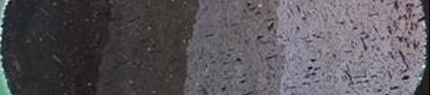


11 Initial Microstructure before ATC Slow Cooled SAC105 Fast Cooled SAC105 Fast Cooled SAC305 Slow Cooled SAC305 11/1/
12 Initial Microstructure before ATC FAST COOLED SLOW COOLED SAC305 The microstructure of the SAC305 solder joints exhibited hb Sn cells with regions of binary eutectic decomposition at their boundaries. The Sn cell size is larger with the slow cooling rate. SAC105 The microstructure of the SAC105 solder joints exhibited Sn cells with regions of binary eutectic decomposition at their boundaries. The Sn cell size is also larger with the slow cooling rate. 11/1/
13 Initial Microstructure of SAC105 before ATC FAST COOLED SLOW COOLED SAC105 In addition, the microstructure of the slow cooled SAC105 exhibited: Relatively more Cu 6 Sn 5 IMC particles Wider areaofbinary eutectic at the Sn boundaries Intermetallic spalling* *Spalling is the result of solidification conditions that t promote a quasi peritecticreaction it ti ti in Sn based solders in the presence of Cu and Ni [L. Snugovsky, Materials Science and Technology, vol. 25, no. 10, , (2009)]. 11/1/
14 Initial Microstructure of SAC305 before ATC FAST COOLED SLOW COOLED SAC305 The microstructure of the slow cooled SAC305 exhibited: Relatively more Cu 6 Sn 5 IMC particles Wider areaofbinary eutectic at the Sn boundaries 11/1/
15 Summary of Weibull Data for ATC Testing 11/1/
16 Weibull plot of ATC Testing Results Slow cooled SAC305 solder joints showed slightly ybetter fatigue resistance sta cethan SAC105 solder joints at 10 minute dwell time during ATC. There was virtually no difference in fatigue resistance between SAC305 and SAC105 solder joints at 60 minute dwell time during ATC. 11/1/
17 Weibull plot of ATC Testing Results For the eutectic Sn Pbsolder joints better fatigue resistance was observed with fast cooling at both 10 and 60 minute dwell times. However, the over all fatigue resistance was significantly lower for the solder joints tested at 60 minute dwell time during ATC. 11/1/


18 Failure mode and crack location SAC105 SLOW COOLED SAC305 SLOW COOLED The location of the first failure for all test cells was in the outer row of balls, at or near a corner position of the package. Failure mode was inter granular crack along Sn cell boundaries All samples exhibited the same failure mode SAC105 FAST COOLED SAC305 FAST COOLED 11/1/


19 Microstructure of SAC305 near failure site after ATC Testing FAST COOLED SLOW COOLED Backscattered electron images illustrating i the microstructural evolution in the SAC305 alloy. SAC305 11/1/


20 Microstructure of SAC105 near failure site after ATC Testing FAST COOLED SLOW COOLED Backscattered electron images illustrating the microstructural evolution in the SAC105 alloy. The intermetallic spalling did not appear to have an impact on fatigue crack propagation. SAC105 11/1/
21 Microstructure, Cooling Rate, Ag Composition & ATC Major Findings 1. Cooling rate was found to have little effect on the fatigue life of SAC solder joints. The fatigue life of SAC solder joints was not significantly affected by the range of cooling rate used in a typical PCB assembly reflow soldering process. 2. The fatigue life of SAC solder joints was not found to be affected by Ag content. At higher dwell time (60 minutes), the fatigue life of SAC305 and SAC105 were found to be nearly identical independent of cooling rate. 3. Longer dwell time during ATC testing dramatically reduced the fatigue life of the SAC105, SAC305 and Sn Pb (eutectic or near eutectic) solder joints. 4. Both SAC305 & SAC105 alloys exhibited slightly better fatigue resistance with slow cooling than fast cooling. 5. For the eutectic or near eutectic Sn Pb solder, fast cooled solder joints exhibited better fatigue resistance. 6. Both Pb free solders alloys show significantly higher fatigue resistance than eutectic SnPb solder. 11/1/
22 CONCLUSIONS I. Cooling rate and Ag composition were found to have no significant effect on the fatigue life of SAC solder joints. II. Magnitude of Stress, dwell time during ATC, was found to have a significant impact on fatigue life of solder joints. III. The fatigue life of SAC305 and SAC105 were found to be far more superior to that of the eutectic or near eutectic Sn Pb solder joints. 11/1/
23 ACKNOWLEDGEMENT This work was a joint project between R. Coyle from Alcatel-Lucent and M. Abtew and R. Kinyanjui from Sanmina-SCI. The work has been published in the SMTA proceedings, 2011 under the title Solder Joint Reliability of Pb-free Tin- Silver-Copper Ceramic Ball Grid Array (CBGA) Packages as a Function of Cooling Rate and Silver Content.
Composition/wt% Bal SA2 (SABI) Bal SA3 (SABI + Cu) Bal
 Bal SA3 (SABI + Cu) Bal") Improving Thermal Cycle and Mechanical Drop Impact Resistance of a Lead-free Tin-Silver-Bismuth-Indium Solder Alloy with Minor Doping of Copper Additive Takehiro Wada 1, Seiji Tsuchiya 1, Shantanu Joshi
Improving Thermal Cycle and Mechanical Drop Impact Resistance of a Lead-free Tin-Silver-Bismuth-Indium Solder Alloy with Minor Doping of Copper Additive Takehiro Wada 1, Seiji Tsuchiya 1, Shantanu Joshi
The Relationship between Backward Compatible Assembly and Microstructure on the Thermal Fatigue Reliability of an Extremely Large Ball Grid Array
 The Relationship between Backward Compatible Assembly and Microstructure on the Thermal Fatigue Reliability of an Extremely Large Ball Grid Array Richard Coyle, Richard Popowich, Peter Read, and Debra
System Level Effects on Solder Joint Reliability
 System Level Effects on Solder Joint Reliability Maxim Serebreni 2004 2010 Outline Thermo-mechanical Fatigue of solder interconnects Shear and tensile effects on Solder Fatigue Effect of Glass Style on
SOLDER JOINT RELIABILITY TEST SUMMARY
 Project Number: SJR Tracking Code: TC0623-SEAF-SJR-1059 Requested by: Jeremy Wooldridge Date: 05/20/2008 Product Rev: D (SEAF), C (SEAM) Part #: SEAF-50-5.0-S-10-2-A/ SEAM-50-2.0-S-10-2-A SEAF-50-6.5-S-10-1-A/
COMPONENT LEVEL RELIABILITY FOR HIGH TEMPERATURE POWER COMPUTING WITH SAC305 AND ALTERNATIVE HIGH RELIABILITY SOLDERS
 As originally published in the SMTA Proceedings. COMPONENT LEVEL RELIABILITY FOR HIGH TEMPERATURE POWER COMPUTING WITH SAC305 AND ALTERNATIVE HIGH RELIABILITY SOLDERS Thomas Sanders, Sivasubramanian Thirugnanasambandam
Impact of Intermetallic Growth on the Mechanical Strength of Pb-Free BGA Assemblies
 Impact of Intermetallic Growth on the Mechanical Strength of Pb-Free BGA Assemblies Patrick Roubaud, Grace Ng, Greg Henshall Hewlett Packard Ronald Bulwith, Robert Herber - Alpha Metals Swaminath Prasad,
INTERFLUX ELECTRONICS NV
 Reflow soldering temperature profiling Min : 30sec Max : 120sec Max : +4 C/sec Max : 250 C Min : 230 C Min: +0,5 C/sec Min : +1 C/sec Max : +3 C/sec Max : +1 C/sec Max : -6 C/sec Min : -2 C/sec Min : +1
New Pb-Free Solder Alloy for Demanding Applications. Presented by Karl Seelig, VP Technology, AIM
 New Pb-Free Solder Alloy for Demanding Applications Presented by Karl Seelig, VP Technology, AIM Why REL? The evolution and expansion of electronics into more harsh operating environments performing more
Thermo-Mechanical FEM Analysis of Lead Free and Lead Containing Solder for Flip Chip Applications
 Thermo-Mechanical FEM Analysis of Lead Free and Lead Containing Solder for Flip Chip Applications M. Gonzalez 1, B. Vandevelde 1, Jan Vanfleteren 2 and D. Manessis 3 1 IMEC, Kapeldreef 75, 3001, Leuven,
SCV Chapter, CPMT Society, IEEE September 14, Voids at Cu / Solder Interface and Their Effects on Solder Joint Reliability
 Voids at / Solder Interface and Their Effects on Solder Joint Reliability Zequn Mei, Mudasir Ahmad, Mason Hu, Gnyaneshwar Ramakrishna Manufacturing Technology Group Cisco Systems, Inc. Acknowledgement:
A New Approach for Early Detection of PCB Pad Cratering Failures
 A New Approach for Early Detection of PCB Pad Cratering Failures Anurag Bansal, Gnyaneshwar Ramakrishna and Kuo-Chuan Liu Cisco Systems, Inc., San Jose, CA anurbans@cisco.com Abstract Pad cratering refers
Reliability Screening of Lower Melting Point Pb-Free Alloys Containing Bi
 Reliability Screening of Lower Melting Point Pb-Free Alloys Containing Bi Joseph M. Juarez, Jr., Michael Robinson, Joel Heebink Honeywell AZ, US mike.robinson6@honeywell.com joseph.juarez@honeywell.com
IMPACT OF MICROVIA-IN-PAD DESIGN ON VOID FORMATION
 IMPACT OF MICROVIA-IN-PAD DESIGN ON VOID FORMATION Frank Grano, Felix Bruno Huntsville, AL Dana Korf, Eamon O Keeffe San Jose, CA Cheryl Kelley Salem, NH Joint Paper by Sanmina-SCI Corporation EMS, GTS
IMPACT OF COMPONENT TERMINAL FINISH ON THE RELIABILITY OF Pb-FREE SOLDER JOINTS
 IMPACT OF COMPONENT TERMINAL FINISH ON THE RELIABILITY OF Pb-FREE SOLDER JOINTS Gregory Henshall, Patrick Roubaud, Geary Chew Hewlett-Packard Co. Palo Alto, California greg_henshall@hp.com Swaminath Prasad,
Reflow Profiling: Time a bove Liquidus
 Reflow Profiling: Time a bove Liquidus AIM/David Suraski Despite much research and discussion on the subject of reflow profiling, many questions and a good deal of confusion still exist. What is clear
but T m (Sn0.62Pb0.38) = 183 C, so this is a common soldering alloy.
 = 183 C, so this is a common soldering alloy.") T m (Sn) = 232 C, T m (Pb) = 327 C but T m (Sn0.62Pb0.38) = 183 C, so this is a common soldering alloy. T m (Au) = 1064 C, T m (Si) = 2550 C but T m (Au0.97Si0.03) = 363 C, so thin layer of gold is used
T m (Sn) = 232 C, T m (Pb) = 327 C but T m (Sn0.62Pb0.38) = 183 C, so this is a common soldering alloy. T m (Au) = 1064 C, T m (Si) = 2550 C but T m (Au0.97Si0.03) = 363 C, so thin layer of gold is used
Sample Preparation for Mitigating Tin Whiskers in alternative Lead-Free Alloys
 As originally published in the IPC APEX EXPO Conference Proceedings. Sample Preparation for Mitigating Tin Whiskers in alternative Lead-Free Alloys Mehran Maalekian Karl Seelig, V.P. Technology Timothy
DEVELOPMENT OF LEAD-FREE ALLOYS WITH ULTRA-HIGH THERMO- MECHANICAL RELIABILITY
 As originally published in the SMTA Proceedings. DEVELOPMENT OF LEAD-FREE ALLOYS WITH ULTRA-HIGH THERMO- MECHANICAL RELIABILITY Pritha Choudhury, Ph.D., Morgana Ribas, Ph.D., Ranjit Pandher, Ph.D., Anil
Eliminating Wave Soldering with Low Melting Point Solder Paste ABSTRACT Process Cost Reduction INTRODUCTION
 Eliminating Wave Soldering with Low Melting Point Solder Paste Mitch Holtzer and Tuck Weng Mok Alpha, an Alent plc Company 109 Corporate Blvd., South Plainfield, NJ 07080 USA Email: mholtzer@alent.com;
Effects of SAC Alloy Copper Dissolution Rates on PTH Processes: Cost and performance justify use of certain alternatives to SAC305/405
 Effects of SAC Alloy Copper Dissolution Rates on PTH Processes: Cost and performance justify use of certain alternatives to SAC305/405 1 Craig Hamilton, Polina Snugovsky (Celestica) & Matthew Kelly (IBM)
IEEE TRANSACTIONS ON COMPONENTS, PACKAGING, AND MANUFACTURING TECHNOLOGY PART B, VOL. 20, NO. 1, FEBRUARY
 IEEE TRANSACTIONS ON COMPONENTS, PACKAGING, AND MANUFACTURING TECHNOLOGY PART B, VOL. 20, NO. 1, FEBRUARY 1997 87 Effect of Intermetallic Compounds on the Thermal Fatigue of Surface Mount Solder Joints
Component Palladium Lead Finish - Specification Approved by Executive Board 1997-xx-xx August 22 Version
 Component Palladium Lead Finish - Specification Approved by Executive Board 1997-xx-xx August 22 Version Appendices 1. User Commitment Form 2. Supplier Compliance Form Table of contents 1. Background 2.
Simulation of Embedded Components in PCB Environment and Verification of Board Reliability
 Simulation of Embedded Components in PCB Environment and Verification of Board Reliability J. Stahr, M. Morianz AT&S Leoben, Austria M. Brizoux, A. Grivon, W. Maia Thales Global Services Meudon-la-Forêt,
Influence of Thermal Cycling on the Microstructure and Shear Strength of Sn3.5Ag0.75Cu and Sn63Pb37 Solder Joints on Au/Ni Metallization
 68 J. Mater. Sci. Technol., Vol.23 No.1, 2007 Influence of Thermal Cycling on the Microstructure and Shear Strength of Sn3.5Ag0.75Cu and Sn63Pb37 Solder Joints on Au/Ni Metallization Hongtao CHEN 1,2),
THERMAL CYCLING RELIABILITY OF CHIP RESISTOR LEAD FREE SOLDER JOINTS
 THERMAL CYCLING RELIAILITY OF CHIP RESISTOR LEAD FREE SOLDER JOINTS Jeffrey C. Suhling, H. S. Gale, R. Wayne Johnson, M. Nokibul Islam, Tushar Shete, Pradeep Lall, Michael J. ozack, John L. Evans Center
Effects of Solder Reflow Conditions on the Assembly of Electronics Packaging and Printed Circuit Boards
 Effects of Solder Reflow Conditions on the Assembly of Electronics Packaging and Printed Circuit Boards Gregory K. Arslanian, Minfa Lin, Amy Wressell, Tom Mebrahtu, Victor Wang Air Products and Chemicals
Green Product. 2 nd level reliability of tin plated components. Dr. Marc Dittes CAT AIT PGP
 Green Product 2 nd level reliability of tin plated components Infineon Outline Experimental parameters Testboard, paste, components, T-cycling, Shear test Reflow profile SnPbAg Reflow profile SnAgCu Reliability
Effects of Bi Content on Mechanical Properties and Bump Interconnection Reliability of Sn-Ag Solder Alloys
 Effects of Bi Content on Mechanical Properties and Bump Interconnection Reliability of Sn-Ag Solder Kazuki Tateyama, Hiroshi Ubukata*, Yoji Yamaoka*, Kuniaki Takahashi*, Hiroshi Yamada** and Masayuki Saito
HALT Testing of Backward Soldered BGAs on a Military Product
 As originally published in the IPC APEX EXPO Conference Proceedings. HALT Testing of Backward Soldered BGAs on a Military Product B. Gumpert, B. Fox, L. Woody Lockheed Martin Ocala, FL Abstract The move
Balver Zinn Josef Jost GmbH & Co. KG SN100C : Micro alloyed lead free solder The Nickel effects
 Paolo Corviseri / Balver Zinn Techn. Department Certified IPC-A-610 Trainer (CIT) Paolo.corviseri@balverzinn.com Phone: +49 2375 1 915150 Mobil: +49 170 6379549 Balver Zinn Josef Jost GmbH & Co. KG SN100C
Low Cycle Fatigue Testing of Ball Grid Array Solder Joints under Mixed-Mode Loading Conditions
 Tae-Sang Park Mechatronics & Manufacturing Technology Center, Corporate Technology Operations, Samsung Electronics Co., LTD, 416, Maetan-3Dong, Yeongtong-Gu, Suwon-City, Gyeonggi-Do, 443-742, Korea e-mail:
THE EFFECTS OF PHOSPHORUS IN LEAD-FREE SOLDERS
 As originally published in the SMTA Proceedings. THE EFFECTS OF PHOSPHORUS IN LEAD-FREE SOLDERS Keith Sweatman, Takatoshi Nishimura and Takuro Fukami Nihon Superior Co., Ltd Osaka, Japan k.sweatman@nihonsuperior.co.jp
Reliability of Interconnects in LED Lighting Assemblies Utilizing Metal Clad Printed Circuit Boards Stefano Sciolè BDM I.M.S.
 Reliability of Interconnects in LED Lighting Assemblies Utilizing Metal Clad Printed Circuit Boards Stefano Sciolè BDM I.M.S. Henkel Electronic Materials Agenda 1. Introduction 2. Motivation 3. Interconnect
The hand soldering process can therefore be defined by the following steps ;
 Hand Soldering with Lead Free Alloys Introduction As companies start to implement lead free soldering processes, hand soldering and associated techniques have been identified as key functions in the manufacturing
Basic PCB Level Assembly Process Methodology for 3D Package-on-Package
 Basic PCB Level Assembly Process Methodology for 3D Package-on-Package Vern Solberg STC-Madison Madison, Wisconsin USA Abstract The motivation for developing higher density IC packaging continues to be
EPOXY FLUX MATERIAL AND PROCESS FOR ENHANCING ELECTRICAL INTERCONNECTIONS
 As originally published in the SMTA Proceedings. EPOXY FLUX MATERIAL AND PROCESS FOR ENHANCING ELECTRICAL INTERCONNECTIONS Neil Poole, Ph.D., Elvira Vasquez, and Brian J. Toleno, Ph.D. Henkel Electronic
CHAPTER 9 PHASE DIAGRAMS
 CHAPTER 9 PHASE DIAGRAMS PROBLEM SOLUTIONS 9.14 Determine the relative amounts (in terms of mass fractions) of the phases for the alloys and temperatures given in Problem 9.8. 9.8. This problem asks that
Correlations between IMC thickness and three factors in Sn-3Ag-0.5Cu alloy system
 Correlations between IMC thickness and three factors in Sn-3Ag-0.5Cu alloy system MENG Gong-ge( 孟工戈 ) 1, T. Takemoto 2, H. Nishikawa 2 1. College of Materials Science and Engineering, Harbin University
Discrete Capacitor & Resistor Issues. Anthony Primavera Boston Scientific CRM 11/13/06
 Discrete Capacitor & Resistor Issues Anthony Primavera Boston Scientific CRM 11/13/06 Goal: Drive the Industry towards common test methods and best practices in manufacturing to reduce and or eliminate
Becoming Lead Free. Automotive Electronics. Antonio Aires Soldering Technical Specialist Visteon Corporation - Palmela Plant
 Automotive Electronics Becoming Lead Free Antonio Aires Soldering Technical Specialist Visteon Corporation - Palmela Plant 1 Agenda 1. Leadfree Electronics Drivers 2. Requirements 3. Areas of Impact 4.
LEAD FREE ALLOY DEVELOPMENT
 LEAD FREE ALLOY DEVELOPMENT Karl F. Seelig, VP of Technology AIM Cranston, RI. USA. kseelig@aimsolder.com Abstract. When lead-free solders were first introduced to the electronics industry in the early
Validated Test Method to Characterize and Quantify Pad Cratering Under Bga Pads on Printed Circuit Boards
 Validated Test Method to Characterize and Quantify Pad Cratering Under Bga Pads on Printed Circuit Boards Mudasir Ahmad, Jennifer Burlingame, Cherif Guirguis Technology and Quality Group Cisco Systems,
3D-WLCSP Package Technology: Processing and Reliability Characterization
 3D-WLCSP Package Technology: Processing and Reliability Characterization, Paul N. Houston, Brian Lewis, Fei Xie, Ph.D., Zhaozhi Li, Ph.D.* ENGENT Inc. * Auburn University ENGENT, Inc. 2012 1 Outline Packaging
A STUDY OF THE ENEPIG IMC FOR EUTECTIC AND LF SOLDERS
 A STUDY OF THE ENEPIG IMC FOR EUTECTIC AND LF SOLDERS G.Milad, D.Gudeczauskas, G.Obrien, A.Gruenwald Uyemura International Corporation Southington, CT ABSTRACT: The solder joint formed on an ENEPIG surface
RoHS Compliance Document
 D2-Pak RoHS Compliance Document Contents: 1. 2. Solder Reflow 3. Tin Whisker Report D2-pak (3 or 5 Lead) BOM 1 90598-46-2 0.05808 11% 3.8% Lead Frame Copper 0.94840 Die Attach Soft Solder 0.01200 Cu 7440-50-8
Head-in-Pillow BGA Defects Karl Seelig AIM Cranston, Rhode Island, USA
 Head-in-Pillow BGA Defects Karl Seelig AIM Cranston, Rhode Island, USA Head-in-pillow (HiP), also known as ball-and-socket, is a solder joint defect where the solder paste deposit wets the pad, but does
Sample Preparation for Mitigating Tin Whiskers in alternative Lead-Free Alloys
 Sample Preparation for Mitigating Tin Whiskers in alternative Lead-Free Alloys Mehran Maalekian Karl Seelig, V.P. Technology Timothy O Neill, Technical Marketing Manager AIM Solder Cranston, RI Abstract
Low Temperature Lead-Free Production Versus SAC
 Low Temperature Lead-Free Production Versus SAC Designing a product that has minimal environmental impact for its entire life cycle is very demanding and a real challenge for designers and manufacturers.
Effect of Magnesium Addition on Microstructure and Mechanical Properties of Lead-Free Zinc-Silver Solder Alloys
 Effect of Magnesium Addition on Microstructure and Mechanical Properties of Lead-Free Zinc-Silver Solder Alloys Md. Anisul Islam * and Ahmed Sharif Department of Materials and Metallurgical Engineering,
CHAPTER 10 PHASE DIAGRAMS PROBLEM SOLUTIONS
 CHAPTER 10 PHASE DIAGRAMS PROBLEM SOLUTIONS Solubility Limit 10.1 Consider the sugar water phase diagram of Figure 10.1. (a) How much sugar will dissolve in 1000 g of water at 80 C (176 F)? (b) If the
Lead Free Assembly: A Practical Tool For Laminate Materials Selection
 Lead Free Assembly: A Practical Tool For Laminate Materials Selection Erik J. Bergum David Humby Isola Abstract: The impending European RoHS legislation, restricting the use of lead containing solders,
Lead-Free Solder Bump Technologies for Flip-Chip Packaging Applications
 Lead-Free Solder Bump Technologies for Flip-Chip Packaging Applications Zaheed S. Karim 1 and Jim Martin 2 1 Advanced Interconnect Technology Ltd. 1901 Sunley Centre, 9 Wing Yin Street, Tsuen Wan, Hong
SN100C Technical Guide
 SN100C Technical Guide INTRODUCTION SN100C is a lead-free tin/copper//germanium alloy. It has been in use since about the year 2000. Since then SN100C has become a world leading alloy in wave and selective
Packaging Technologies for SiC Power Modules
 Packaging Technologies for SiC Power Modules Masafumi Horio Yuji Iizuka Yoshinari Ikeda ABSTRACT Wide bandgap materials such as silicon carbide (SiC) and gallium nitride (GaN) are attracting attention
CHAPTER 9 PHASE DIAGRAMS PROBLEM SOLUTIONS
 CHAPTER 9 PHASE DIAGRAMS PROBLEM SOLUTIONS 9.17 A 90 wt% Ag-10 wt% Cu alloy is heated to a temperature within the β + liquid phase region. If the composition of the liquid phase is 85 wt% Ag, determine:
The Morphology Evolution and Voiding of Solder Joints on QFN Central Pads with a Ni/Au Finish
 The Morphology Evolution and Voiding of Solder Joints on QFN Central Pads with a Ni/Au Finish Julie Silk 1, Jianbiao Pan 2, Mike Powers 1 1 Agilent Technologies, 1400 Fountaingrove Parkway, Santa Rosa,
Manufacturing and Reliability Modelling
 Manufacturing and Reliability Modelling Silicon Chip C Bailey University of Greenwich London, England Printed Circuit Board Airflow Temperature Stress at end of Reflow Stress Product Performance in-service
PCB Technologies for LED Applications Application note
 PCB Technologies for LED Applications Application note Abstract This application note provides a general survey of the various available Printed Circuit Board (PCB) technologies for use in LED applications.
Rockwell R RF to IF Down Converter
 Construction Analysis Rockwell R6732-13 RF to IF Down Converter Report Number: SCA 9709-552 Global Semiconductor Industry the Serving Since 1964 17350 N. Hartford Drive Scottsdale, AZ 85255 Phone: 602-515-9780
THERMAL CYCLING RELIABILITY OF LEAD FREE SOLDERS
 THERMAL CYCLING RELIABILITY OF LEAD FREE SOLDERS FOR AUTOMOTIVE APPLICATIONS Jefsey C. Suhlmg, H. S. Gale, R. Wayne Johnson, M. Nokibul Islam, Tushar Shete, Pradeep Lall, Michael J. Bozack, John L. Evans
Low/No Silver Alloy Solder Paste
 Low/No Silver Alloy Solder Paste Definition Stage : Phase 1 Process Feasibility Study Project Leader: Jennifer Nguyen, Flextronics Project Facilitator: John Davignon HDP User Group Member Meeting Feb 26,
THIN IMMERSION TIN USING ORGANIC METALS
 THIN IMMERSION TIN USING ORGANIC METALS Jim Kenny, Nils Arendt, Bernhard Wessling, and Karl Wengenroth Enthone Inc., A Business of Cookson Electronics West Haven, CT, USA ABSTRACT With the international
Welcome to the Real World of Lead Free Soldering
 Welcome to the Real World of Lead Free Soldering Metallic Resources, Inc. Howard Stevens Nimal Liyanage,, Ph.D Objective: to Provide Education Regarding the Effects of Various Lead Free Soldering Alloys
Field Condition Reliability Assessment for SnPb and SnAgCu Solder Joints in Power Cycling Including Mini Cycles
 Field Condition Reliability Assessment for SnPb and SnAgCu Solder Joints in Power Cycling Including Mini Cycles Min Pei 1, Xuejun Fan 2 and Pardeep K. Bhatti 2 1 Georgia Tech, 801 Ferst Dr. NW, Atlanta,
Material Selection and Parameter Optimization for Reliable TMV Pop Assembly
 Selection and Parameter Optimization for Reliable TMV Pop Assembly Brian Roggeman, David Vicari Universal Instruments Corp. Binghamton, NY, USA Roggeman@uic.com Martin Anselm, Ph.D. - S09_02.doc Lee Smith,
Characterizing the Lead-Free Impact on PCB Pad Craters
 Characterizing the Lead-Free Impact on PCB Pad Craters Brian Roggeman and Wayne Jones Advanced Process Lab Universal Instruments Corp. Binghamton, NY 13902 Abstract Pad cratering in Printed Circuit Boards
WF6317. A superactive low-volatile/high heat-resistant water-soluble flux for ball soldering
 WF637 A superactive low-volatile/high heat-resistant water-soluble flux for ball soldering Low viscosity and high tacking power stabilize ball holding force and ensures excellent solder wettability Easy
Effects of Lead on Tin Whisker Elimination
 Effects of Lead on Tin Whisker Elimination Wan Zhang and Felix Schwager Rohm and Haas Electronic Materials Lucerne, Switzerland inemi Tin Whisker Workshop at ECTC 0 May 30, 2006, in San Diego, CA Efforts
A Solder Joint Reliability Model for the Philips Lumileds LUXEON Rebel LED Carrier Using Physics of Failure Methodology
 A Solder Joint Reliability Model for the Philips Lumileds LUXEON Rebel LED Carrier Using Physics of Failure Methodology Rudi Hechfellner 1, Michiel Kruger 1, Tewe Heemstra 2 Greg Caswell 3, Nathan Blattau
C β = W β = = = C β' W γ = = 0.22
 9-15 9.13 This problem asks us to determine the phases present and their concentrations at several temperatures, as an alloy of composition 52 wt% Zn-48 wt% Cu is cooled. From Figure 9.19: At 1000 C, a
Effect of Encapsulation Materials on Tensile Stress during Thermo-Mechanical Cycling of Pb-Free Solder Joints
 Effect of Encapsulation Materials on Tensile Stress during Thermo-Mechanical Cycling of Pb-Free Solder Joints Maxim Serebreni, Dr. Nathan Blattau, Dr. Gilad Sharon, Dr. Craig Hillman DfR Solutions Beltsville,
The Effect of Cu and Ni on the Structure and Properties of the IMC Formed by the Reaction of Liquid Sn-Cu Based Solders with Cu Substrate
 WDS'08 Proceedings of Contributed Papers, Part III, 220 224, 2008. ISBN 978-80-7378-067-8 MATFYZPRESS The Effect of Cu and Ni on the Structure and Properties of the IMC Formed by the Reaction of Liquid
contaminated, or if the location of the assembly house is well above sea level.
 VAPOR PHASE REFLOW S EFFECT ON SOLDER PASTE RESIDUE SURFACE INSULATION RESISTANCE Karen Tellefsen. Mitch Holtzer, Corne Hoppenbrouwers Alpha Assembly Solutions South Plainfield, NJ, USA Roald Gontrum SmartTech
White Paper Quality and Reliability Challenges for Package on Package. By Craig Hillman and Randy Kong
 White Paper Quality and Reliability Challenges for Package on Package By Craig Hillman and Randy Kong Background Semiconductor technology advances have been fulfilling Moore s law for many decades. However,
Impact of Stencil Foil Type on Solder Paste Transfer Efficiency for Laser Cut SMT Stencils Greg Smith
 Impact of Stencil Foil Type on Solder Paste Transfer Efficiency for Laser Cut SMT Stencils Greg Smith Manager of Stencil Technology gsmith@blueringstencils.com Originally published in the Proceedings of
Parametric Design and Reliability Analysis of Wire Interconnect Technology Wafer Level Packaging
 Y. T. Lin Graduate Assistant C. T. Peng Graduate Assistant K. N. Chiang Associate Professor e-mail: Knchiang@pme.nthu.edu.tw Dept. of Power Mechanical Engineering, National Tsing Hua University, HsinChu
Effects of Design, Structure and Material on Thermal-Mechanical Reliability of Large Array Wafer Level Packages
 Effects of Design, Structure and Material on Thermal-Mechanical Reliability of Large Array Wafer Level Packages Bhavesh Varia 1, Xuejun Fan 1, 2, Qiang Han 2 1 Department of Mechanical Engineering Lamar
The Effect of Voiding in Solder Interconnections Formed from Lead Free Solder Pastes with Alloys of Tin, Silver and Copper
 SOLDER PRODUCTS VALUE COUNCIL ASSOCIATION CONNECTING ELECTRONICS INDUSTRIES The Effect of Voiding in Solder Interconnections Formed from Lead Free Solder Pastes with Alloys of Tin, Silver and Copper A
CHAPTER 9 PHASE DIAGRAMS PROBLEM SOLUTIONS
 CHAPTER 9 PHASE DIAGRAMS PROBLEM SOLUTIONS Solubility Limit 9.1 Consider the sugar water phase diagram of Figure 9.1. (a) How much sugar will dissolve in 1500 g water at 90 C (194 F)? (b) If the saturated
IMPLEMENTATION OF A FULLY MOLDED FAN-OUT PACKAGING TECHNOLOGY
 IMPLEMENTATION OF A FULLY MOLDED FAN-OUT PACKAGING TECHNOLOGY B. Rogers, C. Scanlan, and T. Olson Deca Technologies, Inc. Tempe, AZ USA boyd.rogers@decatechnologies.com ABSTRACT Fan-Out Wafer-Level Packaging
Available online at ScienceDirect. Procedia Engineering 79 (2014 )
") Available online at www.sciencedirect.com ScienceDirect Procedia Engineering 79 (2014 ) 333 338 37th National Conference on Theoretical and Applied Mechanics (37th NCTAM 2013) & The 1st International Conference
Available online at www.sciencedirect.com ScienceDirect Procedia Engineering 79 (2014 ) 333 338 37th National Conference on Theoretical and Applied Mechanics (37th NCTAM 2013) & The 1st International Conference
The Failure Mechanism of Recrystallization Assisted Cracking of Solder Interconnections
 The Failure Mechanism of Recrystallization Assisted Cracking of Solder Interconnections 8 Toni T. Mattila and Jorma K. Kivilahti Aalto University Finland 1. Introduction The typical user environment load
Effects of Flux and Reflow Parameters on Lead-Free Flip Chip Assembly. Sandeep Tonapi 1 Doctoral Candidate
 Effects of Flux and Reflow Parameters on Lead-Free Flip Chip Assembly Sandeep Tonapi 1 Doctoral Candidate Peter Borgesen, Ph.D. 2 Manager, Area Array Consortium K. Srihari, Ph.D. 1 Professor, Department
The role of minor modifying additives on soldering properties of Sn-Ag-Cu green solders
 Southern Cross University epublications@scu 23rd Australasian Conference on the Mechanics of Structures and Materials 2014 The role of minor modifying additives on soldering properties of Sn-Ag-Cu green
Chapter 10: Phase Diagrams
 hapter 10: Phase Diagrams Show figures 10-1 and 10-3, and discuss the difference between a component and a phase. A component is a distinct chemical entity, such as u, Ni, NiO or MgO. A phase is a chemically
An Innovative High Throughput Thermal Compression Bonding Process
 An Innovative High Throughput Thermal Compression Bonding Process Li Ming 2 September 2015 Outline Introduction Throughput improved TCB Process Liquid Phase Contact (LPC) bonding Flux-LPC-TCB under inert
Statement of Work (SOW) inemi Board Assembly TIG BiSn-Based Low-Temperature Soldering Process and Reliability Project
 inemi Board Assembly TIG BiSn-Based Low-Temperature Soldering Process and Reliability Project") Statement of Work (SOW) inemi Board Assembly TIG BiSn-Based Low-Temperature Soldering Process and Reliability Project Version 1.4 Date: December 1, 2015 Project Leader: Raiyo Aspandiar, Intel Corporation
Statement of Work (SOW) inemi Board Assembly TIG BiSn-Based Low-Temperature Soldering Process and Reliability Project Version 1.4 Date: December 1, 2015 Project Leader: Raiyo Aspandiar, Intel Corporation
Carol Handwerker NIST Gaithersburg MD October 20, 2003 IPC-Frankfurt
 NEMI Pb-Free Solder Projects: Progress and Results Carol Handwerker NIST Gaithersburg MD October 20, 2003 IPC-Frankfurt Outline History of Pb-Free Projects Worldwide and NEMI Project Structure Analysis
Failure Modes in Wire bonded and Flip Chip Packages
 Failure Modes in Wire bonded and Flip Chip Packages Mumtaz Y. Bora Peregrine Semiconductor San Diego, Ca. 92121 mbora@psemi.com Abstract The growth of portable and wireless products is driving the miniaturization
An Investigation of Reliability of High Density Electronic Package-to-Board Interconnections from the Perspective of Solder Joint Metallurgy
 Aalto University School of Science and Technology Faculty of Electronics, Communications and Automation Department of Electronics, Electronics Integration and Reliability Espoo, Finland, 2010 HUT-EPT-14
Reference Only. 2.Part Numbering (ex) NF Z 5B BW 2R9 L N 1 0 L
 NF Z 5B BW 2R9 L N 1 0 L") SpecNo.JENF243J-0011A-01 P1/10 CHIP NOISE FILTER NFZ5BBW LN10 REFERENCE SPECIFICATION 1.Scope This reference specification applies to NFZ5BBW_LN10L Series, Chip Noise Filter. 2.Part Numbering (ex) NF Z
SpecNo.JENF243J-0011A-01 P1/10 CHIP NOISE FILTER NFZ5BBW LN10 REFERENCE SPECIFICATION 1.Scope This reference specification applies to NFZ5BBW_LN10L Series, Chip Noise Filter. 2.Part Numbering (ex) NF Z
Dissolution of electroless Ni metallization by lead-free solder alloys
 Journal of Alloys and Compounds 388 (2005) 75 82 Dissolution of electroless Ni metallization by lead-free solder alloys Ahmed Sharif, Y.C. Chan, M.N. Islam, M.J. Rizvi Department of Electronic Engineering,
Ceramic Column Grid Array Design and Manufacturing Rules for Flight Hardware
 GODDARD TECHNICAL STANDARD GSFC-STD-6001 Goddard Space Flight Center Approved: 02-22-2011 Greenbelt, MD 20771 Expiration Date: 02-22-2016 Superseding GSFC-STD-XXXXR Ceramic Column Grid Array Design and
Board Level Reliability Improvement in ewlb (Embedded Wafer Level BGA) Packages
 Packages") Board Level Reliability Improvement in ewlb (Embedded Wafer Level BGA) Packages by Seng Guan Chow, Yaojian Lin, Bernard Adams * and Seung Wook Yoon** STATS ChipPAC Ltd. 5 Yishun Street 23, Singapore 768442
Board Level Reliability Improvement in ewlb (Embedded Wafer Level BGA) Packages by Seng Guan Chow, Yaojian Lin, Bernard Adams * and Seung Wook Yoon** STATS ChipPAC Ltd. 5 Yishun Street 23, Singapore 768442
Thermal and mechanical reliability tests of plastic core solder balls
 Thermal and mechanical reliability tests of plastic core solder balls Author: Maaike M. V. Taklo Company: SINTEF Email: mvi@sintef.no WS on 3D SiP, ESREF 2012 Cagliari, Italy, October 1st, 2012 Page 1
Metals I. Anne Mertens
 "MECA0139-1: Techniques "MECA0462-2 additives : et Materials 3D printing", Selection", ULg, 19/09/2017 25/10/2016 Metals I Anne Mertens Introduction Outline Metallic materials Materials Selection: case
Copyright 2009 Year IEEE. Reprinted from 2009 Electronic Components and Technology Conference. Such permission of the IEEE does not in any way imply
 Copyright 2009 Year IEEE. Reprinted from 2009 Electronic Components and Technology Conference. Such permission of the IEEE does not in any way imply IEEE endorsement of any of Institute of Microelectronics
726 IEEE TRANSACTIONS ON COMPONENTS, PACKAGING AND MANUFACTURING TECHNOLOGY, VOL. 7, NO. 5, MAY 2017
 726 IEEE TRANSACTIONS ON COMPONENTS, PACKAGING AND MANUFACTURING TECHNOLOGY, VOL. 7, NO. 5, MAY 2017 Board-Level Thermal Cycling and Drop-Test Reliability of Large, Ultrathin Glass BGA Packages for Smart
YOUR Strategic TESTING ENGINEERING CONCEPT SMT FLIP CHIP PRODUCTION OPTO PACKAGING PROCESS DEVELOPMENT CHIP ON BOARD SUPPLY CHAIN MANAGEMENT
 YOUR Strategic TECHNOLOGY PARTNER Wafer Back-End OPTO PACKAGING PROCESS DEVELOPMENT CONCEPT FLIP CHIP PROTOTYping ENGINEERING TESTING SMT PRODUCTION CHIP ON BOARD SUPPLY CHAIN MANAGEMENT Next Level 0f
Advanced Analytical Techniques for Semiconductor Assembly Materials and Processes. Jason Chou and Sze Pei Lim Indium Corporation
 Advanced Analytical Techniques for Semiconductor Assembly Materials and Processes Jason Chou and Sze Pei Lim Indium Corporation Agenda Company introduction Semiconductor assembly roadmap challenges Fine