AP 5301/8301 Instrumental Methods of Analysis and Laboratory Lecture 4 Microscopy (III): Transmission Electron Microscopy (TEM)
|
|
|
- Damian Bradley
- 5 years ago
- Views:
Transcription
1 1 AP 5301/8301 Instrumental Methods of Analysis and Laboratory Lecture 4 Microscopy (III): Transmission Electron Microscopy (TEM) Prof YU Kin Man kinmanyu@cityu.edu.hk Tel: Office: P6422
2 Lecture 4: Outline Introduction: Development of transmission electron microscope Essential parts and functions Operation principles TEM specimen preparation Imaging modes: brief field, dark field and high resolution TEM diffraction Diffraction basics TEM diffraction patterns Selected area electron diffraction Convergent beam electron diffraction Scanning transmission electron microscopy (STEM) Z-contrast imaging Electron probe microanalysis Electron energy loss spectroscopy Energy dispersive and wavelength dispersive x-ray spectroscopy 2
3 Optical and electron microscopes 3 Light source Condenser Specimen Source of electrons Magnetic lenses Objective Eyepiece Projector Specimen CRT Cathode Ray Tube detector OM TEM SEM


4 Transmission electron microscope 4
5 TEM: an introduction A short history: 1897 J. J. Thompson Discovers the electron 1924 Louis de Broglie: identifies the wavelength for electrons as λ = h/mv 1926 H. Busch: magnetic or electric fields act as lenses for electrons 1929 E. Ruska: Ph.D thesis on magnetic lenses 1931 Knoll & Ruska: built the 1st electron microscope (EM) 1931 Davisson & Calbrick: properties of electrostatic lenses 1934 Driest & Muller: surpass resolution of the Light Microscope 1938 von Borries & Ruska: first practical EM (Siemens) - 10 nm resolution 1940 RCA: commercial EM with 2.4 nm resolution 2000 new developments, cryomicroscopes, primary energies up to 1 MeV 5 Electrons at 300 kev have a λ~2 pm and a diffraction limited resolution ~1 pm In practice TEM resolution is far from these limits Imperfections (aberrations) of magnetic lenses are the limiting factor E (kev) Wavelength (pm)
6 Comparison: SEM and TEM 6 TEM SEM Electron beam Broad, static beam Beam focused to fine point and scan over specimen Electron path passes through thin specimen. scans over surface of specimen Specimens Specially prepared thin specimens supported on TEM grids. Sample can be any thickness and is mounted on an aluminum stub. Specimen stage Located halfway down column. At the bottom of the column. Image formation Transmitted electrons collectively focused by the objective lens and magnified to create a real image Image display On fluorescent screen. On TV monitor. Image nature Image is a two dimensional projection of the sample. Magnification Up to 5,000,000x ~250,000x Resolution ~0.2 nm ~2-5 nm Beam is scanned along the surface of the specimen to build up the image Image is of the surface of the sample
7 TEM: advantages and disadvantages Advantages TEMs offer very powerful magnification and resolution. TEMs have a wide-range of applications and can be utilized in a variety of different scientific, educational and industrial fields TEMs provide information on element and compound structure. Images are high-quality and detailed. Chemical information with analytical attachments 7 Disadvantages TEMs are large and very expensive (USD 300K to >1M) Laborious sample preparation. Operation and analysis requires special training. Samples are limited to small size (mm) and must be electron transparent. TEMs require special housing and maintenance. Images are black and white.
 are its high lateral spatial resolution (better than 0.")

, bonding (distance and")
8 Transmission electron microscopy (TEM) Two unique features of transmission electron microscopy (TEM) are its high lateral spatial resolution (better than 0.2 nm) and its capability to provide both image and diffraction information from a single sample. Hence TEM can be used to obtain full morphological, crystallographic, atomic structural and microanalytical such as chemical composition (at nm scale), bonding (distance and angle), electronic structure, coordination number data from the sample. 8 Diffraction Imaging Spectroscopy

9 TEM: operation principle Primary electrons generated by electron gun and focused by stages of condenser lenses into bundles Electrons illuminate the sample: at low magnification, a spread beam is used to illuminate a large area at high magnification, a strongly condensed beam is used The pattern of electrons leaving the object, reaches the objective lens forms the image. The image is greatly enlarged by a projector lens. The traversing electrons (transmission) reach the scintillator plate at the base of the column of the microscope. The scintillator contains phosphor compounds that can absorb the energy of the striking electrons and convert it to light flashes, forming an image 9


10 TEM: operation principle 10 A disc of metal Control brightness, convergence Control contrast
 Electron Gun")


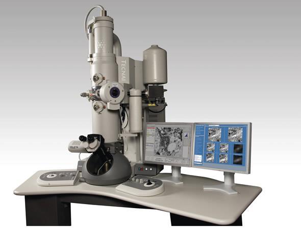
11 TEM: essential parts and functions Column CM200 (200kV) Electron Gun EDS Detector 11 Condenser Lens Objective Lens SAD Aperture Magnifying Lenses Binocular Fluorescenc e screen LN 2 Specimen Holder Cost: $4,000,000


12 Specimen Holder beam Rotation, tilting, heating, cooling and straining holder a split polepiece objective lens Double tilt heating Twin specimen holder Heating and straining


13 TEM: specimen preparation TEM is a microscopy technique whereby a beam of electrons is transmitted through an ultrathin specimen, interacting with the specimen as it passes through it. Materials for TEM must be specially prepared to thicknesses which allow electrons to transmit through the sample (~ nm). In addition to be thin, samples have to be: Electrically conductive Stable under vacuum Free from hydrocarbon contaminants No artefacts 13 For nanoparticles or thin foils, e.g. graphene, disperse crystals or powders on a carbon film on a Cu grid Thin foil


14 TEM: specimen preparation 14 For solid samples, there are different methods: Mechanical: Mechanical polishing down to electron transparency Cleavage Ultramicrotomy-using a (diamond) knife blade Crushing Mechanical+ionic/chemical Grinding, dimpling, ion milling Using kev Ar ions focused on the sample to thin it down Focused ion beam (FIB) Electro-chemical polishing Chemical polishing or etching ion milling Focused ion beam (FIB)


15 TEM: Cross-section specimen preparation 15 Cross sectional TEM: characterization of multilayer materials layers thickness measurement layers and interfaces structure analysis Cross-sectional TEM image of a silicatetitanate film containing 10 nm gold particles ess/case_example_49.html


16 TEM operation TEM offers two methods of specimen observation, diffraction mode and image mode. The objective lens forms a diffraction pattern in the back focal plane with electrons scattered by the sample and combines them to generate an image in the image plane. Whether the diffraction pattern or the image appears on the viewing screen depends on the strength of the intermediate lens. The diffraction pattern is entirely equivalent to an X-ray diffraction pattern. The image mode produces an image of the illuminated sample area In image mode, the post-specimen lenses are set to examine the information in the transmitted signal at the image plane of the objective lens. There are three primary image modes that are used in conventional TEM work, brightfield microscopy, dark-field microscopy, and high-resolution electron microscopy. 16
17 Use of apertures Condenser aperture: Limit the beam divergence (reducing the diameter of the discs in the convergent electron diffraction pattern). Limit the number of electrons hitting the sample (reducing the intensity) Objective aperture: Control the contrast in the image. Allow certain reflections to contribute to the image. Bright field imaging (central beam, 000), Dark field imaging (one reflection, g), High resolution Images (several reflections from a zone axis). Selected area aperture: Select diffraction patterns from small (> 1µm) areas of the specimen. Allows only electrons going through an area on the sample that is limited by the SAD aperture to contribute to the diffraction pattern (SAD pattern).
.")

18 TEM imaging: bright field In image mode, the post-specimen lenses are set to examine the information in the transmitted signal at the image plane of the objective lens. The scattered electron waves finally recombine, forming an image with recognizable details related to the sample microstructure (or atomic structure). There are three primary image modes: Bright field (BF): a small objective aperture is used to block all diffracted beams and to pass only the transmitted (undiffracted) electron beam. Contrast arises in a bright-field image when thickness or compositional variations or structural anomalies are present. Regions in which intensity is scattered (defects) appear dark High-Z material appear darker than the low-z material In crystalline materials, dark contrast regions in bright-field usually originate from areas that are aligned for Bragg diffraction TEM BF image of microcrystalline ZrO2. some crystals appear with dark contrast since they are oriented (almost) parallel to a zone axis (Bragg contrast). 18


, some of the microcrystals appear with bright")
 Bright-field (BF) micrograph of multilayer cross-section")
19 TEM imaging: dark field Dark field (DF): a small objective aperture is used to select a diffracted beam and block all other beams. Undistorted crystal lattice appears dark since little scattered intensity arises from these regions to contribute brightness. dislocations (defects) appear as bright lines on a dark background 19 In the DF image (right), some of the microcrystals appear with bright contrast, namely such whose diffracted beams partly pass the objective aperture (a) Bright-field (BF) micrograph of multilayer cross-section sample Ni/Co multilayera; (b) Dark-field (DF) TEM image.


20 TEM imaging: high resolution Phase contrast or high resolution (HREM): use the non-diffracted and at least one diffracted beams by using a large (or none) objective aperture and add them back together, phase and intensity to form an image When viewed at high-magnification, it is possible to see contrast in the image in the form of periodic fringes that represent direct resolution of the Bragg diffracting planes The contrast is referred to as phase contrast 20 Si D T BN Objective aperture High resolution TEM image of a RuO2 nanorod High Resolution Transmission Electron Microscope (HRTEM) Image of a Grain Boundary Film in Strontium-Titinate Electron diffraction pattern recorded from both BN film on Si substrate.
, the scattering event can be described as a reflection of the beams at planes of atoms (lattice planes) There are however fundamental")

21 TEM diffraction 21 Electrons like X-rays are scattered by atoms and can be used to analyze crystal structures in a similar way. As in X-ray diffraction (XRD), the scattering event can be described as a reflection of the beams at planes of atoms (lattice planes) There are however fundamental differences: Electrons have a much shorter wavelength than the X-rays X-rays are scattered by the electrons that make up the bulk of the atom. Electrons are charged particles and interact with the electrons surrounding atoms and also the nucleus. The elastic cross section of the electron is ca times larger than that of X-rays. Electron beams can be focused using electromagnetic lenses
 A wide range of θ hkl electrons λ = 0.037A (100kV) θ = 0.")
![26 o for d = 4A [001] Real lattice sample r L r = sin 2θ 2θ hkl For electrons: λ nm = For electron diffraction, the incident beam has to be](/docs-images/82/86096349/images/22-1.jpg "almost parallel to the planes for diffraction to occur, so that λ = 2d hkl θ hkl r L = λ d r = λl 1 d L is the camera length (mm) r is the")
22 TEM: electron diffraction e - Bragg s law: λ = 2d hkl sin θ hkl 22 d hkl e-beam Zone axis of crystal L 2 Specimen foil x-ray λ = 1.54A (Cu K) A wide range of θ hkl electrons λ = 0.037A (100kV) θ = 0.26 o for d = 4A [001] Real lattice sample r L r = sin 2θ 2θ hkl For electrons: λ nm = For electron diffraction, the incident beam has to be almost parallel to the planes for diffraction to occur, so that λ = 2d hkl θ hkl r L = λ d r = λl 1 d L is the camera length (mm) r is the distance between T and D spots 1/d is the reciprocal of interplanar distance (A 1 ) 1.5 V+10 6 V 2
23 Reciprocal lattice Reciprocal lattice is another way to view a crystal lattice and is used to understand diffraction patterns. A dimension of 1/d (Å -1 ) is used in reciprocal lattices. g reciprocal lattice vector 23

24 TEM: diffraction intensity 24 + lattice basis Spot (ring) intensity: I hkl F hkl 2 Crystal structure Structure Factor: F hkl = basis f j exp 2πi(hu j + kv j + lw j ) where f j is the atomic scattering factor, and is dependent on atomic number u j,v j, w j are the fractional distances within the unit cell h, k, l is the Miller indices of the plane Atomic scattering factor: λ f θ sin θ Z 2 where Z is the atomic number of the atom
![TEM: structure factor (example) 25 We can consider the BCC structure as a simple cubic lattice with a two atom basis, with atoms at [000] and [½½½] F hkl = basis f j exp 2πi(hu j + kv j + lw j ) F](/docs-images/82/86096349/images/25-0.jpg "hkl = fexp i0 + fexp 2πi( 1 2 h + 1 2 k + 1 2 l) ( 1 2 1 2 1 2) F hkl = f 1 + exp iπ(h + k + l) (000) Hence: F hkl = 2f if h + k + l is even 0 if h + k + l is odd For a monatomic BCC crystal")
25 TEM: structure factor (example) 25 We can consider the BCC structure as a simple cubic lattice with a two atom basis, with atoms at [000] and [½½½] F hkl = basis f j exp 2πi(hu j + kv j + lw j ) F hkl = fexp i0 + fexp 2πi( 1 2 h k l) ( ) F hkl = f 1 + exp iπ(h + k + l) (000) Hence: F hkl = 2f if h + k + l is even 0 if h + k + l is odd For a monatomic BCC crystal diffraction from (111), (003), (201), (221), etc. are missing and these are the forbidden diffractions


 in the direction of the normal to")
26 TEM: diffraction pattern 26 (010) (100) For a simple cubic structure a d hkl = h 2 + k 2 + l θ T r 010 Real lattice T r D reciprocal lattice r hkl = Lλ/d hkl Diffraction pattern: points with space distance proportional to the reciprocal of the interplanar spacing (1/d) in the direction of the normal to the plane

 Polycrystalline nickel mono silicide (NiSi) on top of")
 the rings get more diffuse")
27 TEM: diffraction pattern Polycrystalline materials The electron diffraction pattern is a set of rings, with some spots depending on the crystallite sizes. 27 Al single crystal Polycrystalline Pt silicide (PtSi) Silicon with epitaxial nickel silicides ( Si - NiSi - NiSi 2 ) Polycrystalline nickel mono silicide (NiSi) on top of single crystalline silicon (Si). Nano to Amorphous materials As the crystal size get smaller (nm) the rings get more diffuse and eventually become halo-like when the material becomes amorphous nanocrystalline GaNAs Amorphous GaNAs


28 TEM: selected area electron diffraction (SAED) Selected Area Electron Diffraction SAED is probably the most commonly used TEM technique. A selected area aperture is located underneath the sample holder and can be adjusted to block parts of the beam so as to examine just selected areas of the sample. Combined with sample tilting, diffraction images of single crystallites can be obtained in various orientations. Single crystals of a few hundred nm in size can be examined in this way. 28


29 TEM: diffraction pattern Each grain is a single crystal 29 A single grain Another grain (different orientation) Two grains More grains Many grains SAED aperture Many grains covered by SAED aperture

")

30 TEM: convergent beam electron diffraction 30 Parallel beam (SAED) Convergent beam (CBED) Convergence angle Spatial resolution beam size T D disks [hkl]


![CBED patterns of a Cu2ZnSnS4 crystal in the [010] orientation disc and line patterns packed with information CBED patterns contain a wealth](/docs-images/82/86096349/images/31-2.jpg "of information about symmetry and thickness of specimen.")
31 TEM: convergent beam electron diffraction 31 Convergent Beam Electron Diffraction (CBED): converging the electrons in a cone onto the specimen, one can in effect perform a diffraction experiment over several incident angles simultaneously. This technique can reveal the full threedimensional symmetry of the crystal. Each spot in SAED then becomes a disk within which variations in intensity can be seen. CBED patterns of a Cu2ZnSnS4 crystal in the [010] orientation disc and line patterns packed with information CBED patterns contain a wealth of information about symmetry and thickness of specimen. The information is generated from small regions beyond reach of other techniques (<1 nm) Applications: Phase identification Symmetry determination Phase fingerprinting Thickness measurement Strain and lattice parameter Structure factor


32 TEM: convergent beam electron diffraction 32 The convergence semiangle, α, can be adjusted by changing the C2 aperture. The size of the diffraction disk depends on α. Depending on α different patterns are produced. Electrons are scattered in all directions in the convergent conical illumination. Each point in the disc can be scattered by the same 2θ. Therefore the diffracted electrons also form discs, one for each Bragg reflection. Weaknesses: Limited to crystalline specimens Complicated analysis, normally compared to computer simulated pattern. The focused beam gives a very high current density which causes damage to the sample. Specimens are typically cooled with LN 2

 m")
33 33 CBED: phase identification in BaAl 2 Si 2 O 8 Hexagonal Orthorhombic Hexagonal m m 6mm 2mm 6mm 200 o C 400 o C 800 o C <0001> CBED (top) and SAED (bottom) patterns 6 - rotation axis (rotation about axis by 360/6 degrees) m mirror plane


34 Scanning Transmission Electron Microscopy (STEM) 34 In a STEM the electron beam is focused into a narrow spot which is scanned over the sample in a rastering mode. With STEM we can use many more of these signals in a highly spatially resolved way than we can with TEM SEM EDS EELS CL Z-contrast image
 spectroscopy electron energy loss")
35 Scanning Transmission Electron Microscopy (STEM) 35 EDX detector X-rays luminescence I Z 2 SAED =0.26 o or ~6.4 mrads The rastering of the beam across the sample makes these microscopes suitable for analysis techniques such as mapping by energy dispersive X-ray (EDX) spectroscopy electron energy loss spectroscopy (EELS) annular dark-field imaging (ADF). By using a high-angle detector (high angle annular dark-field HAADF), atomic resolution images where the contrast is directly related to the atomic number (z-contrast image) can be formed.
 Z 2 Rutherford scattering will dominate when the")

36 STEM: Z-contrast imaging 36 Low angle scattering: Coulombic interaction with the electron cloud Higher angle scattering: Coulombic interaction with the nucleus Rutherford scattering with cross section σ R σ R (θ) Z 2 Rutherford scattering will dominate when the scattering angle > screening parameter θ o θ o = 0.117Z1/3 E o 1/2, E o in kev e.g. Cu for 200 kev e-beam, θ o 25 mrad Z-sensitive electrons can be collected by using a detector/camera length combination that gives large collection angles (e.g. β > mrad): high-angle annular darkfield (HAADF)


")

37 STEM: HAADF images 37 STEM HAADF micrographs of 2 layers of Bi absorbed along the general GBs of a Ni polycrystal quenched from 700 o C SrTiO 3 detail/jem-2800.html (a) HRTEM and (b) HAADF-STEM images of Pt nanoparticles (diameter 1-2 nm) dispersed on ceria. Krumeich and Müller HREM-TEM HR Z-contrast STEM Pt pn TiO 2 Pt on C foil


38 Electron probe microanalysis (EPMA) 38 Electron energy loss spectroscopy (EELS) Electrons lose energy through inner-shell ionizations are useful for detecting the elemental components of a material. In Electron Energy Loss Spectroscopy (EELS) characteristic spectral signature, termed the edge profile, is derived from the excitation of discrete inner shell levels to empty states above the Fermi level. By studying the detailed shape of the spectral profiles measured in EELS, the electronic structure, chemical bonding, and average nearest neighbor distances for each atomic species detected can be derived. Quantitative elemental concentration determinations can be obtained for the elements 3 Z 35 using a standard-less data analysis procedure

39 EPMA: electron energy loss process Measures the changes in the energy distribution of an electron beam transmitted through a thin specimen. The energy loss process is the primary interaction event. All other sources of analytical information ( i.e. X-rays, Auger electrons, etc.) are secondary products of the initial inelastic event. 39
40 EPMA: EELS spectrum 40 Region 1: zero loss peak, represents electrons that have passed through the specimen suffering either negligible or no energy losses Region 2 (~1-50 ev): low loss regime, exhibits a series of broad spectral features related to inelastic scattering with the valence electron structure of the material. In metallic systems these peaks arise due to a collective excitation of the valence electrons, and are termed plasmon oscillations or peaks Region 3 (extending to ev): a series of edges resulting from electrons that have lost energy corresponding to the creation of vacancies in the deeper core levels of the atom (K, L, M shells). Edge energies are characteristic for each element and therefore can identify different elements and their quantity (edge height).
 based on the size and the shape of nanotube.")
41 EPMA: EELS elemental mapping 41 a) HREM image of a carbon nanotube. b) Carbon map at the same region. c) EELS spectrum d) Intensity profile of carbon map perpendicular to the tube axis. The intensity profile corresponds well to the calculated number distribution of carbon atom (solid line) based on the size and the shape of nanotube. The intensity dip at center part corresponds to 20 carbon atoms.

42 EPMA: EELS spectrum 42 The inner shell edge profile in EELS varies with the edge type (K, L, M, etc.), the electronic structure, and the chemical bonding. The details of the profile is a measure of the empty local density of states above the Fermi level of the elemental species being studied. For example, Carbon edge from graphite, C60 and diamond show very different fine structures. Comparing spectra with data library or computation can reveals the bonding state and local electronic structure of the particular sample.
 in a PtFe nanowire Zhu et al.")
 Mn L2,3-edges elemental map; e) colorized map using the color scheme from")
43 EELS: examples 43 SrTiO3/SrLaMnO3 interface Ti La Sr Mn Two-dimensional EELS elemental mapping of Fe (red) and Pt (green) in a PtFe nanowire Zhu et al. JACS, 137 (32 (2015) SrTiO 3 SrLaMnO 3 a) Ti L2,3-edges elemental map; b) La M4,5-edges elemental map; c) Sr L2,3-edges at 1940 ev elemental map; d) Mn L2,3-edges elemental map; e) colorized map using the color scheme from Figures 9a-d.
, is an analytical technique used for the elemental analysis or chemical characterization of a sample. It relies on an interaction of some source of X-ray excitation and a sample.")
44 EPMA: Energy dispersive x-ray spectroscopy 44 Energy-dispersive X-ray spectroscopy (EDS, EDX, or XEDS), sometimes called energy dispersive X-ray analysis (EDXA) or energy dispersive X-ray microanalysis (EDXMA), is an analytical technique used for the elemental analysis or chemical characterization of a sample. It relies on an interaction of some source of X-ray excitation and a sample. A high-energy beam of charged particles such as electrons or protons (PIXE), or a beam of X-rays (XRF), is focused into the sample. The incident beam excites an electron in an inner shell, ejecting it from the shell while creating an electron hole. An electron from an outer shell fills the hole, and the difference in energy between the two shells may be released in the form of an X-ray. The emitted x-rays are characteristic to specific elements and can be measured by an energy-dispersive spectrometer giving information on the identity and amount of the atoms in the sample.
 create a depletion width larger than the x-ray penetration depth (mm).")
45 EDS detectors: Si(Li), Ge(Li) 45 A ED-spectrometer is p-n junction (or Schottky) of a high purity Si or Ge semiconductor crystal (typically compensated with Li). A high negative voltage is applied over the crystal ( V) create a depletion width larger than the x-ray penetration depth (mm). When x-rays enter the crystal electron-hole pairs are formed and the number is proportional to the energy of the x-ray. The e h pairs are swept across the semiconductor creating a current pulse with an amplitude proportional to the energy. The crystal is cooled (using a LN2 dewar or thermal-electric cooled) to reduce thermal excitation (noise). Measuring the amplitude and counting produces the ED-spectrum. Energy resolution ~ ev


46 EDS: characteristic x-rays 46 Characteristic x-ray line energy= E final E initial Relative intensities of major x-ray lines K α1 = 100 L α1 = 100 M α1,2 = 100 K α2 = 50 L α2 = 50 M β = 60 K β1 = L β1 = 50 K β2 = 1 10 L β2 = 250 K β3 = 6 15 L β3 = 1 6 L β4 = 3 5 L γ1 = 1 10

47 EDS: in SEM/TEM/STEM 47
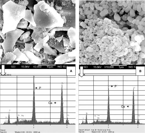
 microanalysis for calcium oxalate (CaOx) crystals. Chen et al. Kidney intnl. 80, 369 (2011)")
48 SEM-EDS analysis: example 48 Scanning electron microscopy (SEM) and energy-dispersive X-ray spectroscopy (EDS or EDX) microanalysis for calcium oxalate (CaOx) crystals. Chen et al. Kidney intnl. 80, 369 (2011)

49 SEM-EDS elemental mapping 49 Fe 3 O 4 /graphene prepared at a low concentration of Fe 2+ ions Lim et al., in Advanced Topics on Crystal Growth, Chapter 12 (2013) ISBN


50 EDS vs EELS mapping 50 EELS / EDS color map of a SrTiO3 crystal Fast joint EELS / EDS color map across a 32 nm transistor device


51 Wavelength dispersive x-ray spectroscopy Wavelength-dispersive X-ray spectroscopy (WDXRF or WDS) analyzes the wavelength (instead of the energy in EDS) of the emitted x-rays. 51 Note that: E ev = hc λ 12.26/E kev nm or λ A = So we can either measure the energy or wavelength of an emitted x-ray Wavelength Dispersive Spectrometers measure by diffraction from a crystal utilizing Braggs law: nλ = 2d sin θ where n = 1,2,3 In WDS the emitted X-rays are diffracted by a crystal and counted by a detector. The intensity of the diffracted X-rays is recorded as a function of the diffraction angle. WDS can achieve superb energy resolution of a few ev.


52 WDS 52 Zr L-line portion of an ED spectrum of zirconia (ideally, ZrO2) containing Y acquired using 15kV. Blue: WDS energy scan of the same spectral region
53 EPMA: WDS vs EDS 53 WDS EDS Spectra acceptance One element/run Entire spectrum in one shot Collection time > 10 mins Mins Sensitive elements Better for lighter elements (Be, B, C, N, O) Resolution ~few ev ~130 ev Probe size ~200 nm ~5 nm Max count rate ~50000 cps <2000 cps Detection limits 100 ppm ppm Spectral artifacts rare Peak overlap
54 EPMA: EELS vs EDS 54 EELS Energy resolution ~0.1 ev ~130 ev Energy range ev 1-50 kev EDS Element range Better for light elements Better for heavy elements Ease of use Medium high Spatial resolution Good beam broadening Information Elemental, coordination, bonding Quantification Easy Easy Only elemental Peak overlap No Can be severe
 is the most common x-ray source.")

55 Related techniques: x-ray fluorescence X-ray fluorescence (XRF) is the emission of characteristic X-rays from a material that has been excited by bombarding with high-energy X-rays. Characteristic x- rays can be measured either in energy or wavelength dispersive mode. 55 Hot cathode tube (Coolidge tube) is the most common x-ray source. electrons are produced by thermionic effect from a tungsten filament heated by an electric current. A high voltage potential is applied between the cathode and the anode, the electrons are thus accelerated The anode is usually made out of tungsten or molybdenum. So the x-ray generated are characteristic x-rays of the anode materials High intensity sources: rotating anode, synchrotron


56 Comparison: XRF and EPMA 56 SEM-EDS (STEM) probe Electron X-ray Sample applicability Vacuum requirement Sample depth Conductive samples Yes (<10-5 Torr) Surface (few to 100 nm) ED-XRF Conductive or insulating Can be done in air mm to mm Probe size Down to nm Down to typically mm Cost of equipment Detection limit Medium to high similar Low to medium Elements Down to B or N Typically Z>10 Analysis time Minutes Minutes
Transmission Electron Microscopy (TEM) Prof.Dr.Figen KAYA
 Prof.Dr.Figen KAYA") Transmission Electron Microscopy (TEM) Prof.Dr.Figen KAYA Transmission Electron Microscope A transmission electron microscope, similar to a transmission light microscope, has the following components along
Transmission Electron Microscopy (TEM) Prof.Dr.Figen KAYA Transmission Electron Microscope A transmission electron microscope, similar to a transmission light microscope, has the following components along
STUDY & ANALYSIS OF ALUMINIUM FOIL AND ANATASE TITANIUM OXIDE (TiO2) USING TRANSMISSION ELECTRON MICROSCOPY
 USING TRANSMISSION ELECTRON MICROSCOPY") STUDY & ANALYSIS OF ALUMINIUM FOIL AND ANATASE TITANIUM OXIDE (TiO2) USING TRANSMISSION ELECTRON MICROSCOPY Ayush Garg Department of Chemical and Materials Engineering, University of Auckland, Auckland,
STUDY & ANALYSIS OF ALUMINIUM FOIL AND ANATASE TITANIUM OXIDE (TiO2) USING TRANSMISSION ELECTRON MICROSCOPY Ayush Garg Department of Chemical and Materials Engineering, University of Auckland, Auckland,
Microstructural Characterization of Materials
 Microstructural Characterization of Materials 2nd Edition DAVID BRANDON AND WAYNE D. KAPLAN Technion, Israel Institute of Technology, Israel John Wiley & Sons, Ltd Contents Preface to the Second Edition
Electron Microscopy. Dynamical scattering
 Electron Microscopy 4. TEM Basics: interactions, basic modes, sample preparation, Diffraction: elastic scattering theory, reciprocal space, diffraction pattern, Laue zones Diffraction phenomena Image formation:
TEM imaging and diffraction examples
 TEM imaging and diffraction examples Duncan Alexander EPFL-CIME 1 Diffraction examples Kikuchi diffraction Epitaxial relationships Polycrystalline samples Amorphous materials Contents Convergent beam electron
Electron microscopy II
 Electron microscopy II Nanomaterials characterization I RNDr. Věra Vodičková, PhD. Interaction ction: electrons solid matter Signal types SE.secondary e - AE Auger s e - BSE back scattered e - X-ray photons,
TEM and Electron Diffraction Keith Leonard, PhD (1999) U. Cincinnati
 U. Cincinnati") TEM and Electron Diffraction Keith Leonard, PhD (1999) U. Cincinnati Electron Microscopes: Electron microscopes, such as the scanning electron microscope (SEM) and transmission electron microscope (TEM)
TEM and Electron Diffraction Keith Leonard, PhD (1999) U. Cincinnati Electron Microscopes: Electron microscopes, such as the scanning electron microscope (SEM) and transmission electron microscope (TEM)
The object of this experiment is to test the de Broglie relationship for matter waves,
 Experiment #58 Electron Diffraction References Most first year texts discuss optical diffraction from gratings, Bragg s law for x-rays and electrons and the de Broglie relation. There are many appropriate
The principles and practice of electron microscopy
 The principles and practice of electron microscopy Second Edition Ian M. Watt CAMBRIDGE UNIVERSITY PRESS Contents Preface tofirstedition page ix Preface to second edition xi 1 Microscopy with light and
TEM imaging and diffraction examples
 TEM imaging and diffraction examples Duncan Alexander EPFL-CIME 1 Diffraction examples Kikuchi diffraction Epitaxial relationships Polycrystalline samples Amorphous materials Contents Convergent beam electron
Observation in the GB (Gentle Beam) Capabilities
 Capabilities") A field-emission cathode in the electron gun of a scanning electron microscope provides narrower probing beams at low as well as high electron energy, resulting in both improved spatial resolution and
A field-emission cathode in the electron gun of a scanning electron microscope provides narrower probing beams at low as well as high electron energy, resulting in both improved spatial resolution and
Diffraction Going further
 Diffraction Going further Duncan Alexander! EPFL-CIME 1 Contents Higher order Laue zones (HOLZ)! Kikuchi diffraction! Convergent beam electron diffraction (CBED)! HOLZ lines in CBED! Thickness measurements!
EMSE Weak-Beam Dark-Field Technique
 Weak-Beam Dark-Field Technique 1 Weak-Beam Dark-Field Imaging Basic Idea recall bright-field contrast of dislocations: specimen close to Bragg condition, s î 0 near the dislocation core, some planes curved
Kinematical theory of contrast
 Kinematical theory of contrast Image interpretation in the EM the known distribution of the direct and/or diffracted beam on the lower surface of the crystal The image on the screen of an EM = the enlarged
Specimen configuration
 APPLICATIONNOTE Model 1040 NanoMill TEM specimen preparation system Specimen configuration Preparing focused ion beam (FIB) milled specimens for submission to Fischione Instruments. The Model 1040 NanoMill
Specimen Preparation Technique for a Microstructure Analysis Using the Focused Ion Beam Process
 Specimen Preparation Technique for a Microstructure Analysis Using the Focused Ion Beam Process by Kozue Yabusaki * and Hirokazu Sasaki * In recent years the FIB technique has been widely used for specimen
INGE Engineering Materials. Chapter 3 (cont.)
") Some techniques used: Chapter 3 (cont.) This section will address the question how do we determine the crystal structure of a solid sample? Electron microscopy (by direct and indirect observations) Scanning
Some techniques used: Chapter 3 (cont.) This section will address the question how do we determine the crystal structure of a solid sample? Electron microscopy (by direct and indirect observations) Scanning
Fundamentals of X-ray diffraction and scattering
 Fundamentals of X-ray diffraction and scattering Don Savage dsavage@wisc.edu 1231 Engineering Research Building (608) 263-0831 X-ray diffraction and X-ray scattering Involves the elastic scattering of
Chapter 3 Basic Crystallography and Electron Diffraction from Crystals. Lecture 9. Chapter 3 CHEM Fall, L. Ma
 Chapter 3 Basic Crystallography and Electron Diffraction from Crystals Lecture 9 Outline The geometry of electron diffraction Crystallography Kinetic Theory of Electron diffraction Diffraction from crystals
EBSD Basics EBSD. Marco Cantoni 021/ Centre Interdisciplinaire de Microscopie Electronique CIME. Phosphor Screen. Pole piece.
 EBSD Marco Cantoni 021/693.48.16 Centre Interdisciplinaire de Microscopie Electronique CIME EBSD Basics Quantitative, general microstructural characterization in the SEM Orientation measurements, phase
Imaging with Diffraction Contrast
 Imaging with Diffraction Contrast Duncan Alexander EPFL-CIME 1 Introduction When you study crystalline samples TEM image contrast is dominated by diffraction contrast. An objective aperture to select either
Crystallographic Textures Measurement
 Crystallographic Textures Measurement D. V. Subramanya Sarma Department of Metallurgical and Materials Engineering Indian Institute of Technology Madras E-mail: vsarma@iitm.ac.in Macrotexture through pole
JSM-7800F Field Emission Scanning Electron Microscope
 JSM-7800F catalogue JSM-7800F Field Emission Scanning Electron Microscope We provide high performance The Ultimate Research Tool for Multi-Disciplinary Research Institutions Extreme resolution The super
9/29/2014 8:52 PM. Chapter 3. The structure of crystalline solids. Dr. Mohammad Abuhaiba, PE
 1 Chapter 3 The structure of crystalline solids 2 Home Work Assignments HW 1 2, 7, 12, 17, 22, 29, 34, 39, 44, 48, 53, 58, 63 Due Sunday 12/10/2014 Quiz # 1 will be held on Monday 13/10/2014 at 11:00 am
9/28/2013 9:26 PM. Chapter 3. The structure of crystalline solids. Dr. Mohammad Abuhaiba, PE
 Chapter 3 The structure of crystalline solids 1 2 Why study the structure of crystalline solids? Properties of some materials are directly related to their crystal structure. Significant property differences
Lesson 1 X-rays & Diffraction
 Lesson 1 X-rays & Diffraction Nicola Döbelin RMS Foundation, Bettlach, Switzerland February 11 14, 2013, Riga, Latvia Electromagnetic Spectrum X rays: Wavelength λ: 0.01 10 nm Energy: 100 ev 100 kev Interatomic
Electron Probe Micro-Analysis (EPMA)
") Electron Probe Micro-Analysis (EPMA) Nilanjan Chatterjee, Ph.D. Principal Research Scientist 1 Electron Microprobe Facility Department of Earth, Atmospheric and Planetary Sciences Massachusetts Institute
Electron Probe Micro-Analysis (EPMA) Nilanjan Chatterjee, Ph.D. Principal Research Scientist 1 Electron Microprobe Facility Department of Earth, Atmospheric and Planetary Sciences Massachusetts Institute
X-ray diffraction
 2.2.3.- X-ray diffraction 2.2.3.1.- Origins and fundamentals of the technique The first experimental evidence concerning x-ray diffraction was given by Max von Laue who in 1912 demonstrated that x-rays
Carnegie Mellon MRSEC
 Carnegie Mellon MRSEC Texture, Microstructure & Anisotropy, Fall 2009 A.D. Rollett, P. Kalu 1 ELECTRONS SEM-based TEM-based Koseel ECP EBSD SADP Kikuchi Different types of microtexture techniques for obtaining
Practical 2P8 Transmission Electron Microscopy
 Practical 2P8 Transmission Electron Microscopy Originators: Dr. N.P. Young and Prof. J. M. Titchmarsh What you should learn from this practical Science This practical ties-in with the lecture course on
High Resolution X-ray Diffraction
 High Resolution X-ray Diffraction Nina Heinig with data from Dr. Zhihao Donovan Chen, Panalytical and slides from Colorado State University Outline Watlab s new tool: Panalytical MRD system Techniques:
Transmission Kikuchi Diffraction in the Scanning Electron Microscope
 Transmission Kikuchi Diffraction in the Scanning Electron Microscope Robert Keller, Roy Geiss, Katherine Rice National Institute of Standards and Technology Nanoscale Reliability Group Boulder, Colorado
Lecture C4b Microscopic to Macroscopic, Part 4: X-Ray Diffraction and Crystal Packing
 Lecture C4b Microscopic to Macroscopic, Part 4: X-Ray Diffraction and Crystal Packing X-ray Diffraction Max von Laue won the 1914 Nobel Prize for his discovery of the diffraction of x-rays by crystals.
Atomic Densities. Linear Density. Planar Density. Linear Density. Outline: Planar Density
 Atomic Densities Outline: Atomic Densities - Linear Density - Planar Density Single- vs poly- crystalline materials X-ray Diffraction Example Polymorphism and Allotropy Linear Density Number of atoms per
Electron microscopy s multi-tool: the Scanning Transmission Electron Microscope. Advanced Technology Institute, University of Surrey, Guildford, UK.
 Electron microscopy s multi-tool: the Scanning Transmission Electron Microscope Vlad Stolojan Advanced Technology Institute, University of Surrey, Guildford, UK. Biography: Vlad Stolojan obtained his BSc
Practical 2P8 Transmission Electron Microscopy
 Practical 2P8 Transmission Electron Microscopy Originators: Dr. M. L. Jenkins and Prof. J. M. Titchmarsh What you should learn from this practical Science This practical ties-in with the lecture course
X-RAY DIFFRACTION IN SEMICONDUCTOR INDUSTRY AND RESEARCH
 X-RAY DIFFRACTION IN SEMICONDUCTOR INDUSTRY AND RESEARCH M. Leszczyński High Pressure Research Center UNIPRESS, Sokolowska 29/37, 01 142 Warsaw, Poland, e-mail: mike@unipress.waw.pl ABSTRACT The paper
11.3 The analysis of electron diffraction patterns
 11.3 The analysis of electron diffraction patterns 277 diameter) Ewald reflecting sphere, the extension of the reciprocal lattice nodes and the slight buckling of the thin foil specimens all of which serve
This lecture is part of the Basic XRD Course.
 This lecture is part of the Basic XRD Course. Basic XRD Course 1 A perfect polycrystalline sample should contain a large number of crystallites. Ideally, we should always be able to find a set of crystallites
Identification of Crystal Structure and Lattice Parameter. for Metal Powders Using X-ray Diffraction. Eman Mousa Alhajji
 Identification of Crystal Structure and Lattice Parameter for Metal Powders Using X-ray Diffraction Eman Mousa Alhajji North Carolina State University Department of Materials Science and Engineering MSE
Dislocations Linear Defects
 Dislocations Linear Defects Dislocations are abrupt changes in the regular ordering of atoms, along a line (dislocation line) in the solid. They occur in high density and are very important in mechanical
9/16/ :30 PM. Chapter 3. The structure of crystalline solids. Mohammad Suliman Abuhaiba, Ph.D., PE
 Chapter 3 The structure of crystalline solids 1 Mohammad Suliman Abuhaiba, Ph.D., PE 2 Home Work Assignments HW 1 2, 7, 12, 17, 22, 29, 34, 39, 44, 48, 53, 58, 63 Due Sunday 17/9/2015 3 Why study the structure
Spatially resolved crystal domain identification: Implementing Laue-mapping technique on the M4 TORNADO spectrometer
 Spatially resolved crystal domain identification: Implementing Laue-mapping technique on the M4 TORNADO spectrometer Bruker Nano Analytics, Berlin, Germany Webinar, July 14 th, 2016 Innovation with Integrity
Microanalysis with high spectral resolution: the power of QUANTAX WDS for SEM
 Microanalysis with high spectral resolution: the power of QUANTAX WDS for SEM Bruker Nano Analytics, Berlin, Germany Webinar, September 14, 2017 Innovation with Integrity Presenters Dr. Jörg Silbermann
Conventional TEM. N o r t h w e s t e r n U n i v e r s i t y - M a t e r i a l s S c i e n c e
 Conventional TEM STEM N o r t h w e s t e r n U n i v e r s i t y - M a t e r i a l s S c i e n c e Reciprocity 1 1 C CCCCCCCC(2ππππππ. rr) CCCCCC(2ππππππ. rr) Reciprocity 2 1 C+D CC(gg)CCCCCC(2ππππππ.
It is instructive however for you to do a simple structure by hand. Rocksalt Structure. Quite common in nature. KCl, NaCl, MgO
 Today the structure determinations etc are all computer -assisted It is instructive however for you to do a simple structure by hand Rocksalt Structure Quite common in nature KCl, NaCl, MgO 9-1 Typical
Thin Film Scattering: Epitaxial Layers
 Thin Film Scattering: Epitaxial Layers 6th Annual SSRL Workshop on Synchrotron X-ray Scattering Techniques in Materials and Environmental Sciences: Theory and Application May 29-31, 2012 Thin films. Epitaxial
ATTACHMENTES FOR APD 2000 PRO POWDER X-RAY DIFFRACTOMETER. Monochromators
 Monochromators Secondary graphite monochromator Johansson Ka 1 monochromator Parabolic monochromator Secondary flat and curved graphite monochromators suitable for Ag, Cr, Fe, Cu, Co and Mo radiations
Lecture C4a Microscopic to Macroscopic, Part 4: X-Ray Diffraction and Crystal Packing
 Lecture C4a Microscopic to Macroscopic, Part 4: X-Ray Diffraction and Crystal Packing X-ray Diffraction Max von Laue won the 1914 Nobel Prize for his discovery of the diffraction of x-rays by crystals.
Polycrystalline and microcrystalline silicon
 6 Polycrystalline and microcrystalline silicon In this chapter, the material properties of hot-wire deposited microcrystalline silicon are presented. Compared to polycrystalline silicon, microcrystalline
Defect and chemical analysis in the TEM
 THE UNIVERSITY Defect and chemical analysis in the TEM Defect and chemical analysis in the TEM I.P. Jones. Chemical analysis: EDX. Chemical analysis: PEELS Centre for Electron Microscopy OF BIRMINGHAM
X-Ray Diffraction Analysis
 162402 Instrumental Methods of Analysis Unit III X-Ray Diffraction Analysis Dr. M. Subramanian Associate Professor Department of Chemical Engineering Sri Sivasubramaniya Nadar College of Engineering Kalavakkam
Signals from a thin sample
 Signals from a thin sample Auger electrons Backscattered electrons BSE Incident beam secondary electrons SE Characteristic X-rays visible light 1-100 nm absorbed electrons Specimen electron-hole pairs
Supporting Information. Solution-Processed 2D PbS Nanoplates with Residual Cu 2 S. Exhibiting Low Resistivity and High Infrared Responsivity
 Supporting Information Solution-Processed 2D PbS Nanoplates with Residual Cu 2 S Exhibiting Low Resistivity and High Infrared Responsivity Wen-Ya Wu, Sabyasachi Chakrabortty, Asim Guchhait, Gloria Yan
Grain Contrast Imaging in UHV SLEEM
 Materials Transactions, Vol. 51, No. 2 (2010) pp. 292 to 296 Special Issue on Development and Fabrication of Advanced Materials Assisted by Nanotechnology and Microanalysis #2010 The Japan Institute of
METHOD FOR IMPROVING FIB PREPARED TEM SAMPLES BY VERY LOW ENERGY Ar + ION MILL POLISHING
 METHOD FOR IMPROVING FIB PREPARED TEM SAMPLES BY VERY LOW ENERGY Ar + ION MILL POLISHING Yaron Kauffmann, Tzipi Cohen-Hyams, Michael Kalina, Hila Sadan-Meltzman and Wayne D. Kaplan Dept. of Materials Engineering
P. N. LEBEDEV PHYSICAL INSTITUTE OF THE RUSSIAN ACADEMY OF SCIENCES PREPRINT
 P. N. LEBEDEV PHYSICAL INSTITUTE OF THE RUSSIAN ACADEMY OF SCIENCES PREPRINT 18 CHANNELING A.V. BAGULYA, O.D. DALKAROV, M.A. NEGODAEV, A.S. RUSETSKII, A.P. CHUBENKO, V.G. RALCHENKO, A.P. BOLSHAKOV EFFECT
Synthesis and Characterization of Cadmium Sulfide Nanoparticles
 Synthesis and Characterization of Cadmium Sulfide Nanoparticles R.Hepzi Pramila Devamani 1*, R.Kiruthika, P.Mahadevi and S.Sagithapriya 2 1 1. Assistant Professor, Department of Physics, V.V.Vanniaperumal
LECTURE 7. Dr. Teresa D. Golden University of North Texas Department of Chemistry
 LECTURE 7 Dr. Teresa D. Golden University of North Texas Department of Chemistry Diffraction Methods Powder Method For powders, the crystal is reduced to a very fine powder or microscopic grains. The sample,
Atomic Densities. Linear Density Number of atoms per length whose centers lie on the direction vector for a specific crystallographic direction.
 Atomic Densities Linear Density Number of atoms per length whose centers lie on the direction vector for a specific crystallographic direction. Planar Density Number of atoms per unit area that are centered
MODEL NanoMill TEM Specimen Preparation System. Ultra-low-energy, inert-gas ion source. Concentrated ion beam with scanning capabilities
 MODEL 1040 NanoMill TEM Specimen Preparation System The NanoMill system uses an ultra-low energy, concentrated ion beam to produce the highest quality specimens for transmission electron microscopy. Ultra-low-energy,
Silver Diffusion Bonding and Layer Transfer of Lithium Niobate to Silicon
 Chapter 5 Silver Diffusion Bonding and Layer Transfer of Lithium Niobate to Silicon 5.1 Introduction In this chapter, we discuss a method of metallic bonding between two deposited silver layers. A diffusion
Single crystal X-ray diffraction. Zsolt Kovács
 Single crystal X-ray diffraction Zsolt Kovács based on the Hungarian version of the Laue lab description which was written by Levente Balogh, Jenő Gubicza and Lehel Zsoldos INTRODUCTION X-ray diffraction
ECE440 Nanoelectronics. Lecture 08 Review of Solid State Physics
 ECE440 Nanoelectronics Lecture 08 Review of Solid State Physics A Brief review of Solid State Physics Crystal lattice, reciprocal lattice, symmetry Crystal directions and planes Energy bands, bandgap Direct
Model Plasma Cleaner. Effectively cleans specimens for electron microscopy EXCELLENCE MAGNIFIED
 Model 1020 Plasma Cleaner Effectively cleans specimens for electron microscopy EXCELLENCE MAGNIFIED Model 1020 Plasma Cleaner Simultaneously cleans specimen and specimen holder. Cleans highly contaminated
CHEM-E5225 :Electron Microscopy Imaging II
 CHEM-E5225 :Electron Microscopy Imaging II D.B. Williams, C.B. Carter, Transmission Electron Microscopy: A Textbook for Materials Science, Springer Science & Business Media, 2009. Z. Luo, A Practical Guide
Electron Microscopy Studies of Niobium Thin Films on Copper
 Electron Microscopy Studies of Niobium Thin Films on Copper Roy Crooks 1, Greg Thompson 2, Robb Morris 2, Michelle Adams Hughes 3, Daudi Waryoba 3, and Peter Kalu 3 1 Black Laboratories, L.L.C., Newport
Advanced Methods for Materials Research. Materials Structure Investigations Materials Properties Investigations
 Advanced Methods for Materials Research Materials Structure Investigations Materials Properties Investigations Advanced Methods for Materials Research 1. The structure and property of sample and methods
Characterization of Materials Using X-Ray Diffraction Powder Diffraction
 Praktikum III, Fall Term 09 Experiment P1/P2; 23.10.2009 Characterization of Materials Using X-Ray Diffraction Powder Diffraction Authors: Michael Schwarzenberger (michschw@student.ethz.ch) Philippe Knüsel
UNIVERSITY OF OSLO. Faculty of Mathematics and Natural Sciences
 Page 1 UNIVERSITY OF OSLO Faculty of Mathematics and Natural Sciences Exam in MENA3100 Characterization of materials Day of exam: 12th. June 2015 Exam hours: 14:30 This examination paper consists of 5
Supplementary Figure 1. Energy-dispersive X-ray spectroscopy (EDS) of a wide-field of a) 2 nm, b) 4 nm and c) 6 nm Cu 2 Se nanocrystals (NCs),
 of a wide-field of a) 2 nm, b) 4 nm and c) 6 nm Cu 2 Se nanocrystals (NCs),") Supplementary Figure 1. Energy-dispersive X-ray spectroscopy (EDS) of a wide-field of a) 2 nm, b) 4 nm and c) 6 nm Cu 2 Se nanocrystals (NCs), respectively. To the right of each spectrum us shown a lowmagnification
Supplementary Figure 1. Energy-dispersive X-ray spectroscopy (EDS) of a wide-field of a) 2 nm, b) 4 nm and c) 6 nm Cu 2 Se nanocrystals (NCs), respectively. To the right of each spectrum us shown a lowmagnification
Imperfections, Defects and Diffusion
 Imperfections, Defects and Diffusion Lattice Defects Week5 Material Sciences and Engineering MatE271 1 Goals for the Unit I. Recognize various imperfections in crystals (Chapter 4) - Point imperfections
Supplementary Material
 Supplementary Material Self-patterning Gd nano-fibers in Mg-Gd alloys Yangxin Li 1,2, Jian Wang 3, Kaiguo Chen 4, Meiyue Shao 2, Yao Shen 1 *, Li Jin 2 *, Guozhen Zhu 1 * 1 State Key Laboratory of Metal
X-ray Diffraction (XRD)
") هب انم خدا X-ray Diffraction (XRD) 1.0 What is X-ray Diffraction 2.0 Basics of Crystallography 3.0 Production of X-rays 4.0 Applications of XRD 5.0 Instrumental Sources of Error 6.0 Conclusions Bragg s
هب انم خدا X-ray Diffraction (XRD) 1.0 What is X-ray Diffraction 2.0 Basics of Crystallography 3.0 Production of X-rays 4.0 Applications of XRD 5.0 Instrumental Sources of Error 6.0 Conclusions Bragg s
Transmission Electron Microscopy. J.G. Wen, C.H. Lei, M. Marshall W. Swiech, J. Mabon, I. Petrov
 Advanced Materials Characterization Workshop Transmission Electron Microscopy J.G. Wen, C.H. Lei, M. Marshall W. Swiech, J. Mabon, I. Petrov Supported by the U.S. Department of Energy under grants DEFG02-07-ER46453
Experiment 2b X-Ray Diffraction* Optical Diffraction Experiments
 * Experiment 2b X-Ray Diffraction* Adapted from Teaching General Chemistry: A Materials Science Companion by A. B. Ellis et al.: ACS, Washington, DC (1993). Introduction Inorganic chemists, physicists,
Examination of Analytical Conditions for Trace Elements Based on the Detection Limit of EPMA (WDS)
") Examination of Analytical Conditions for Trace Elements ased on the Detection Limit of EPMA () Ayako Sato, Norihisa Mori, Masaru Takakura and Satoshi Notoya Electron Optics Division, JEOL Ltd. Introduction
Examination of Analytical Conditions for Trace Elements ased on the Detection Limit of EPMA () Ayako Sato, Norihisa Mori, Masaru Takakura and Satoshi Notoya Electron Optics Division, JEOL Ltd. Introduction
CHAPTER 7 MICRO STRUCTURAL PROPERTIES OF CONCRETE WITH MANUFACTURED SAND
 99 CHAPTER 7 MICRO STRUCTURAL PROPERTIES OF CONCRETE WITH MANUFACTURED SAND 7.1 GENERAL Characterizing the mineralogy of the samples can be done in several ways. The SEM identifies the morphology of the
1. Introduction. What is implantation? Advantages
 Ion implantation Contents 1. Introduction 2. Ion range 3. implantation profiles 4. ion channeling 5. ion implantation-induced damage 6. annealing behavior of the damage 7. process consideration 8. comparison
Thin Film Scattering: Epitaxial Layers
 Thin Film Scattering: Epitaxial Layers Arturas Vailionis First Annual SSRL Workshop on Synchrotron X-ray Scattering Techniques in Materials and Environmental Sciences: Theory and Application Tuesday, May
X-ray production and applications. by: Dr. Ahmed M. Maghraby
 X-ray production and applications by: Dr. Ahmed M. Maghraby I - Discovery During the early 1890 s many physicists had been studying electrical conduction in gases at low pressures. Wilhelm Conrad Roentgen
Introduction to Engineering Materials ENGR2000 Chapter 4: Imperfections in Solids. Dr. Coates
 Introduction to Engineering Materials ENGR000 Chapter 4: Imperfections in Solids Dr. Coates Learning Objectives 1. Describe both vacancy and self interstitial defects. Calculate the equilibrium number
Supporting Online Materials
 Supporting Online Materials Electron Microscopy Observation of TiO 2 Nanocrystal Evolution in High- Temperature Atomic Layer Deposition Jian Shi, 1, Zhaodong Li, 1 Alexander Kvit, 1,2 Sergiy Krylyuk, 3
X-RAY DIFFRACTION in POWDERS
 X-RAY DIFFRACTION in POWDERS PURPOSE: To learn x-ray powder-pattern diffraction techniques, to verify Vegard's law for copper-nickel alloys, to determine the nickel content in some American and Canadian
SECTION A. NATURAL SCIENCES TRIPOS Part IA. Friday 4 June to 4.30 MATERIALS AND MINERAL SCIENCES
 NATURAL SCIENCES TRIPOS Part IA Friday 4 June 1999 1.30 to 4.30 MATERIALS AND MINERAL SCIENCES Answer five questions; two from each of sections A and B and one from section C. Begin each answer at the
Diffraction Basics. The qualitative basics:
 The qualitative basics: Diffraction Basics Coherent scattering around atomic scattering centers occurs when x-rays interact with material In materials with a crystalline structure, x-rays scattered in
بسم هللا الرحمن الرحیم. Materials Science. Chapter 3 Structures of Metals & Ceramics
 بسم هللا الرحمن الرحیم Materials Science Chapter 3 Structures of Metals & Ceramics 1 ISSUES TO ADDRESS... How do atoms assemble into solid structures? How does the density of a material depend on its structure?
Building An Ultrafast Photon-Induced Near-field Transmission Electron Microscope
 Building An Ultrafast Photon-Induced Near-field Transmission Electron Microscope Dr. Tom T.A. Lummen École Polytechnique Fédérale de Lausanne -- LUMES Photonic Instruments 2013 September 11, 2013 Zürich,
Application of Advanced Techniques for Metals Identification and Characterisation
 Application of Advanced Techniques for Metals Identification and Characterisation David N Githinji Department of Manufacturing, Industrial & Textile Engineering, Moi University, P.O Box 3900-30100, Eldoret,
A Study of Additive Diffusion in Ferrous Powder Metal Compacts Using Scanning Electron Microscopy and Energy Dispersive X-Ray Spectroscopy
 A Study of Additive Diffusion in Ferrous Powder Metal Compacts Using Scanning Electron Microscopy and Energy Dispersive X-Ray Spectroscopy Brian A. Sparber, Steven R. Spurgeon, and Mitra L. Taheri Department
The Significance of Bragg s Law in Electron Diffraction and Microscopy and Bragg s Second Law
 The Significance of Bragg s Law in Electron Diffraction and Microscopy and Bragg s Second Law Colin Humphreys University of Cambridge Bragg Symposium Adelaide 6 December 2012 Bragg s Second Law E. W.
Visualization of Nano-precipitate in Low-alloy Steel by Using Energy-filtered Transmission Electron Microscopy
 UDC 620. 186. 1 : 620. 187 Visualization of Nano-precipitate in Low-alloy Steel by Using Energy-filtered Transmission Electron Microscopy Yoichi IKEMATSU* 1 Genichi SHIGESATO* 1 Masaaki SUGIYAMA* 1 Abstract
Transzmissziós és pásztázó elektronmikroszkópos minták készítése ionsugaras vékonyítással
 Transzmissziós és pásztázó elektronmikroszkópos minták készítése ionsugaras vékonyítással Radi Zsolt Technoorg Linda Kft., Budapest Oktatói és Doktorandusz Konferencia Visegrád, 2012 State-of-the-art materials
Supplementary Figure 1: Geometry of the in situ tensile substrate. The dotted rectangle indicates the location where the TEM sample was placed.
 Supplementary Figures Supplementary Figure 1: Geometry of the in situ tensile substrate. The dotted rectangle indicates the location where the TEM sample was placed. Supplementary Figure 2: The original
Atomic Structure of Ultrathin Gold Nanowires
 Supporting Information For Atomic Structure of Ultrathin Gold Nanowires Yi Yu, 1,2 Fan Cui, 1,2 Jianwei Sun, 1,2 and Peidong Yang* 1,2,3,4 1 Department of Chemistry, University of California, Berkeley,
UNIT V -CRYSTAL STRUCTURE
 UNIT V -CRYSTAL STRUCTURE Solids are of two types: Amorphous and crystalline. In amorphous solids, there is no order in the arrangement of their constituent atoms (molecules). Hence no definite structure
Sr and Pb additions. L. Affleck, C. Leach *
 Microstructures of BaTiO 3 based PTC thermistors with Ca, Sr and Pb additions Abstract L. Affleck, C. Leach * Manchester Materials Science Centre University of Manchester and UMIST Grosvenor Street, Manchester
Why does the growth rate slow down as a precipitate thickens during diffusion-controlled growth?
 Part II: Worked Examples H. K. D. H. Bhadeshia Question 14 Why does the growth rate slow down as a precipitate thickens during diffusion-controlled growth? The surface of a metal can be nitrided to form
Heteroepitaxy of Monolayer MoS 2 and WS 2
 Supporting Information Seed Crystal Homogeneity Controls Lateral and Vertical Heteroepitaxy of Monolayer MoS 2 and WS 2 Youngdong Yoo, Zachary P. Degregorio, James E. Johns* Department of Chemistry, University
Preparation and characterization of Co BaTiO 3 nano-composite films by the pulsed laser deposition
 Journal of Crystal Growth 289 (26) 48 413 www.elsevier.com/locate/jcrysgro Preparation and characterization of Co BaTiO 3 nano-composite films by the pulsed laser deposition Wu Weidong a,b,, He Yingjie