Dislocations Linear Defects
|
|
|
- Claude Carpenter
- 5 years ago
- Views:
Transcription
1 Dislocations Linear Defects Dislocations are abrupt changes in the regular ordering of atoms, along a line (dislocation line) in the solid. They occur in high density and are very important in mechanical properties of material. They are characterized by the Burgers vector, found by doing a loop around the dislocation line and noticing the extra interatomic spacing needed to close the loop. The Burgers vector in metals points in a close packed direction. Edge dislocations occur when an extra plane is inserted. The dislocation line is at the end of the plane. In an edge dislocation, the Burgers vector is perpendicular to the dislocation line. Screw dislocations result when displacing planes relative to each other through shear. In this case, the Burgers vector is parallel to the dislocation line.
2

3 Burgers vector b. It help us to describe the size and the direction of the main lattice distortion caused by a dislocation. Dislocations shown above have Burgers vector directed perpendicular to the dislocation line. These dislocations are called edge dislocations. There is a second basic type of dislocation, called screw dislocation. The screw dislocation is parallel to the direction in which the crystal is being displaced (Burgers vector is parallel to the dislocation line).

4 Dislocations Screw dislocation Edge dislocation Burgers vector b b//ζ b Dislocation line ζ b ζ
5 Mixed/partial dislocations: The exact structure of dislocations in real crystals is usually more complicated than the ones shown. Edge and screw dislocations are just extreme forms of the possible dislocation structures. Most dislocations have mixed edge/screw character. To add to the complexity of real defect structures, dislocation are often split in "partial dislocations that have their cores spread out over a larger area.
6 External Surfaces : Interfacial Defects The environment of an atom at a surface differs from that of an atom in the bulk, in that the number of neighbors (coordination) decreases. This introduces unbalanced forces which result in relaxation (the lattice spacing is decreased) or reconstruction (the crystal structure changes). Surface atoms have unsatisfied atomic bonds, and higher energies than the bulk atoms Surface energy, γ (J/m 2 ) Surface areas tend to minimize (e.g. liquid drop) Solid surfaces can reconstruct to satisfy atomic bonds at surfaces.
7 External Surface Free surface can be modeled as a simple termination of the bulk crystal on low-index planes (those having the lowest energy). The resultant picture is the so-called terrace-ledge-kink (TLK) model.
8 Surfaces and interfaces are very reactive and it is usual that impurities segregate there. Since energy is required to form a surface, grains tend to grow in size at the expense of smaller grains to minimize energy. This occurs by diffusion, which is accelerated at high temperatures.
9 Grain Boundaries : Polycrystalline material comprised of many small crystals or grains. The grains have different crystallographic orientation. There exist atomic mismatch within the regions where grains meet. These regions are called grain boundaries. Surfaces and interfaces are reactive and impurities tend to segregate there. Since energy is associated with interfaces, grains tend to grow in size at the expense of smaller grains to minimize energy. This is accelerated at high temperatures. The density of atoms in the region including the grain boundary is smaller than the bulk value, since void space occurs in the interface.
10 Interfacial defects Interfacial defects form either between different phases, or between different crystals. Interfaces between crystals are grain boundaries, as discussed earlier.
 Up")
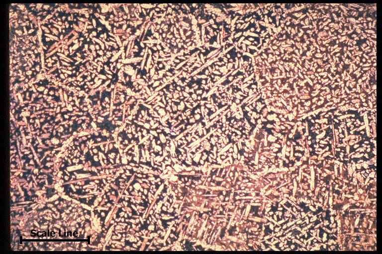
11 Microscopy Visible light: 0.4~0.7m Resolution limit ~ 0.5λ ~ 0.3µ Examined by the optical properties of the surface: need etching Depth of field is important: needs a flat surface (polishing) Up to 2000x Brass (annealing twins) FCC - Cu/Zn alloy Bronze (Cu/Sn alloy)
12
 2 = 6 grains/in 2 3.")
13 Grain Size ASTM (American Society for Testing And Materials) grain size number n With 100x N = 2 n 1 N = no. of grains/in 2 46 grains + 22 on circumference = /2 =57 grains N=57 / π (3.5/2) 2 = 6 grains/in =2 n-1, n=3.6 n N


14 Scanning Electron Microscope 2000x Condenser lens Electron gun High depth of field!!! Scan generator Scan coils Objective lens Specimen Detector Display & storage 10~50,000x Modes: Emissive, reflective, absorptive, X-ray, etc..
15
16

17 Transmission Electron Microscope - TEM In TEM, sample thickness < 1000A for electron transmission Electron gun Condenser lens Objective lens Specimen Up to 1,000,000x Magnifying lenses Camera Diffraction, Microscopy, Spectroscopy are all possible in the same column. Applications: determine dislocation, defects, micro-precipitates, etc..
18
Imperfections in atomic arrangements
 MME131: Lecture 9 Imperfections in atomic arrangements Part 2: 1D 3D Defects A. K. M. B. Rashid Professor, Department of MME BUET, Dhaka Today s Topics Classifications and characteristics of 1D 3D defects
Dept.of BME Materials Science Dr.Jenan S.Kashan 1st semester 2nd level. Imperfections in Solids
 Why are defects important? Imperfections in Solids Defects have a profound impact on the various properties of materials: Production of advanced semiconductor devices require not only a rather perfect
Introduction to Engineering Materials ENGR2000 Chapter 4: Imperfections in Solids. Dr. Coates
 Introduction to Engineering Materials ENGR000 Chapter 4: Imperfections in Solids Dr. Coates Learning Objectives 1. Describe both vacancy and self interstitial defects. Calculate the equilibrium number
IMPERFECTIONSFOR BENEFIT. Sub-topics. Point defects Linear defects dislocations Plastic deformation through dislocations motion Surface
 IMPERFECTIONSFOR BENEFIT Sub-topics 1 Point defects Linear defects dislocations Plastic deformation through dislocations motion Surface IDEAL STRENGTH Ideally, the strength of a material is the force necessary
12/10/09. Chapter 4: Imperfections in Solids. Imperfections in Solids. Polycrystalline Materials ISSUES TO ADDRESS...
 Chapter 4: ISSUES TO ADDRESS... What are the solidification mechanisms? What types of defects arise in solids? Can the number and type of defects be varied and controlled? How do defects affect material
Imperfections, Defects and Diffusion
 Imperfections, Defects and Diffusion Lattice Defects Week5 Material Sciences and Engineering MatE271 1 Goals for the Unit I. Recognize various imperfections in crystals (Chapter 4) - Point imperfections
Chapter 4: Imperfections (Defects) in Solids
 in Solids") Chapter 4: Imperfections (Defects) in Solids ISSUES TO ADDRESS... What types of defects exist in solids? How do defects affect material properties? Can the number and type of defects be varied and controlled?
Chapter 4: Imperfections (Defects) in Solids ISSUES TO ADDRESS... What types of defects exist in solids? How do defects affect material properties? Can the number and type of defects be varied and controlled?
Point Defects. Vacancies are the most important form. Vacancies Self-interstitials
 Grain Boundaries 1 Point Defects 2 Point Defects A Point Defect is a crystalline defect associated with one or, at most, several atomic sites. These are defects at a single atom position. Vacancies Self-interstitials
3. Solidification & Crystalline Imperfections
 3. Solidification & Crystalline Imperfections solidification (casting process) of metals divided into two steps (1) nucleation formation of stable nuclei in the melt (2) growth of nuclei into crystals
Microstructural Characterization of Materials
 Microstructural Characterization of Materials 2nd Edition DAVID BRANDON AND WAYNE D. KAPLAN Technion, Israel Institute of Technology, Israel John Wiley & Sons, Ltd Contents Preface to the Second Edition
Chapter Outline Dislocations and Strengthening Mechanisms. Introduction
 Chapter Outline Dislocations and Strengthening Mechanisms What is happening in material during plastic deformation? Dislocations and Plastic Deformation Motion of dislocations in response to stress Slip
Lecture # 11. Line defects (1D) / Dislocations
 / Dislocations") Lecture # 11 - Line defects (1-D) / Dislocations - Planer defects (2D) - Volume Defects - Burgers vector - Slip - Slip Systems in FCC crystals - Slip systems in HCP - Slip systems in BCC References: 1-
Lecture # 11 - Line defects (1-D) / Dislocations - Planer defects (2D) - Volume Defects - Burgers vector - Slip - Slip Systems in FCC crystals - Slip systems in HCP - Slip systems in BCC References: 1-
Lecture # 11 References:
 Lecture # 11 - Line defects (1-D) / Dislocations - Planer defects (2D) - Volume Defects - Burgers vector - Slip - Slip Systems in FCC crystals - Slip systems in HCP - Slip systems in BCC Dr.Haydar Al-Ethari
(a) Would you expect the element P to be a donor or an acceptor defect in Si?
 Would you expect the element P to be a donor or an acceptor defect in Si?") MSE 200A Survey of Materials Science Fall, 2008 Problem Set No. 2 Problem 1: At high temperature Fe has the fcc structure (called austenite or γ-iron). Would you expect to find C atoms in the octahedral
MSE 200A Survey of Materials Science Fall, 2008 Problem Set No. 2 Problem 1: At high temperature Fe has the fcc structure (called austenite or γ-iron). Would you expect to find C atoms in the octahedral
Kinematical theory of contrast
 Kinematical theory of contrast Image interpretation in the EM the known distribution of the direct and/or diffracted beam on the lower surface of the crystal The image on the screen of an EM = the enlarged
Solid. Imperfection in solids. Examples of Imperfections #2. Examples of Imperfections #1. Solid
 Solid Imperfection in solids By E-mail: Patama.V@chula.ac.th Solid State of materials Rigid Strong bonding ionic, van der aals, metal bonding normally has crystal structure Examples of Imperfections #
Introduction to Engineering Materials ENGR2000 Chapter 7: Dislocations and Strengthening Mechanisms. Dr. Coates
 Introduction to Engineering Materials ENGR2000 Chapter 7: Dislocations and Strengthening Mechanisms Dr. Coates An edge dislocation moves in response to an applied shear stress dislocation motion 7.1 Introduction
much research (in physics, chemistry, material science, etc.) have been done to understand the difference in materials properties.
 have been done to understand the difference in materials properties.") 1.1: Introduction Material science and engineering Classify common features of structure and properties of different materials in a well-known manner (chemical or biological): * bonding in solids are classified
1.1: Introduction Material science and engineering Classify common features of structure and properties of different materials in a well-known manner (chemical or biological): * bonding in solids are classified
Practical 2P8 Transmission Electron Microscopy
 Practical 2P8 Transmission Electron Microscopy Originators: Dr. N.P. Young and Prof. J. M. Titchmarsh What you should learn from this practical Science This practical ties-in with the lecture course on
Dislocations and Plastic Deformation
 Dislocations and Plastic Deformation Edge and screw are the two fundamental dislocation types. In an edge dislocation, localized lattice distortion exists along the end of an extra half-plane of atoms,
 Defects in solids http://www.bath.ac.uk/podcast/powerpoint/inaugural_lecture_250407.pdf http://www.materials.ac.uk/elearning/matter/crystallography/indexingdirectionsandplanes/indexing-of-hexagonal-systems.html
Material Science. Prof. Satish V. Kailas Associate Professor Dept. of Mechanical Engineering, Indian Institute of Science, Bangalore India
 Material Science Prof. Satish V. Kailas Associate Professor Dept. of Mechanical Engineering, Indian Institute of Science, Bangalore 560012 India Chapter 3. Imperfections in Solids Learning objectives:
TEM and Electron Diffraction Keith Leonard, PhD (1999) U. Cincinnati
 U. Cincinnati") TEM and Electron Diffraction Keith Leonard, PhD (1999) U. Cincinnati Electron Microscopes: Electron microscopes, such as the scanning electron microscope (SEM) and transmission electron microscope (TEM)
TEM and Electron Diffraction Keith Leonard, PhD (1999) U. Cincinnati Electron Microscopes: Electron microscopes, such as the scanning electron microscope (SEM) and transmission electron microscope (TEM)
Physics of Materials: Defects in Solids. Dr. Anurag Srivastava. Indian Institute of Information Technology and Manegement, Gwalior
 : Defects in Solids Dr. Anurag Srivastava Atal Bihari Vajpayee Indian Institute of Information Technology and Manegement, Gwalior What you have learnt so far? Properties of Materials affected by defects
Dislocations in Materials. Dislocations in Materials
 Pose the following case scenario: Consider a block of crystalline material on which forces are applied. Top Force (111) parallel with top surface Bottom Force Sum Sum of of the the applied forces give
Point coordinates. x z
 Point coordinates c z 111 a 000 b y x z 2c b y Point coordinates z y Algorithm 1. Vector repositioned (if necessary) to pass through origin. 2. Read off projections in terms of unit cell dimensions a,
EMSE Weak-Beam Dark-Field Technique
 Weak-Beam Dark-Field Technique 1 Weak-Beam Dark-Field Imaging Basic Idea recall bright-field contrast of dislocations: specimen close to Bragg condition, s î 0 near the dislocation core, some planes curved
ISSUES TO ADDRESS...
 Chapter 5: IMPERFECTIONS IN SOLIDS School of Mechanical Engineering Choi, Hae-Jin Materials Science - Prof. Choi, Hae-Jin Chapter 4-1 ISSUES TO ADDRESS... What are the solidification mechanisms? What types
Chapter 7 Dislocations and Strengthening Mechanisms. Dr. Feras Fraige
 Chapter 7 Dislocations and Strengthening Mechanisms Dr. Feras Fraige Chapter Outline Dislocations and Strengthening Mechanisms What is happening in material during plastic deformation? Dislocations and
STUDY & ANALYSIS OF ALUMINIUM FOIL AND ANATASE TITANIUM OXIDE (TiO2) USING TRANSMISSION ELECTRON MICROSCOPY
 USING TRANSMISSION ELECTRON MICROSCOPY") STUDY & ANALYSIS OF ALUMINIUM FOIL AND ANATASE TITANIUM OXIDE (TiO2) USING TRANSMISSION ELECTRON MICROSCOPY Ayush Garg Department of Chemical and Materials Engineering, University of Auckland, Auckland,
STUDY & ANALYSIS OF ALUMINIUM FOIL AND ANATASE TITANIUM OXIDE (TiO2) USING TRANSMISSION ELECTRON MICROSCOPY Ayush Garg Department of Chemical and Materials Engineering, University of Auckland, Auckland,
Twins & Dislocations in HCP Textbook & Paper Reviews. Cindy Smith
 Twins & Dislocations in HCP Textbook & Paper Reviews Cindy Smith Motivation Review: Outline Crystal lattices (fcc, bcc, hcp) Fcc vs. hcp stacking sequences Cubic {hkl} naming Hcp {hkil} naming Twinning
Strengthening Mechanisms
 ME 254: Materials Engineering Chapter 7: Dislocations and Strengthening Mechanisms 1 st Semester 1435-1436 (Fall 2014) Dr. Hamad F. Alharbi, harbihf@ksu.edu.sa November 18, 2014 Outline DISLOCATIONS AND
Imaging with Diffraction Contrast
 Imaging with Diffraction Contrast Duncan Alexander EPFL-CIME 1 Introduction When you study crystalline samples TEM image contrast is dominated by diffraction contrast. An objective aperture to select either
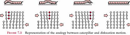
Movement of edge and screw dislocations
 Movement of edge and screw dislocations Formation of a step on the surface of a crystal by motion of (a) n edge dislocation: the dislocation line moves in the direction of the applied shear stress τ. (b)
Defect in crystals. Primer in Materials Science Spring
 Defect in crystals Primer in Materials Science Spring 2017 11.05.2017 1 Introduction The arrangement of the atoms in all materials contains imperfections which have profound effect on the behavior of the
TEM imaging and diffraction examples
 TEM imaging and diffraction examples Duncan Alexander EPFL-CIME 1 Diffraction examples Kikuchi diffraction Epitaxial relationships Polycrystalline samples Amorphous materials Contents Convergent beam electron
Point coordinates. Point coordinates for unit cell center are. Point coordinates for unit cell corner are 111
 Point coordinates c z 111 Point coordinates for unit cell center are a/2, b/2, c/2 ½ ½ ½ Point coordinates for unit cell corner are 111 x a z 000 b 2c y Translation: integer multiple of lattice constants
Materials Science. Imperfections in Solids CHAPTER 5: IMPERFECTIONS IN SOLIDS. Types of Imperfections
 In the Name of God Materials Science CHAPTER 5: IMPERFECTIONS IN SOLIDS ISSUES TO ADDRESS... What are the solidification mechanisms? What types of defects arise in solids? Can the number and type of defects
TOPIC 2. STRUCTURE OF MATERIALS III
 Universidad Carlos III de Madrid www.uc3m.es MATERIALS SCIENCE AND ENGINEERING TOPIC 2. STRUCTURE OF MATERIALS III Topic 2.3: Crystalline defects. Solid solutions. 1 PERFECT AND IMPERFECT CRYSTALS Perfect
CHEM-E5225 :Electron Microscopy Imaging II
 CHEM-E5225 :Electron Microscopy Imaging II D.B. Williams, C.B. Carter, Transmission Electron Microscopy: A Textbook for Materials Science, Springer Science & Business Media, 2009. Z. Luo, A Practical Guide
Transmission Electron Microscopy (TEM) Prof.Dr.Figen KAYA
 Prof.Dr.Figen KAYA") Transmission Electron Microscopy (TEM) Prof.Dr.Figen KAYA Transmission Electron Microscope A transmission electron microscope, similar to a transmission light microscope, has the following components along
Transmission Electron Microscopy (TEM) Prof.Dr.Figen KAYA Transmission Electron Microscope A transmission electron microscope, similar to a transmission light microscope, has the following components along
Silver Diffusion Bonding and Layer Transfer of Lithium Niobate to Silicon
 Chapter 5 Silver Diffusion Bonding and Layer Transfer of Lithium Niobate to Silicon 5.1 Introduction In this chapter, we discuss a method of metallic bonding between two deposited silver layers. A diffusion
Electron microscopy II
 Electron microscopy II Nanomaterials characterization I RNDr. Věra Vodičková, PhD. Interaction ction: electrons solid matter Signal types SE.secondary e - AE Auger s e - BSE back scattered e - X-ray photons,
Imperfections in the Atomic and Ionic Arrangements
 Objectives Introduce the three basic types of imperfections: point defects, line defects (or dislocations), and surface defects. Explore the nature and effects of different types of defects. Outline Point
Supplementary Material
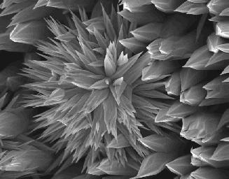
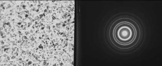
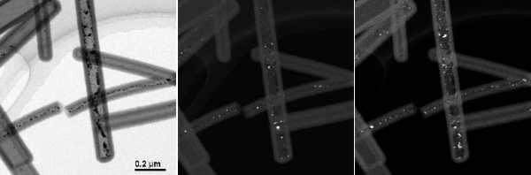
 Supplementary Material Self-patterning Gd nano-fibers in Mg-Gd alloys Yangxin Li 1,2, Jian Wang 3, Kaiguo Chen 4, Meiyue Shao 2, Yao Shen 1 *, Li Jin 2 *, Guozhen Zhu 1 * 1 State Key Laboratory of Metal
3. Anisotropic blurring by dislocations
 Dynamical Simulation of EBSD Patterns of Imperfect Crystals 1 G. Nolze 1, A. Winkelmann 2 1 Federal Institute for Materials Research and Testing (BAM), Berlin, Germany 2 Max-Planck- Institute of Microstructure
Solid State Device Fundamentals
 Solid State Device Fundamentals ENS 345 Lecture Course by Alexander M. Zaitsev alexander.zaitsev@csi.cuny.edu Tel: 718 982 2812 Office 4N101b 1 Solids Three types of solids classified according to atomic
Answer All Questions. All Questions Carry Equal Marks. Time: 20 Min. Marks: 10.
 Code No: 09A1BS02 Set No. 1 JAWAHARLAL NEHRU TECHNOLOGICAL UNIVERSITY HYDERABAD I B.Tech. I Mid Examinations, November 2009 ENGINEERING PHYSICS Objective Exam Name: Hall Ticket No. A Answer All Questions.
Chapter 4. Introduction to Dislocations
 Chapter 4 Introduction to Dislocations The discrepancy between the theoretical and observed yield stresses of crystals Dislocations The Burgers vector Vector notation for dislocations Dislocations in the
ECE236A Semiconductor Heterostructure Materials Defects in Semiconductor Crystals Lecture 6 Oct. 19, 2017
 ECE236A Semiconductor Heterostructure Materials Defects in Semiconductor Crystals Lecture 6 Oct. 19, 2017 Stacking sequence in simple crystals. Stacking faults (intrinsic, extrinsic) Twin boundaries Dislocations
Fundamentals of Plastic Deformation of Metals
 We have finished chapters 1 5 of Callister s book. Now we will discuss chapter 10 of Callister s book Fundamentals of Plastic Deformation of Metals Chapter 10 of Callister s book 1 Elastic Deformation
Planar Defects in Materials. Planar Defects in Materials
 Classification of Defects in Solids: Planar defects: Stacking faults o {311} defects in Si o Inversion domain boundaries o Antiphase boundaries (e.g., super dislocations): analogous to partials but in
Module-6. Dislocations and Strengthening Mechanisms
 Module-6 Dislocations and Strengthening Mechanisms Contents 1) Dislocations & Plastic deformation and Mechanisms of plastic deformation in metals 2) Strengthening mechanisms in metals 3) Recovery, Recrystallization
Chapter 5. Imperfections in Solids
 Chapter 5 Imperfections in Solids Chapter 5 2D Defects and Introduction to Diffusion Imperfections in Solids Issues to Address... What types of defects arise in solids? Can the number and type of defects
SECTION A. NATURAL SCIENCES TRIPOS Part IA. Friday 4 June to 4.30 MATERIALS AND MINERAL SCIENCES
 NATURAL SCIENCES TRIPOS Part IA Friday 4 June 1999 1.30 to 4.30 MATERIALS AND MINERAL SCIENCES Answer five questions; two from each of sections A and B and one from section C. Begin each answer at the
Effects of Metallographic Structures on the Properties of High-Performance Phosphor Bronze
 Effects of Metallographic Structures on the Properties of High-Performance Phosphor Bronze by Kuniteru Mihara *, Tatsuhiko Eguchi *, Takashi Yamamoto * and Akihiro Kanamori * As electronic equipment such
Defect and chemical analysis in the TEM
 THE UNIVERSITY Defect and chemical analysis in the TEM Defect and chemical analysis in the TEM I.P. Jones. Chemical analysis: EDX. Chemical analysis: PEELS Centre for Electron Microscopy OF BIRMINGHAM
Application of Scanning Electron Microscope to Dislocation Imaging in Steel
 Application of Scanning Electron Microscope to Dislocation Imaging in Steel Masaaki Sugiyama and Masateru Shibata Advanced Technology Research Laboratories, Nippon Steel Corporation SM Business Unit, JEOL
Student Name: ID Number:
 Student Name: ID Number: DEPARTMENT OF MECHANICAL ENGINEERING CONCORDIA UNIVERSITY MATERIALS SCIENCE - MECH 1/ - Sections T & X MIDTERM 003 Instructors: Dr. M.Pugh & Dr. M.Medraj Time Allowed: one (1)
Materials and their structures
 Materials and their structures 2.1 Introduction: The ability of materials to undergo forming by different techniques is dependent on their structure and properties. Behavior of materials depends on their
Thin Film Scattering: Epitaxial Layers
 Thin Film Scattering: Epitaxial Layers 6th Annual SSRL Workshop on Synchrotron X-ray Scattering Techniques in Materials and Environmental Sciences: Theory and Application May 29-31, 2012 Thin films. Epitaxial
Why does the growth rate slow down as a precipitate thickens during diffusion-controlled growth?
 Part II: Worked Examples H. K. D. H. Bhadeshia Question 14 Why does the growth rate slow down as a precipitate thickens during diffusion-controlled growth? The surface of a metal can be nitrided to form
SiC crystal growth from vapor
 SiC crystal growth from vapor Because SiC dissolves in Si and other metals can be grown from melt-solutions: Liquid phase epitaxy (LPE) Solubility of C in liquid Si is 0.029% at 1700oC high T process;
Practical 2P8 Transmission Electron Microscopy
 Practical 2P8 Transmission Electron Microscopy Originators: Dr. M. L. Jenkins and Prof. J. M. Titchmarsh What you should learn from this practical Science This practical ties-in with the lecture course
Chapter Outline How do atoms arrange themselves to form solids?
 Chapter Outline How do atoms arrange themselves to form solids? Fundamental concepts and language Unit cells Crystal structures Face-centered cubic Body-centered cubic Hexagonal close-packed Close packed
Experimental problem uniquely solved by TEM: Observation of dislocations and their dynamics. Milan Kornjaca, Physics 590B
 Experimental problem uniquely solved by TEM: Observation of dislocations and their dynamics Milan Kornjaca, Physics 590B 3000-year-old problem Why can metals be workhardened and annealed? Why is steel
Dr. Ali Abadi Chapter Three: Crystal Imperfection Materials Properties
 Dr. Ali Abadi Chapter Three: Crystal Imperfection Materials Properties A perfect crystal, with every atom of the same type in the correct position, does not exist. There always exist crystalline defects,
Deformation Criterion of Low Carbon Steel Subjected to High Speed Impacts
 Deformation Criterion of Low Carbon Steel Subjected to High Speed Impacts W. Visser, G. Plume, C-E. Rousseau, H. Ghonem 92 Upper College Road, Kingston, RI 02881 Department of Mechanical Engineering, University
How do you expect the packing factor to vary with coordination number?
 DATA SHEETS: Crystal Structures and Metallography Date: Lab Partners: Body Centered Cubic (BCC) Structure: CN: Atoms touch along: Number of atoms per unit cell: Determination of PF: Face Centered Cubic
Crystallographic Textures Measurement
 Crystallographic Textures Measurement D. V. Subramanya Sarma Department of Metallurgical and Materials Engineering Indian Institute of Technology Madras E-mail: vsarma@iitm.ac.in Macrotexture through pole
Defects and Diffusion
 Defects and Diffusion Goals for the Unit Recognize various imperfections in crystals Point imperfections Impurities Line, surface and bulk imperfections Define various diffusion mechanisms Identify factors
Materials Science and Engineering: An Introduction
 Materials Science and Engineering: An Introduction Callister, William D. ISBN-13: 9780470419977 Table of Contents List of Symbols. 1 Introduction. 1.1 Historical Perspective. 1.2 Materials Science and
Single vs Polycrystals
 WEEK FIVE This week, we will Learn theoretical strength of single crystals Learn metallic crystal structures Learn critical resolved shear stress Slip by dislocation movement Single vs Polycrystals Polycrystals
Chapter 8. Deformation and Strengthening Mechanisms
 Chapter 8 Deformation and Strengthening Mechanisms Chapter 8 Deformation Deformation and Strengthening Issues to Address... Why are dislocations observed primarily in metals and alloys? How are strength
Learning Objectives. Chapter Outline. Solidification of Metals. Solidification of Metals
 Learning Objectives Study the principles of solidification as they apply to pure metals. Examine the mechanisms by which solidification occurs. - Chapter Outline Importance of Solidification Nucleation
Chapter 7: Dislocations and strengthening mechanisms
 Chapter 7: Dislocations and strengthening mechanisms Introduction Basic concepts Characteristics of dislocations Slip systems Slip in single crystals Plastic deformation of polycrystalline materials Plastically
University of Pretoria Z Tang (2006) Chapter 8 Studies of acicular ferrite by thin foil TEM
 Chapter 8 Studies of acicular ferrite by thin foil TEM") 8.2 Two types of acicular ferrite 8.2.1 Structure with parallel laths There appeared to be two types of acicular ferrite laths that were observed in those alloys cooled with a rapid cooling rate of 47
8.2 Two types of acicular ferrite 8.2.1 Structure with parallel laths There appeared to be two types of acicular ferrite laths that were observed in those alloys cooled with a rapid cooling rate of 47
MACROSTRUCTURE, MICROSTRUCTURE AND MICROHARDNESS ANALYSIS
 109 Chapter 5 MACROSTRUCTURE, MICROSTRUCTURE AND MICROHARDNESS ANALYSIS 5.1 INTRODUCTION The microstructural studies of friction welding helps in understanding microstructural changes occurred during friction
Engineering materials
 1 Engineering materials Lecture 2 Imperfections and defects Response of materials to stress 2 Crystalline Imperfections (4.4) No crystal is perfect. Imperfections affect mechanical properties, chemical
TEM imaging and diffraction examples
 TEM imaging and diffraction examples Duncan Alexander EPFL-CIME 1 Diffraction examples Kikuchi diffraction Epitaxial relationships Polycrystalline samples Amorphous materials Contents Convergent beam electron
ISSUES TO ADDRESS... What types of defects arise in solids? Can the number and type of defects be varied and controlled?
 CHAPTER 4: IMPERFECTIONS IN SOLIDS ISSUES TO ADDRESS... What types of defects arise in solids? Can the number and type of defects be varied and controlled? How do defects affect material properties? Are
9.1 Refinement of dangling bond densities calculations
 I 9 9.1 Refinement of dangling bond densities calculations However, a situation when the combined case takes place may be also theoretically possible. For the instance, when condition of core at the 30
INTERPRETATION OF TRANSMISSION ELECTRON MICROGRAPHS
 3 INTERPRETATION OF TRANSMISSION ELECTRON MICROGRAPHS Already published in this series 1. The Operation and Calibration of the Electron Microscope 2. Electron Diffraction in the Electron Microscope In
STATE OF SOLIDIFICATION & CRYSTAL STRUCTURE
 STATE OF SOLIDIFICATION & CRYSTAL STRUCTURE Chapter Outline Determination of crystal properties or properties of crystalline materials. Crystal Geometry! Crystal Directions! Linear Density of atoms! Crystal
Chapter 3 Basic Crystallography and Electron Diffraction from Crystals. Lecture 9. Chapter 3 CHEM Fall, L. Ma
 Chapter 3 Basic Crystallography and Electron Diffraction from Crystals Lecture 9 Outline The geometry of electron diffraction Crystallography Kinetic Theory of Electron diffraction Diffraction from crystals
CME 300 Properties of Materials. ANSWERS Homework 2 September 28, 2011
 CME 300 Properties of Materials ANSWERS Homework 2 September 28, 2011 1) Explain why metals are ductile and ceramics are brittle. Why are FCC metals ductile, HCP metals brittle and BCC metals tough? Planes
Module #8. Defects in Crystalline Materials. READING LIST DIETER: Ch. 4, Pages
 HOMEWORK From Dieter 4-6 Module #8 Defects in Crystalline Materials READING LIST DIETER: Ch. 4, Pages 103-114 Ch. 4, Pages 103-117 in Meyers & Chawla, 1 st ed. Ch. 1, Pages 1-26 in Argon Property Structure,
Carnegie Mellon MRSEC
 Carnegie Mellon MRSEC Texture, Microstructure & Anisotropy, Fall 2009 A.D. Rollett, P. Kalu 1 ELECTRONS SEM-based TEM-based Koseel ECP EBSD SADP Kikuchi Different types of microtexture techniques for obtaining
CRYSTAL STRUCTURE, MECHANICAL BEHAVIOUR & FAILURE OF MATERIALS
 MODULE ONE CRYSTAL STRUCTURE, MECHANICAL BEHAVIOUR & FAILURE OF MATERIALS CRYSTAL STRUCTURE Metallic crystal structures; BCC, FCC and HCP Coordination number and Atomic Packing Factor (APF) Crystal imperfections:
Activation of deformation mechanism
 Activation of deformation mechanism The deformation mechanism activates when a critical amount of mechanical stress imposed to the crystal The dislocation glide through the slip systems when the required
1P1b: Introduction to Microscopy
 1P1b: Introduction to Microscopy Central to the study and characterisation of metals and many other materials is the microscope, ranging from the magnification of, say, 1 to 35 in a simple stereo binocular
CHAPTER 6 OUTLINE. DIFFUSION and IMPERFECTIONS IN SOLIDS
 CHAPTER 6 DIFFUSION and IMPERFECTIONS IN SOLIDS OUTLINE 1. TYPES OF DIFFUSIONS 1.1. Interdiffusion 1.2. Selfdiffusion 1.3.Diffusion mechanisms 1.4.Examples 2. TYPES OF IMPERFECTIONS 2.1.Point Defects 2.2.Line
Chapter Outline. How do atoms arrange themselves to form solids?
 Chapter Outline How do atoms arrange themselves to form solids? Fundamental concepts and language Unit cells Crystal structures! Face-centered cubic! Body-centered cubic! Hexagonal close-packed Close packed
Imperfections: Good or Bad? Structural imperfections (defects) Compositional imperfections (impurities)
 Compositional imperfections (impurities)") Imperfections: Good or Bad? Structural imperfections (defects) Compositional imperfections (impurities) 1 Structural Imperfections A perfect crystal has the lowest internal energy E Above absolute zero
Imperfections: Good or Bad? Structural imperfections (defects) Compositional imperfections (impurities) 1 Structural Imperfections A perfect crystal has the lowest internal energy E Above absolute zero
Observation in the GB (Gentle Beam) Capabilities
 Capabilities") A field-emission cathode in the electron gun of a scanning electron microscope provides narrower probing beams at low as well as high electron energy, resulting in both improved spatial resolution and
A field-emission cathode in the electron gun of a scanning electron microscope provides narrower probing beams at low as well as high electron energy, resulting in both improved spatial resolution and
Crystal Defects. Perfect crystal - every atom of the same type in the correct equilibrium position (does not exist at T > 0 K)
") Crystal Defects Perfect crystal - every atom of the same type in the correct equilibrium position (does not exist at T > 0 K) Real crystal - all crystals have some imperfections - defects, most atoms are
Crystal Defects Perfect crystal - every atom of the same type in the correct equilibrium position (does not exist at T > 0 K) Real crystal - all crystals have some imperfections - defects, most atoms are
Dislocations & Materials Classes. Dislocation Motion. Dislocation Motion. Lectures 9 and 10
 Lectures 9 and 10 Chapter 7: Dislocations & Strengthening Mechanisms Dislocations & Materials Classes Metals: Disl. motion easier. -non-directional bonding -close-packed directions for slip. electron cloud
9/28/2013 9:26 PM. Chapter 3. The structure of crystalline solids. Dr. Mohammad Abuhaiba, PE
 Chapter 3 The structure of crystalline solids 1 2 Why study the structure of crystalline solids? Properties of some materials are directly related to their crystal structure. Significant property differences
Observation of Al-lines in LSI devices by ultra-high voltage electron microscope
 Microsc. Microanal. Microstruct. 4 (1993) 239 APRIUJUNE 1993, PAGE 239 Classification Physics Abstracts 07.80-73.90 Observation of Al-lines in LSI devices by ultra-high voltage electron microscope Akio
Thin Film Scattering: Epitaxial Layers
 Thin Film Scattering: Epitaxial Layers Arturas Vailionis First Annual SSRL Workshop on Synchrotron X-ray Scattering Techniques in Materials and Environmental Sciences: Theory and Application Tuesday, May