Carbon Nanotube Templated- Microfabricated Thin Layer Chromatography Plates
|
|
|
- Rolf Barber
- 5 years ago
- Views:
Transcription

1 Carbon Nanotube Templated- Microfabricated Thin Layer Chromatography Plates David S. Jensen, 1 Supriya Kenyal, 1 Ricky Wyman, 1 Robert Davis, 1 Richard Vanfleet, 1 Andrew Dadson, 2 Michael Vail, 2 Matthew R. Linford 1* 1 Brigham Young University, Provo, UT, USA 2 US Synthetic Corporation, Orem, UT, USA
2 Presentation Outline Current TLC technology Why produce a microfabricated TLC plate How the TLC plates are fabricated Studies using a diamond geometry patterned surface Studies using a zigzag patterned surface Comparison with current HPTLC and UTLC plates Further work

3 Properties of Si 60 TLC and HPTLC plates
4 Why microfabricate a TLC plate TLC and HPTLC plates are produced by creating a slurry of adsorbent and then smearing the slurry across the backing. This produces a random bed of adsorbent The SiO 2 adsorbent is bound together by a low concentration of low molecular weight polymer or calcium sulfate (gypsum) Why microfabrication? Goal: create a separation medium that will significantly reduce analyst time and improve chromatographic characteristics. Theoretical studies show that an increase in the homogeneity of the adsorbent bed improves the chromatographic efficiency for pressure driven systems. 1,2 Microfabrication allows for precise placement of the chromatographic adsorbent. 1. De Smet, J. et al. Anal. Chem. 2004, 76, Billen, J. et al. J. Chromatogr. A 2007, 1168, 73-99

 are grown with C 2 H 4, H 2, and Ar as the processing gases. Heights can range from 10 µm to 2 mm.")
5 Fabrication Scheme After Reduce reducing the patterned the iron iron catalyst with and H 2 forming argon while the temperature is nanoparticles ramped up to the 750 C. This process carbon forms nanotubes iron nanoparticles. (CNTs) are grown with C 2 H 4, H 2, and Ar as the processing gases. Heights can range from 10 µm to 2 mm. Iron catalyst Al 2 O 3 (Diffusion barrier, limits the formation of iron silicide) Backing Material (Silicon wafer)


6 Coating the CNTs with silicon SiH4(g) Si(g) + 2H2(g) TEM image showing the silicon used encapsulated as the CNTS SiH4 is processing reagent to coat CNT the CNTs with amorphous silicon. This is a low Si coating pressure chemical deposition process at a temperature of 530 CSEM micrograph of silicon coated CNTs. This process produces a mechanically stable material. However, the material at this point is dark and is difficult to see separated analytes Al2O3 (Diffusion barrier, limits the formation of iron silicide) Backing Material (Silicon wafer)

7 Converting the Silicon to Silica Oxidation of the of material the material in in atmosphere 1000 C removes at 1000 C removes the CNTs and converts the silicon to the silica. CNTs After and which converts the material the silicon is to hydrated silica. with After an which acidic solution the material (1:1 is hydrated 0.1 M HCl:MeOH) with an prior acidic to solution chromatography (1:1 0.1 M HCl:MeOH) to increase the silanol content prior to chromatography
8 Microfabrication Process Scheme at a Glance Backing Material Photolithography Barrier Layer Al 2 O 3 (30 nm) Catalytic Material Iron (6 nm) Remove Photo Resist CNT Growth CVD Process LPCVD Process Infiltrate with Silicon Oxidize CNTs out Oxidize Si to SiO 2 After the fabrication process the silanol content of the adsorbent needs to be increased. The TLC plate is placed into a bath of 1:1 HCl(0.1 M):Methanol at reflux temperatures for overnight. After the rehydration process the TLC plate is rinsed thoroughly with water to remove any residual acid. Then the plate is dried at 110 C and is now ready for chromatography.


9 SEM micrographs of the final product Side image Top View
10 Microfabrication process: Placement of the Iron catalyst Photolithography was used to place the iron catalyst 10 x 5 µm diamond geometry Sight the paper that speaks about the theoretical use of the diamond geometry and the other microfluidic devices that have used this type of design
11 2:1 Aspect Ratio Diamond Geometry Bird s eye view of the TLC plate Different channel widths create different flow velocities and distorts the chromatography Dimensions: 10 x 5 µm pillar 4 µm bed spacing 100 µm tall When the CNT features were grown tall they tend to lean This creates inhomogenaties for solvent flow


12 Chromatography A test dye mixture from CAMAG (Muttenz, Switzerland) was used for chromatographic evaluation Mobile phase was toluene The plate has chromatographic abilities! The analytes wander during the separation process The chromatography does suffer from this random adsorbent bed created from the mechanical instability of the CNTs
13 What needs to be fixed? The mechanical strength of the CNT framework needs to be increased. This has been done by the use of a zigzag pattern. The zigzag pattern approximates a parallel plate geometry which has shown to give the best theoretical plate height in chromatography. 1,2 1. De Smet, J. et al. Anal. Chem. 2004, 76, Billen, J. et al. J. Chromatogr. A 2007, 1168, 73-99


14 Run Time 12 mins 37 sec Mobile Phase: Toluene (3mL) Migration distance: 45 mm Relative Humidity: 42% CAMAG Test Dye Mixture III Dispersed in Hexanes 3%v/v and 10% v/v Finish Plate I Prior Oxidation Dimensions Adsorbent layer thickness: 50 µm Nominal Hedge Thickness: 5 µm Nominal Channel Width: 9 µm After oxidation Hedge With: 8.3 ± 0.4 µm: Channel Width: Closed off These plate number are comparable to HPTLC plates Channels are closed off Start 3% 3% 10% 10% and 3% are v/v of CAMAG test dye into hexanes Features are closed off, this leads to a slow development time of ca. 12 minutes


15 Run Time 2 mins 59 sec Mobile Phase: Toluene (3mL) Migration distance: 45 mm Relative Humidity: 41% CAMAG Test Dye Mixture III Dispersed in Hexanes 3%v/v and 10% v/v Plate II Prior Oxidation Dimensions Adsorbent layer thickness: 50 µm Nominal Hedge Thickness: 5 µm Nominal Channel Width: 11 µm After oxidation Hedge With: 7.2± 0.3 µm: Channel Width: 4.8 ± 2.0 µm Finish Start The features are now opened introducing faster capillary flow giving a development time of 3 minutes 3% 3% 10%


16 Run Time 2 mins 20 sec Mobile Phase: Toluene (3mL) Migration distance: 45 mm Relative Humidity: 42% CAMAG Test Dye Mixture III Dispersed in Hexanes 3%v/v and 10% v/v Plate III Finish Start 3% 3% 10% Prior Oxidation Dimensions Adsorbent layer thickness: 50 µm Nominal Hedge Thickness: 5 µm Nominal Channel Width: 13 µm After oxidation Hedge With: 7.4.± 0.2 µm: Channel Width: 6.7 ± 1.9 µm Development time: 2 minutes and 20 seconds


17 Run Time 2 mins 4 secs Mobile Phase: Toluene (3mL) Migration distance: 45 mm Relative Humidity: 42% CAMAG Test Dye Mixture III Dispersed in Hexanes 3%v/v and 10% v/v Plate IV Finish Prior Oxidation Dimensions Adsorbent layer thickness: 50 µm Nominal Hedge Thickness: 5 µm Nominal Channel Width: 15 µm After oxidation Hedge With: 7.4 ± 0.2 µm: Channel Width: 7.0 ± 2.7 µm Start Development time: 2 minutes and 4 seconds 3% 3% 10%
18 van Deemter like plots

19 UTLC by Merck Chromatography was preformed under the same conditions that were used for the microfabricated TLC plates. Development time: 22 min 10 sec SiO 2 -layer of 10 µm has mesopores of 3-4 nm and macropores of 1-2µm

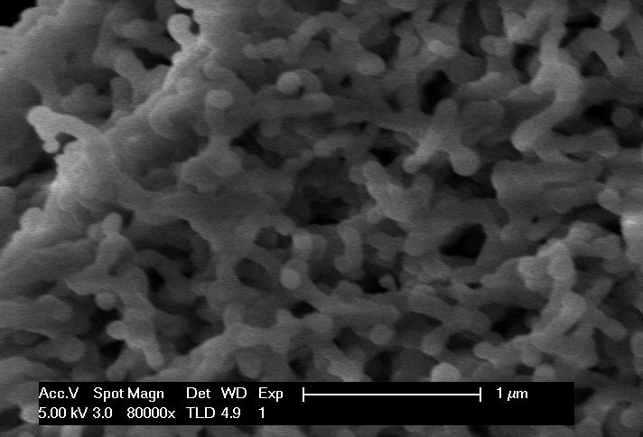
20 HPTLC LiChrospher from Merck Chromatography was preformed under the same conditions that were used for the microfabricated TLC plates. Layer thickness: 200 µm Particles: Spherical with a mean PSD of 7 µm The chromatography doesn t have baseline separation. There is also binder that is included as seen in this SEM micrograph
 (baseline separation but long development time) LiChrospher HPTLC (no baseline separation) Merck TLC (no baseline")
21 Run Times: 2 min 20 sec Comparison of R f and development times 22 min 10 sec 4 min 28 sec 4 min 30 sec Plate III CNT-M TLC Merck UTLC (baseline separation) (baseline separation but long development time) LiChrospher HPTLC (no baseline separation) Merck TLC (no baseline separation)
22 Areas of Improvement A reduction in the width of the adsorbent is effectively decreasing the particle size. There are significant improvements that can still be made. H = A + B/u + Cu Understanding how a change in the channel width effects the flow velocity and chromatographic abilities. Surface silanization will be possible to produce different phases C 18, -C 8, -C 4, -NH 2, -diol, etc.
23 Acknowledgements Brigham Young University Department of Chemistry and Biochemistry The Linford group US Synthetic Corporation For Financial Support
24 Questions?
25
The effects of Fe/Al 2 O 3 preparation technique as a catalyst on synthesized CNTs in CVD method.
 Science Journal of Physics Science Journal Publication Science Journal of Physics Web: http://www.sjpublication.com/sjp.html The effects of Fe/Al 2 O 3 preparation technique as a catalyst on synthesized
S. W. Husain 1, V. Kiarostami 1, M. Morrovati 2, and M. R. Tagebakhsh 2
 ACTA CHROMATOGRAPHICA, NO. 13, 2003 MULTIRESIDUE DETERMINATION OF DIAZINON AND ETHION IN PISTACHIO NUTS BY USE OF MATRIX SOLID PHASE DISPERSION WITH A LANTHANUM SILICATE CO-COLUMN AND GAS CHROMATOGRAPHY
Ultrathin layer chromatography using
 Ultrathin layer chromatography using electrospun nanofibers SusanV. Olesik Department of Chemistry Ohio State University International Symposium for High-Performance Thin-Layer Chromatography Basel July
Plateau-Rayleigh crystal growth of nanowire. heterostructures: Strain-modified surface chemistry
 Supporting Information for: Plateau-Rayleigh crystal growth of nanowire heterostructures: Strain-modified surface chemistry and morphological control in 1, 2 and 3 dimensions Robert W. Day, Max N. Mankin,
Czochralski Crystal Growth
 Czochralski Crystal Growth Crystal Pulling Crystal Ingots Shaping and Polishing 300 mm wafer 1 2 Advantage of larger diameter wafers Wafer area larger Chip area larger 3 4 Large-Diameter Wafer Handling
Scott Black. Maximizing Carbon Nanotube Forest Growth with 99.5% Pure Ethylene. Applied Physics Capstone Project Report. Physics 492R.
 Scott Black Maximizing Carbon Nanotube Forest Growth with 99.5% Pure Ethylene Applied Physics Capstone Project Report Physics 492R 31 July 2009 Advisors: Dr. Robert Davis and Dr. Richard Vanfleet Copyright
Complexity of IC Metallization. Early 21 st Century IC Technology
 EECS 42 Introduction to Digital Electronics Lecture # 25 Microfabrication Handout of This Lecture. Today: how are Integrated Circuits made? Silicon wafers Oxide formation by growth or deposition Other
Lecture 19 Microfabrication 4/1/03 Prof. Andy Neureuther
 EECS 40 Spring 2003 Lecture 19 Microfabrication 4/1/03 Prof. ndy Neureuther How are Integrated Circuits made? Silicon wafers Oxide formation by growth or deposition Other films Pattern transfer by lithography
Microfabrication of Integrated Circuits
 Microfabrication of Integrated Circuits OUTLINE History Basic Processes Implant; Oxidation; Photolithography; Masks Layout and Process Flow Device Cross Section Evolution Lecture 38, 12/05/05 Reading This
Process steps for Field Emitter devices built on Silicon wafers And 3D Photovoltaics on Silicon wafers
 Process steps for Field Emitter devices built on Silicon wafers And 3D Photovoltaics on Silicon wafers David W. Stollberg, Ph.D., P.E. Research Engineer and Adjunct Faculty GTRI_B-1 Field Emitters GTRI_B-2
HOMEWORK 4 and 5. March 15, Homework is due on Monday March 30, 2009 in Class. Answer the following questions from the Course Textbook:
 HOMEWORK 4 and 5 March 15, 2009 Homework is due on Monday March 30, 2009 in Class. Chapter 7 Answer the following questions from the Course Textbook: 7.2, 7.3, 7.4, 7.5, 7.6*, 7.7, 7.9*, 7.10*, 7.16, 7.17*,
Metal-Organic Frameworks for Thin-Layer Chromatographic Applications
 Supporting Information for: Metal-Organic Frameworks for Thin-Layer Chromatographic Applications Claudia Schenk, Christel Kutzscher, Franziska Drache, Stella Helten, Irena Senkovska and Stefan Kaskel*
Nonplanar Metallization. Planar Metallization. Professor N Cheung, U.C. Berkeley
 Nonplanar Metallization Planar Metallization Passivation Metal 5 (copper) Metal 3 (copper) Interlevel dielectric (ILD) Via (tungsten) Metal 1 (copper) Tungsten Plug to Si Silicon Caps and Plugs oxide oxide
Solutions Flash Automotive applications benefit from cost-effective, high chromium Amdry Braze Alloys. SF October 2014
 Solutions Flash Automotive applications benefit from cost-effective, high chromium Amdry Braze Alloys SF-0007.4 October 2014 Today s situation In the past two decades, many automotive components previously
CHAPTER 4 SYNTHESIS, CHARACTERIZATION AND MICROENCAPSULATION PROCESS OF THE NANO SILICA
 70 CHAPTER 4 SYNTHESIS, CHARACTERIZATION AND MICROENCAPSULATION PROCESS OF THE NANO SILICA 4.1 INTRODUCTION This chapter is concerned with the synthesis of nano silica particles from the natural resources
Supplementary Information
 Supplementary Information Atmospheric microplasma-functionalized 3D microfluidic strips within dense carbon nanotube arrays confine Au nanodots for SERS sensing Samuel Yick, Zhao Jun Han and Kostya (Ken)
Growth of monocrystalline In 2 O 3 nanowires by seed orientation dependent vapour-solid-solid mechanism
 Electronic Supplementary Material (ESI) for Journal of Materials Chemistry C. This journal is The Royal Society of Chemistry 2014 Electronic Supplementary Information (ESI) Growth of monocrystalline In
Metallization deposition and etching. Material mainly taken from Campbell, UCCS
 Metallization deposition and etching Material mainly taken from Campbell, UCCS Application Metallization is back-end processing Metals used are aluminum and copper Mainly involves deposition and etching,
Laser-derived One-Pot Synthesis of Silicon Nanocrystals Terminated with Organic Monolayers
 Electronic Supplementary Information for: Laser-derived One-Pot Synthesis of Silicon Nanocrystals Terminated with Organic Monolayers N. Shirahata,*,a M. R. Linford, b S. Furumi, a L. Pei, b Y. Sakka, a
Lecture Day 2 Deposition
 Deposition Lecture Day 2 Deposition PVD - Physical Vapor Deposition E-beam Evaporation Thermal Evaporation (wire feed vs boat) Sputtering CVD - Chemical Vapor Deposition PECVD LPCVD MVD ALD MBE Plating
Workshop on Nanoscience and Catalysts March 2008, QAU, Islamabad Nanocomposites for Thermal management Applications
 Fazal Ahmad Khalid Pro-Rector GIK Institute of Engineering Sciences and Technology Topi, NWFP, Pakistan (Khalid@giki.edu.pk) Workshop on Nanoscience and Catalysts 24-25 March 2008, QAU, Islamabad Nanocomposites
Dispersion of multi-walled carbon nanotubes in an aqueous medium by water dispersible- conjugated polymer nanoparticles
 Supplementary Material (ESI) for Chemical Communications This journal is (c) The Royal Society of Chemistry 2010 Supporting information Dispersion of multi-walled carbon nanotubes in an aqueous medium
Rapid Prototyping of Purification Platforms
 Rapid Prototyping of Purification Platforms Tom Huang, Nathan Mosier, Michael Ladisch Department of Agricultural and Biological Engineering Weldon School of Biomedical Engineering Laboratory of Renewable
Nanodiamond-Polymer Composite Fibers and Coatings
 Nanodiamond-Polymer Composite Fibers and Coatings Yury Gogotsi et al. A.J. Drexel Nanotechnology Institute and Department of Materials Science and Engineering Drexel University, Philadelphia, Pennsylvania
CHAPTER 4: The wetting behaviour and reaction of the diamond-si system
 CHAPTER 4: The wetting behaviour and reaction of the diamond-si system In this chapter, the wetting behaviour of diamond by silicon will be presented, followed by the study of the interaction between diamond
Improvement of gas barrier properties by combination of polymer film and gas barrier layer
 Improvement of gas barrier properties by combination of polymer film and gas barrier Y. Tsumagari, H. Murakami, K. Iseki and S. Yokoyama Toyobo Co., LTD. RESEARCH CENTER, - Katata 2-chome, Otsu, Shiga,
Structure and Chemical Analysis of Carbon Nanotubes Grown on Diamond Substrate Using Three Different Techniques MRS: November 30, 2010
 Structure and Chemical Analysis of Carbon Nanotubes Grown on Diamond Substrate Using Three Different Techniques MRS: November 30, 2010 Betty T. Quinton Wright State University, PhD. Student Material Science
Fabrication and Application of Vertically Aligned Carbon Nanotube Templated Silicon Nanomaterials
 Brigham Young University BYU ScholarsArchive All Theses and Dissertations 2011-10-26 Fabrication and Application of Vertically Aligned Carbon Nanotube Templated Silicon Nanomaterials Jun Song Brigham Young
EECS130 Integrated Circuit Devices
 EECS130 Integrated Circuit Devices Professor Ali Javey 9/13/2007 Fabrication Technology Lecture 1 Silicon Device Fabrication Technology Over 10 15 transistors (or 100,000 for every person in the world)
Fabrication Techniques for Thin-Film Silicon Layer Transfer
 Fabrication Techniques for Thin-Film Silicon Layer Transfer S. L. Holl a, C. A. Colinge b, S. Song b, R. Varasala b, K. Hobart c, F. Kub c a Department of Mechanical Engineering, b Department of Electrical
Ultra High Barrier Coatings by PECVD
 Society of Vacuum Coaters 2014 Technical Conference Presentation Ultra High Barrier Coatings by PECVD John Madocks & Phong Ngo, General Plasma Inc., 546 E. 25 th Street, Tucson, Arizona, USA Abstract Silicon
Synthesis of Multi Wall Carbon Nanotube (WCNT) over thin films of SiO 2 -Fe 2 O 3 deposited by Combustion Chemical Vapor Deposition
 over thin films of SiO 2 -Fe 2 O 3 deposited by Combustion Chemical Vapor Deposition") Synthesis of Multi Wall Carbon Nanotube (WCNT) over thin films of SiO 2 -Fe 2 O 3 deposited by Combustion Chemical Vapor Deposition M. D. Lima*, S. S. Stein, R. Bonadiman, M. J. de Andrade, C. P. Bergmann
Synthesis of Multi Wall Carbon Nanotube (WCNT) over thin films of SiO 2 -Fe 2 O 3 deposited by Combustion Chemical Vapor Deposition M. D. Lima*, S. S. Stein, R. Bonadiman, M. J. de Andrade, C. P. Bergmann
Ceramic and glass technology
 1 Row materials preperation Plastic Raw materials preperation Solid raw materials preperation Aging wet milling mastication Mixing seving Grain size reduction Milling Crushing Very fine milling Fine milling
Guowu Zhan and Hua Chun Zeng*
 Guowu Zhan and Hua Chun Zeng* NUS Graduate School for Integrative Sciences and Engineering, and Department of Chemical and Biomolecular Engineering, Faculty of Engineering, National University of Singapore,
Mater. Res. Soc. Symp. Proc. Vol Materials Research Society
 Mater. Res. Soc. Symp. Proc. Vol. 940 2006 Materials Research Society 0940-P13-12 A Novel Fabrication Technique for Developing Metal Nanodroplet Arrays Christopher Edgar, Chad Johns, and M. Saif Islam
Fabrication Process. Crystal Growth Doping Deposition Patterning Lithography Oxidation Ion Implementation CONCORDIA VLSI DESIGN LAB
 Fabrication Process Crystal Growth Doping Deposition Patterning Lithography Oxidation Ion Implementation 1 Fabrication- CMOS Process Starting Material Preparation 1. Produce Metallurgical Grade Silicon
Electron Microscopy Investigation at the Initial Growth Stage of Carbon Nanotubes
 Journal of the Korean Physical Society, Vol. 42, February 2003, pp. S727 S731 Electron Microscopy Investigation at the Initial Growth Stage of Carbon Nanotubes Sung-Jin Eum, Hee-Kwang Kang, Cheol-Woong
Chemical Vapor Deposition
 Chemical Vapor Deposition ESS4810 Lecture Fall 2010 Introduction Chemical vapor deposition (CVD) forms thin films on the surface of a substrate by thermal decomposition and/or reaction of gas compounds
TED PELLA, INC. Microscopy Products for Science and Industry
 PELCO SILICON NITRIDE, SILICON DIOXIDE, BLANK SILICON SUBSTRATES & APERTURES FOR TEM Clean, Debris-free with Exact 3mm TEM Frame and EasyGrip Edges PELCO Silicon Nitride Support Films for TEM Hydrophilic
Surface Micromachining
 Surface Micromachining Micro Actuators, Sensors, Systems Group University of Illinois at Urbana-Champaign Outline Definition of surface micromachining Most common surface micromachining materials - polysilicon
IC/MEMS Fabrication - Outline. Fabrication
 IC/MEMS Fabrication - Outline Fabrication overview Materials Wafer fabrication The Cycle: Deposition Lithography Etching Fabrication IC Fabrication Deposition Spin Casting PVD physical vapor deposition
ECSE-6300 IC Fabrication Laboratory Lecture 4: Dielectrics and Poly-Si Deposition. Lecture Outline
 ECSE-6300 IC Fabrication Laboratory Lecture 4: Dielectrics and Poly-Si Deposition Prof. Rensselaer Polytechnic Institute Troy, NY 12180 Office: CII-6229 Tel.: (518) 276-2909 e-mails: luj@rpi.edu http://www.ecse.rpi.edu/courses/s18/ecse
In situ generation of Li 2 FeSiO 4 coating on MWNT as a high rate cathode material for lithium ion batteries
 Supporting Information: In situ generation of Li 2 FeSiO 4 coating on MWNT as a high rate cathode material for lithium ion batteries Yi Zhao, Jiaxin Li, Ning Wang, Chuxin Wu, Yunhai Ding, Lunhui Guan*
Microelettronica. Planar Technology for Silicon Integrated Circuits Fabrication. 26/02/2017 A. Neviani - Microelettronica
 Microelettronica Planar Technology for Silicon Integrated Circuits Fabrication 26/02/2017 A. Neviani - Microelettronica Introduction Simplified crosssection of an nmosfet and a pmosfet Simplified crosssection
GROWTH MECHANISM OF NANODIMENSIONAL VANADIUM DIOXIDE ON SILICON SURFACE OBTAINED BY ML-ALD METHOD
 184 Rev. Adv. Mater. Sci. 27 (2011) 184-188 O.M. Osmolowskaya and V.M. Smirnov GROWTH MECHANISM OF NANODIMENSIONAL VANADIUM DIOXIDE ON SILICON SURFACE OBTAINED BY ML-ALD METHOD Saint-Petersburg State University,
Metallization. Typical current density ~10 5 A/cm 2 Wires introduce parasitic resistance and capacitance
 Metallization Interconnects Typical current density ~10 5 A/cm 2 Wires introduce parasitic resistance and capacitance RC time delay Inter-Metal Dielectric -Prefer low dielectric constant to reduce capacitance
Supporting Information. Low temperature synthesis of silicon carbide nanomaterials using
 Supporting Information Low temperature synthesis of silicon carbide nanomaterials using solid-state method Mita Dasog, Larissa F. Smith, Tapas K. Purkait and Jonathan G. C. Veinot * Department of Chemistry,
Introduction to Nanotechnology: Looking At Nanoparticles
 Introduction to Nanotechnology Nanotechnology is defined as the study and use of structures between 1 nanometer and 100 nanometers in size. To give you an idea of how small that is, it would take eight
Lab #2 Wafer Cleaning (RCA cleaning)
") Lab #2 Wafer Cleaning (RCA cleaning) RCA Cleaning System Used: Wet Bench 1, Bay1, Nanofabrication Center Chemicals Used: H 2 O : NH 4 OH : H 2 O 2 (5 : 1 : 1) H 2 O : HF (10 : 1) H 2 O : HCl : H 2 O 2
Lab #2 Wafer Cleaning (RCA cleaning) RCA Cleaning System Used: Wet Bench 1, Bay1, Nanofabrication Center Chemicals Used: H 2 O : NH 4 OH : H 2 O 2 (5 : 1 : 1) H 2 O : HF (10 : 1) H 2 O : HCl : H 2 O 2
EE 527 MICROFABRICATION. Lecture 15 Tai-Chang Chen University of Washington EE-527 M4 MASK SET: NPN BJT. C (sub) A E = 40 µm x 40 µm
 A E = 40 µm x 40 µm") EE 527 MICROFABRICATION Lecture 15 Tai-Chang Chen University of Washington EE-527 M4 MASK SET: NPN BJT C (sub) E B A E = 40 µm x 40 µm 1 EE-527 M4 MASK SET: MOS C-V TEST CAPACITORS W = 10 µm L = 10 µm
EE 527 MICROFABRICATION Lecture 15 Tai-Chang Chen University of Washington EE-527 M4 MASK SET: NPN BJT C (sub) E B A E = 40 µm x 40 µm 1 EE-527 M4 MASK SET: MOS C-V TEST CAPACITORS W = 10 µm L = 10 µm
Lecture 22: Integrated circuit fabrication
 Lecture 22: Integrated circuit fabrication Contents 1 Introduction 1 2 Layering 4 3 Patterning 7 4 Doping 8 4.1 Thermal diffusion......................... 10 4.2 Ion implantation.........................
Spray Drying Method for Large-Scale and High. Performance Silicon Negative Electrodes in Li-ion. Batteries
 SUPPORTING INFORMATION Spray Drying Method for Large-Scale and High Performance Silicon Negative Electrodes in Li-ion Batteries Dae Soo Jung, Tae Hoon Hwang, Seung Bin Park, and Jang Wook Choi,,* Graduate
Growth and Doping of SiC-Thin Films on Low-Stress, Amorphous Si 3 N 4 /Si Substrates for Robust Microelectromechanical Systems Applications
 Journal of ELECTRONIC MATERIALS, Vol. 31, No. 5, 2002 Special Issue Paper Growth and Doping of SiC-Thin Films on Low-Stress, Amorphous Si 3 N 4 /Si Substrates for Robust Microelectromechanical Systems
Temperature Scales. Questions. Temperature Conversions 7/21/2010. EE580 Solar Cells Todd J. Kaiser. Thermally Activated Processes
 7/1/010 EE80 Solar Cells Todd J. Kaiser Flow of Wafer in Fabrication Lecture 0 Microfabrication A combination of Applied Chemistry, Physics and ptics Thermal Processes Diffusion & xidation Photolithograpy
Copper Interconnect Technology
 Tapan Gupta Copper Interconnect Technology i Springer Contents 1 Introduction 1 1.1 Trends and Challenges 2 1.2 Physical Limits and Search for New Materials 5 1.3 Challenges 6 1.4 Choice of Materials 7
Rice husks as a sustainable source of nanostructured silicon for high performance Li-ion battery anodes
 Supplementary Information Rice husks as a sustainable source of nanostructured silicon for high performance Li-ion battery anodes Nian Liu 1, Kaifu Huo 2,3, Matthew T. McDowell 2, Jie Zhao 2 & Yi Cui 2,4
Supplementary Figure S1 Photograph of MoS 2 and WS 2 flakes exfoliated by different metal naphthalenide (metal = Na, K, Li), and dispersed in water.
, and dispersed in water.") Supplementary Figure S1 Photograph of MoS 2 and WS 2 flakes exfoliated by different metal naphthalenide (metal = Na, K, Li), and dispersed in water. Supplementary Figure S2 AFM measurement of typical LTMDs
Supplementary Figure S1 Photograph of MoS 2 and WS 2 flakes exfoliated by different metal naphthalenide (metal = Na, K, Li), and dispersed in water. Supplementary Figure S2 AFM measurement of typical LTMDs
Microstructured Optical Fibers as New Nanotemplates for High Pressure CVD
 Mater. Res. Soc. Symp. Proc. Vol. 988 2007 Materials Research Society 0988-QQ04-02 Microstructured Optical Fibers as New Nanotemplates for High Pressure CVD Neil Baril 1, John Badding 1, Pier Savio 2,
Supporting Information. Methanol Microreformer
 Supporting Information O 2 Plasma-activated CuO-ZnO Inverse Opals as High-performance Methanol Microreformer Yan-Gu Lin, a Yu-Kuei Hsu, b San-Yuan Chen, a Li-Chyong Chen,* c and Kuei-Hsien Chen b,c a Yan-Gu
GLM General information. Technical Datasheet
 GLM 2060 Nanocomposite SU-8-negative tone photo-epoxy for layers from 6.0 to 50µm Technical Datasheet Gersteltec Sarl. Générale Guisan 26, 1009, Pully Switzerland Switzerland / Israel / Taiwan Contact:
Microelectronic Device Instructional Laboratory. Table of Contents
 Introduction Process Overview Microelectronic Device Instructional Laboratory Introduction Description Flowchart MOSFET Development Process Description Process Steps Cleaning Solvent Cleaning Photo Lithography
2,6-Diphenybenzo[1,2-b:4,5-b ]dichalcogenophens: A new class of high-performance
![2,6-Diphenybenzo[1,2-b:4,5-b ]dichalcogenophens: A new class of high-performance](/thumbs/94/118981592.jpg "2,6-Diphenybenzo[1,2-b:4,5-b ]dichalcogenophens: A new class of high-performance") 2,6-Diphenybenzo[1,2-b:4,5-b ]dichalcogenophens: A new class of high-performance semiconductors for Organic Field-Effect Transistors Kazuo Takimiya,* Yoshihito Kunugi, Yasushi Konda, Naoto Niihara, Tetsuo
2,6-Diphenybenzo[1,2-b:4,5-b ]dichalcogenophens: A new class of high-performance semiconductors for Organic Field-Effect Transistors Kazuo Takimiya,* Yoshihito Kunugi, Yasushi Konda, Naoto Niihara, Tetsuo
Injection Moulding and Heat Treatment of Ni-Cr-Si-B Alloy Powder
 Injection Moulding and Heat Treatment of Ni-Cr-Si-B Alloy Powder M. Y. Anwar 1, M. Ajmal 1, M. T. Z. Butt 2 and M. Zubair 1 1. Department of Met. & Materials Engineering, UET Lahore. 2. Faculty of Engineering
A comparative study of cellular uptake and cytotoxicity of multi-walled carbon
 A comparative study of cellular uptake and cytotoxicity of multi-walled carbon nanotube, graphene oxide, and nanodiamond Xiaoyong Zhang,* a,b Wenbing Hu, a Jing Li, a Lei tao, b and Yen wei b Preparation
Synthesis of nanocarbon materials by PECVD: challenges to direct synthesis via CO 2 reduction using plasma-soec hybrid reactor
 22 nd International Symposium on Plasma Chemistry July 5-10, 2015; Antwerp, Belgium Synthesis of nanocarbon materials by PECVD: challenges to direct synthesis via CO 2 reduction using plasma-soec hybrid
Lecture 1A: Manufacturing& Layout
 Introduction to CMOS VLSI Design Lecture 1A: Manufacturing& Layout David Harris Harvey Mudd College Spring 2004 Steven Levitan Fall 2008 1 The Manufacturing Process For a great tour through the IC manufacturing
Lecture #18 Fabrication OUTLINE
 Transistors on a Chip Lecture #18 Fabrication OUTLINE IC Fabrication Technology Introduction the task at hand Doping Oxidation Thin-film deposition Lithography Etch Lithography trends Plasma processing
Microscopic Structural Analysis of Advanced Anode Material for Lithium Battery
 JFE TECHNICAL REPORT No. 22 (Mar. 2017) Microscopic Structural Analysis of Advanced Anode Material for Lithium Battery SIMAUCHI Yutaka *1 OHMORI Shigekazu *2 IKEMOTO Sachi *3 Abstract: analyzed the microstructure
Inkjet Printing of Nanoporous Gold Electrode Arrays on Cellulose. Membranes for High-Sensitive Paper-Like Electrochemical Oxygen
 Supporting Information Inkjet Printing of Nanoporous Gold Electrode Arrays on Cellulose Membranes for High-Sensitive Paper-Like Electrochemical Oxygen Sensors Using Ionic Liquid Electrolytes Chengguo Hu,*,,
Procedia Chemistry 1 (2009) Proceedings of the Eurosensors XXIII conference
 Proceedings of the Eurosensors XXIII conference") Procedia Chemistry 1 (2009) 609 613 Procedia Chemistry www.elsevier.com/locate/procedia Proceedings of the Eurosensors XXIII conference Thermal Characterization of Polycrystalline CVD Diamond Thin Films
Procedia Chemistry 1 (2009) 609 613 Procedia Chemistry www.elsevier.com/locate/procedia Proceedings of the Eurosensors XXIII conference Thermal Characterization of Polycrystalline CVD Diamond Thin Films
Fabrication of MoS 2 Thin Film Transistors via Novel Solution Processed Selective Area Deposition
 Electronic Supplementary Material (ESI) for Journal of Materials Chemistry C. This journal is The Royal Society of Chemistry 2015 Supplementary Information Fabrication of MoS 2 Thin Film Transistors via
Tribological and Catalytic Coatings
 Tribological and Catalytic Coatings Objectives: Study of mechanical properties of nanocomposite and nanolaminate thin films deposited by pulsed laser deposition (PLD): Nitride-based coatings (AlN, TiN,
Photolithography I ( Part 2 )
") 1 Photolithography I ( Part 2 ) Chapter 13 : Semiconductor Manufacturing Technology by M. Quirk & J. Serda Bjørn-Ove Fimland, Department of Electronics and Telecommunication, Norwegian University of Science
1 Photolithography I ( Part 2 ) Chapter 13 : Semiconductor Manufacturing Technology by M. Quirk & J. Serda Bjørn-Ove Fimland, Department of Electronics and Telecommunication, Norwegian University of Science
Section 4: Thermal Oxidation. Jaeger Chapter 3. EE143 - Ali Javey
 Section 4: Thermal Oxidation Jaeger Chapter 3 Properties of O Thermal O is amorphous. Weight Density =.0 gm/cm 3 Molecular Density =.3E molecules/cm 3 O Crystalline O [Quartz] =.65 gm/cm 3 (1) Excellent
The Physical Structure (NMOS)
") The Physical Structure (NMOS) Al SiO2 Field Oxide Gate oxide S n+ Polysilicon Gate Al SiO2 SiO2 D n+ L channel P Substrate Field Oxide contact Metal (S) n+ (G) L W n+ (D) Poly 1 3D Perspective 2 3 Fabrication
The Physical Structure (NMOS) Al SiO2 Field Oxide Gate oxide S n+ Polysilicon Gate Al SiO2 SiO2 D n+ L channel P Substrate Field Oxide contact Metal (S) n+ (G) L W n+ (D) Poly 1 3D Perspective 2 3 Fabrication
3.155J / 6.152J Micro/Nano Processing Technology TAKE-HOME QUIZ FALL TERM 2005
 3.155J / 6.152J Micro/Nano Processing Technology TAKE-HOME QUIZ FALL TERM 2005 1) This is an open book, take-home quiz. You are not to consult with other class members or anyone else. You may discuss the
CMOS Fabrication. Dr. Bassam Jamil. Adopted from slides of the textbook
 CMOS Fabrication Dr. Bassam Jamil Adopted from slides of the textbook CMOS Fabrication CMOS transistors are fabricated on silicon wafer Lithography process similar to printing press On each step, different
HBLED packaging is becoming one of the new, high
 Ag plating in HBLED packaging improves reflectivity and lowers costs JONATHAN HARRIS, President, CMC Laboratories, Inc., Tempe, AZ Various types of Ag plating technology along with the advantages and limitations
Screen Printing of Highly Loaded Silver Inks on. Plastic Substrates Using Silicon Stencils
 Supporting Information Screen Printing of Highly Loaded Silver Inks on Plastic Substrates Using Silicon Stencils Woo Jin Hyun, Sooman Lim, Bok Yeop Ahn, Jennifer A. Lewis, C. Daniel Frisbie*, and Lorraine
Nucleation and growth of nanostructures and films. Seongshik (Sean) Oh
 Oh") Nucleation and growth of nanostructures and films Seongshik (Sean) Oh Outline Introduction and Overview 1. Thermodynamics and Kinetics of thin film growth 2. Defects in films 3. Amorphous, Polycrystalline
Nucleation and growth of nanostructures and films Seongshik (Sean) Oh Outline Introduction and Overview 1. Thermodynamics and Kinetics of thin film growth 2. Defects in films 3. Amorphous, Polycrystalline
EE40 Lec 22. IC Fabrication Technology. Prof. Nathan Cheung 11/19/2009
 Suggested Reading EE40 Lec 22 IC Fabrication Technology Prof. Nathan Cheung 11/19/2009 300mm Fab Tour http://www-03.ibm.com/technology/manufacturing/technology_tour_300mm_foundry.html Overview of IC Technology
Cu CMP: Macro-scale Manufacturing for Nano-scale Quality Requirements
 Cu CMP: Macro-scale Manufacturing for Nano-scale Quality Requirements Jung-Hoon Chun Laboratory for Manufacturing and Productivity Massachusetts Institute of Technology Cambridge, MA 02139 April 23, 2009
Effect of nanoimprinted surface relief on Si and Ge nucleation and ordering
 Microelectronics Journal 37 (2006) 1481 1485 www.elsevier.com/locate/mejo Effect of nanoimprinted surface relief on Si and Ge nucleation and ordering T.I. Kamins a,, A.A. Yasseri a,1, S. Sharma a,2, R.F.W.
Chapter 5 Thermal Processes
 Chapter 5 Thermal Processes 1 Topics Introduction Hardware Oxidation Diffusion Annealing Post-Implantation Alloying Reflow High Temp CVD Epi Poly Silicon Nitride RTP RTA RTP Future Trends 2 Definition
DRAGONITE. Halloysite: Reinforcing halogen free fire retardant for plastics from PE to PEEK
 DRAGONITE Halloysite: Reinforcing halogen free fire retardant for plastics from PE to PEEK AMI Fire Retardants in Plastics Denver Colorado June 14 th 2012 The statements above are believed to be accurate
Technology process. It s very small world. Electronics and Microelectronics AE4B34EM. Why is the integration so beneficial?
 It s very small world Electronics and Microelectronics AE4B34EM 9. lecture IC processing technology Wafer fabrication Lithography How to get 1 000 000 000 Components to 1 cm 2 Human hair on the surface
Chapter 3 Silicon Device Fabrication Technology
 Chapter 3 Silicon Device Fabrication Technology Over 10 15 transistors (or 100,000 for every person in the world) are manufactured every year. VLSI (Very Large Scale Integration) ULSI (Ultra Large Scale
Fabrication and Layout
 ECEN454 Digital Integrated Circuit Design Fabrication and Layout ECEN 454 3.1 A Glimpse at MOS Device Polysilicon Aluminum ECEN 475 4.2 1 Material Classification Insulators Glass, diamond, silicon oxide
ENCHANCEMENT OF MECHANICAL PROPERTIES OF CAST NANO CABONS REINFORCED A356 ALUMINIUM MATRIX COMPOSITES
 THE 19 TH INTERNATIONAL CONFERENCE ON COMPOSITE MATERIALS ENCHANCEMENT OF MECHANICAL PROPERTIES OF CAST NANO CABONS REINFORCED A356 ALUMINIUM MATRIX COMPOSITES S.-B. Lee 1*, J.-W. Yi 1, B.M. Jung 1, and
Activities in Plasma Process Technology at SENTECH Instruments GmbH, Berlin. Dr. Frank Schmidt
 Activities in Plasma Process Technology at SENTECH Instruments GmbH, Berlin Dr. Frank Schmidt The Company Company Private company, founded 1990 80 employees ISO 9001 Location Science & Technology Park,
Investigation of Additives for Use in Electroless Plating Solutions for Fabrication of Nanowires
 Brigham Young University BYU ScholarsArchive All Theses and Dissertations 2009-06-08 Investigation of Additives for Use in Electroless Plating Solutions for Fabrication of Nanowires Elliott J. Bird Brigham
Iron catalysts supported on carbon nanotubes for Fischer Tropsch synthesis: effect of pore size
 Energy and Sustainability II 147 Iron catalysts supported on carbon nanotubes for Fischer Tropsch synthesis: effect of pore size R. M. Malek Abbaslou, J. Soltan, S. Sigurdson & A. K. Dalai Catalysis &
Advanced solar cell production requires a systems-level approach to achieve abatement goals
 Advanced solar cell production requires a systems-level approach to achieve abatement goals Words: Chris Jones, Senior Product Manager, Edwards Vacuum Solar panel manufacturers strive to minimize cost
Introduction to CMOS VLSI Design. Layout, Fabrication, and Elementary Logic Design
 Introduction to CMOS VLSI Design Layout, Fabrication, and Elementary Logic Design CMOS Fabrication CMOS transistors are fabricated on silicon wafer Lithography process similar to printing press On each
Supporting Information for
 Supporting Information for 3D Nitrogen-Doped Graphene Aerogel-Supported Fe 3 O 4 Nanoparticles as Efficient Electrocatalysts for the Oxygen Reduction Reaction Zhong-Shuai Wu, Shubin Yang, Yi Sun, Khaled
High Performance Thin Layer Chromatographic Determination of the Related Substances in Alprazolam Drug
 Asian Journal of Chemistry Vol. 19, o. 5 (2007), 3375-3381 High Performance Thin Layer Chromatographic Determination of the Related Substances in Alprazolam Drug Y. AJAEYULU, R. MARAYYA, D. LIGA RAO* and
Laser Processing on Graphite
 Laser Processing on Graphite MSE 503 Seminar - Fall 2009 08-27-2009 CLA Conference Room, UT Space Institute, Tullahoma, TN - 37388, USA Deepak Rajput Graduate Research Assistant Center for Laser Applications
BASIC TOOLS FOR THIN-LAYER CHROMATOGRAPHY EDITION 2017
 BASIC TOOLS FOR THIN-LAYER CHROMATOGRAPHY EDITION 2017 WORLD LEADER IN PLANAR CHROMATOGRAPHY Basic Tools for Thin-Layer Chromatography Application Fields Since 1961, CAMAG is dedicated to the development
Micro-Electro-Mechanical Systems (MEMS) Fabrication. Special Process Modules for MEMS. Principle of Sensing and Actuation
 Fabrication. Special Process Modules for MEMS. Principle of Sensing and Actuation") Micro-Electro-Mechanical Systems (MEMS) Fabrication Fabrication Considerations Stress-Strain, Thin-film Stress, Stiction Special Process Modules for MEMS Bonding, Cavity Sealing, Deep RIE, Spatial forming
Micro-Electro-Mechanical Systems (MEMS) Fabrication Fabrication Considerations Stress-Strain, Thin-film Stress, Stiction Special Process Modules for MEMS Bonding, Cavity Sealing, Deep RIE, Spatial forming
Metallization. Typical current density ~105 A/cm2 Wires introduce parasitic resistance and capacitance
 Metallization Interconnects Typical current density ~105 A/cm2 Wires introduce parasitic resistance and capacitance RC time delay Inter-Metal Dielectric -Prefer low dielectric constant to reduce capacitance