Nanoscale Materials Inspires Innovation and Drives Economic Development
|
|
|
- Virgil Harrison
- 5 years ago
- Views:
Transcription

1 Nanoscale Materials Inspires Innovation and Drives Economic Development 5nm Greg Salamo & Alex Biris InAs Quantum Dots
2 What is Nanoscience? The effort to understand and design structures at the nano size and seek their application Line up 100 atoms end-to-end and you get about 10 nanometers Take the diameter of a hair and divide by 100,000 and you have a diameter of nanometer size
3 Why are nanomaterials the driver of innovation?
4 It will have very different optical, electrical, or mechanical properties depending on its size! Take Any Element in the Periodic Table CdSe but each a different size! Some quantum dots from Prof. Xiaogang Peng s Lab Throughout history new materials inspired innovation
5 Why this Change in Behavior? New Rules When We Go Very Small Easy to Cause Flow If it s Small it is Difficult to Cause Flow?

6 Impact of Nanotechnology in Healthcare, Energy Efficiency, and Renewable Energy


7 State-of-the-Art Growth & Fabrication Facilities


8 Form Molecules or Chains or 3D arrays made of Nanoscale materials 200nm 15nm


9 State-of-the-art Nanoscale Materials Imaging Tools FIB, STM; AFM; SEM, STM/SEM X-Ray; XPS; TEM, etc.

 What")

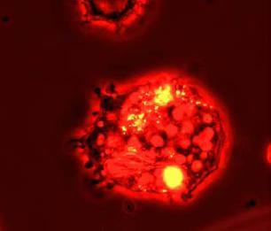
10 Healthcare: Cancer Cell Detection in Blood/Ear Tissue (Zharov Biris) What is new here Detection of a Single Cell in Blood


")
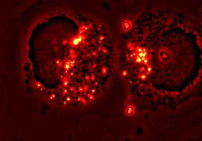
11 Healthcare: In Vivo Magnetic Enrichment & Photoacoustic Detection of Circulating Tumor (Zharov and Kim) Cells Magnet


12 Healthcare: Optical-Magnetic Nanoparticles for Cancer Treatment (Biris) What is new here: Exploding Cells under RF

13 Healthcare: Imaging Through Tissue InAs/InP/ZnSe Q-dots (Peng) CuInS 2 PL Intensity (a.u.) Wavelength (nm) What is new here flexible Infra-red emission ZnS InAs dots (NIR) in vivo imaging

")


14 Healthcare: Uptake and Clearing of CNTs by Lymph Vessel (Zharov & Biris) Raman Analysis 100µm Time 2 min Lymph Vessel Flow 100µm Time 12 min 100µm Fluorescent Dye Analysis 100µm 100µm Time 22 min Time 32 min What is new here CNT enter and propagate in Lymphatic


15 Healthcare: Graphitic Coated Magnetic Nanoparticles for Heating Cancer Cells with Radio Frequency (Biris) 5 n m What is new here Heating Cancer Cells with Radio Waves


16 Healthcare: In Vivo Nano-Thermolysis of Biological Tissues under Near-Infrared Laser Radiation (Biris & Boldor) What is new here Localized Thermal heating-cancer Tissue 16
 ZnSe")

 What is")


17 Energy Efficiency Nanoscale Materials (Peng) ZnSe Cu:ZnSe Mn:ZnSe Cu:ZnSe Emission PL Intensity (a.u.) Wavelength (nm) What is new here absorption /emission do not overlap & flexible emission Cu:ZnSe Mn:ZnSe Mn:ZnSe NN Labs our spin-off company

18 Energy Efficiency: Nanoscale Materials to Reduce Friction (Malshe) Novel Nano-Bio Materials that reduce friction in mechanical systems NanoGlide What is new here lowers friction better than anything else

19 Energy Efficiency: Nanoscale Materials with Large Thermo to Electric Conversion (Tchakhalian & Salamo) Devices that can convert wasted heat to electricity What is new here: Current Figure of merit is about ZT ~ 1. Our nanoscale oxide material is already about 1.5 and has potential to reach 3
 Hysteresis (Memory")

20 Energy Efficiency: Nanoscale Ferroelectrics (Bellaiche & Salamo) Hysteresis (Memory Element) BaTiO 3 Dots What is new here ferroelectric quantum dots form 10,000 times smaller memory

")

21 Renewable Energy: Novel Solar Cell Nanomaterial (Manasreh & Salamo) What is new here board band absorption for high efficiency
22 Impact in nanoscale materials and application Evidenced by: (NSF) Materials Research Science and Engineering Center (MRSEC) 6 spin-off companies with over 40 employees (Orlumet, Synanomet, Provectus, NNLabs, NanoMech, Nanoferr) State-of-the-art device fabrication facility, Authored some of the most compelling ideas in the field About 150 Publications with over 3000 Citations 32 Applied Physics Letters (APL) 12 Physical Review Letters (PRL) 2 Nature Materials 5 Nano Letters (NL) 6 Journal American Chemical Society (JACS) 5 Optics Letters (OL)
23 What s Next? Loadlock MBE Au Ga In E- Pulse To achieve arrays of Uniform QDs or QD molecules like never before GaAs-Buried InAs QDs To study plasmon Enhanced QD behaviors Complex of Au nanoparticle And InAs QDs Nanostructure complex Like never before Complex of GaAs nanowires And InAs QDs Arsenization and GaAs deposition In MBE chamber Au Deposition In NJP chamber GaAs deposition In MBE chamber

24 One Layer of Atoms at a Time Creates a New Material Never seen Before YBCO LCMO YBCO LCMO What is new here The data indicates a strong chemical bond between Cu and Mn and a new superconductor


25 Bone Regeneration (Biris & Jensen) Proportion of Medullary Canal filled by Endosteal New Bone Proportion Groups Hdroxy Apatite What is new here 43 human pre-clinical cases and 36 goat models

")


26 Nanostructural TiO 2 Nanotubes For Implant Coatings (Biris) TiO2 N2 O2 N2+O2 He Control N o. o f th e ce lls X Treatments O N What is new here TiO 2 enhances tissue regeneration

27 We Supplying Nanoscale Structures to many Research Organizations


28 The Future of Nanotechnology In Arkansas


29 & students for Nanoscience /depts/physics/

30 Specific Delivery of CNTs Time Dependence (Biris) What is new here DemonstratedCNT delivery to a Cancer Cell
31 Drug Delivery (Fologea & Borrelli) Scintillation Luminescence of Qdots X-ray radiation Key Ca Ca Ca Nanoparticle UV emission Caged Ca ions Freed Ca ions Ca Ca X-ray source targeting Qdots Activated Enzyme Cancer Drugs Loaded Liposome What is new here: Utilize X-ray absorbing Q -dots that emit UV light to release, caged Ca2+ ions, which activates an enzyme to open the liposome and release the drug.
 0.45 0.40 0.35 0.30 0.25 0.20 Absorbance 0 800 1000 1200 1400 1600 1800 2000 2200 Wavenumber (cm -1 ) 0.")
32 Tunable Infrared Photodetector (Manasreh) Bottom stack Top stack Semi-insulating GaAs Substrate Photoresponse (arbit units) T=7.0K SC-QWIP Vb=4.8V Vb=4.0V Vb=3.5V Vb=2.5V Absorbance (T=77K) Absorbance Wavenumber (cm -1 ) 0.15 What is new here voltage tunable color selection
33 Arkansas Nano Net
Spectra Chacracterizations of Optical Nanoparticles
 THAI NGUYEN UNIVERSITY OF EDUCATION Spectra Chacracterizations of Optical Nanoparticles Chu Viet Ha Department of Physics 18/2018 1 THAI NGUYEN UNIVERSITY OF EDUCATION Address 20 Luong Ngoc Quyen Street,
2.3 Quantum Dots (QDs)
") 2.3 Quantum Dots (QDs) QDs are inorganic nanocrystals, approximately 1 10 nm in size, with unique optical properties of broad excitation, narrow size-tunable emission spectra, high photochemical stability,
2.3 Quantum Dots (QDs) QDs are inorganic nanocrystals, approximately 1 10 nm in size, with unique optical properties of broad excitation, narrow size-tunable emission spectra, high photochemical stability,
EE 45X Biomedical Nanotechnology. Course Proposal
 EE 45X Biomedical Nanotechnology 1 Introduction Jie Chen ECERF W6-019 492-9820 jchen@ece.ualberta.ca Oct. 15, 2008 The purpose of this document is to propose a new course in the area of Biomedical Nanotechnology
Nanotechnology Principles, Applications, Careers, and Education. Copyright 2011 The Pennsylvania State University
 Nanotechnology Principles, Applications, Careers, and Education Copyright 2011 The Pennsylvania State University Outline What are the principles of nanotechnology? What are some applications? What kind
Quantum Dots and Carbon Nanotubes in Cancer diagnose EE453 Project Report submitted by Makram Abd El Qader
 Quantum Dots and Carbon Nanotubes in Cancer diagnose EE453 Project Report submitted by Makram Abd El Qader abdelqad@unlv.nevada.edu, Fall 2008 Abstract On the basis of research and cancer medical treatment,
Unit title: Nanotechnology
 Unit title: Nanotechnology Unit code: K/601/0311 QCF level: 4 Credit value: 15 Aim This unit examines the role of nanotechnology at the interface of Chemistry, Biology, Physics and Engineering, especially
Nanotechnology: The road for a better future. Prof. Uriel Levy
 Nanotechnology: The road for a better future Prof. Uriel Levy March 2016 The Nano-concept is in broad use but what is really Nano Science? Small is Different! Human Hair 100,000 smaller Molecule Nano size
Directed Assembly of Nanoparticles for Biosensing Applications
 NSF Nanoscale Science and Engineering Center for High-rate Nanomanufacturing (CHN) www.nano.neu.edu Directed Assembly of Nanoparticles for Biosensing Applications Ahmed Busnaina, Director, NSF Nanoscale
Nanotechnology for Next Generation Photovoltaics
 340 Nanotechnology for Next Generation Photovoltaics NARASIMHA RAO MAVILLA 1,2, CHETAN SINGH SOLANKI 1,3, JUZER VASI 1,2 * 1 National Centre for Photovoltaic Research & Education, IIT Bombay, Mumbai 400076,
ADVANCED NANOSCALE SCIENCE & ENGINEERING NANOPHYSICS SEMESTER MONTH CONTENT LAB THEMES SKILLS ASSESSMENTS. Cutting it Down to Nano Lab
 September Nano-Intro (Same topics for nanophysics and nanochem) Topic I: GOT NANO? Unit 1 Nano -Calculations Metric Review 2 Dimensional Analysis 3 Dimensional Analysis Sci. Not. & Sig. Figs. NanoDefinitions
Nanotechnology for Molecular and Cellular Manipulation
 Nanotechnology for Molecular and Cellular Manipulation Logan Liu Micro and Nano Technology Lab Department of Electrical & Computer Engineering University of Illinois Physical Systems Nano vs. Bio Micro
Multiphoton lithography based 3D micro/nano printing Dr Qin Hu
 Multiphoton lithography based 3D micro/nano printing Dr Qin Hu EPSRC Centre for Innovative Manufacturing in Additive Manufacturing University of Nottingham Multiphoton lithography Also known as direct
NANOTECHNOLOGY. I. Basic concept of Nanotechnology
 NANOTECHNOLOGY Girish N. Chaple Tushar P.Upalanchiwar 6 th Semister B.E 6 th SemisterB.E Department Of Electronics Engineering Department Of Electronics Engineering B.D.C.O.E Sevagram,Wardha B.D.C.O.E
Applications of Nanotechnology in Medical Device Design James Marti, Ph.D. Minnesota Nano Center
 Applications of Nanotechnology in Medical Device Design James Marti, Ph.D. Minnesota Nano Center November 4, 2015 The University of Minnesota Nano Center An open-use nanotechnology lab with tools for fabricating
Plasmonics using Metal Nanoparticles. Tammy K. Lee and Parama Pal ECE 580 Nano-Electro-Opto-Bio
 Plasmonics using Metal Nanoparticles Tammy K. Lee and Parama Pal ECE 580 Nano-Electro-Opto-Bio April 1, 2007 Motivation Why study plasmonics? Miniaturization of optics and photonics to subwavelength scales
CONTENTS. Introduction. NSOM Optical Fiber Probes
 CONTENTS Introduction NSOM Optical Fiber Probes AFM Probes AFM Probes Hard to achieve Force Constants and Resonance Frequencies Deep Trench AFM Probes Electrical and STM Probes Hollow AFM Nanopipette Probes
for Bioanalytical Applications
 Conferinţa Diaspora in Cercetarea Ştiinţifică şi Invăţămantul Superior din Romania Bucuresti, 21-24 Septembrie 2010 Multifunctional Plasmonic Nanosensors for Bioanalytical Applications Simion Astilean
The strategy. using Atomic Force Microscope; Biomolecules and Neutraceuticals examples
 The strategy for Bionanomolecules Characterizations using Atomic Force Microscope; Biomolecules and Neutraceuticals examples Dr. NagibAli Elmarzugi, PhD Head of Nanotechnology Research gp., Biotechnology
Nanotechnology. DTSC and Nanotechnology
 1 of 5 6/3/2010 10:16 AM Nanotechnology DTSC and Nanotechnology Nanotechnology is a science that promises breakthroughs in all kinds of areas. We are already seeing it in stain resistant clothes, stronger
Nanotechnology Solutions for Energy
 Nanotechnology Solutions for Energy - Innovation and Sustainable Development with nanotechnology - Professor Rüdiger Iden Polymer Research BASF Aktiengesellschaft Definition Nanotechnology We define nanoscience
NRL Institute for Nanoscience 1 May 2012
 NRL Institute for Nanoscience 1 May 2012 Dr. Eric S. Snow, Director The Naval Research Laboratory Highly interdisciplinary laboratory Research Focus Areas Battlespace Environments, Undersea Warfare, Space
Physics and Material Science of Semiconductor Nanostructures
 Physics and Material Science of Semiconductor Nanostructures PHYS 570P Prof. Oana Malis Email: omalis@purdue.edu Lecture 6 Bulk semiconductor growth Single crystal techniques Nanostructure fabrication
WHAT DO WE MEAN BY NANOSCIENCE OR NANOTECHNOLOGY EDUCATION?
 2nd US-Korea NanoForum, Los Angeles, USA, February 17-19, 2005 WHAT DO WE MEAN BY NANOSCIENCE OR NANOTECHNOLOGY EDUCATION? Donald R. Baer Pacific Northwest National Laboratory don.baer@pnl.gov Talk intended
Structure and optical properties of M/ZnO (M=Au, Cu, Pt) nanocomposites
 nanocomposites") Solar Energy Materials & Solar Cells 8 () 339 38 Structure and optical properties of M/ (M=Au, Cu, Pt) nanocomposites U. Pal a,b, *, J. Garc!ıa-Serrano a, G. Casarrubias-Segura a, N. Koshizaki c, T. Sasaki
Solar Energy Materials & Solar Cells 8 () 339 38 Structure and optical properties of M/ (M=Au, Cu, Pt) nanocomposites U. Pal a,b, *, J. Garc!ıa-Serrano a, G. Casarrubias-Segura a, N. Koshizaki c, T. Sasaki
Center for Integrated Nanotechnologies & Semiconducting Nanowires
 Center for Integrated Nanotechnologies & Semiconducting Nanowires S. Tom Picraux Chief Scientist Center for Integrated Nanotechnologies picraux@lanl.gov Arizona Nanotechnology: Small is Big April 10, 2008
The California Nanosystems Institute
 The California Nanosystems Institute Evelyn L. Hu Acting Director, California NanoSystems Institute University of California at Santa Barbara California NanoSystems Institute A Vision for the Future 50
Tunable Nanoscale Plasmon Antenna for Localization and Enhancement of Optical Energy. Douglas Howe
 Tunable Nanoscale Plasmon Antenna for Localization and Enhancement of Optical Energy Douglas Howe Applied Optics Spring 2008 Table of Contents Abstract... 3 Introduction... 4 Surface Plasmons... 4 Nano
ANU.
 Solar @ ANU http://sun.anu.edu.au/ Global Solar Sales Industry doubling times 20 months 30 months Source: Photon International Worldwide solar Severe industry shakeout ¾ of companies are folding PV production
Contents Preface xiii Introduction Fabrication and manufacturing technology for optical MEMS
 Contents Preface xiii 1 Introduction 1 1.1 Optical MEMS and optofluidics 1 1.2 History 1 1.2.1 Processes and materials 1 1.2.2 Early devices and systems 2 1.3 Progress in optical MEMS and optofluidics
Laser treatment of gravure-printed ITO films on PET
 Laser treatment of gravure-printed ITO films on PET Howard V Snelling, Anton A Serkov, Jack Eden, Rob J Farley Physics, School of Mathematical and Physical Sciences, University of Hull, HU6 7RX, UK Presentation
Workshop on Nanoscience and Catalysts March 2008, QAU, Islamabad Nanocomposites for Thermal management Applications
 Fazal Ahmad Khalid Pro-Rector GIK Institute of Engineering Sciences and Technology Topi, NWFP, Pakistan (Khalid@giki.edu.pk) Workshop on Nanoscience and Catalysts 24-25 March 2008, QAU, Islamabad Nanocomposites
ENS 06 Paris, France, December 2006
 CARBON NANOTUBE ARRAY VIAS FOR INTERCONNECT APPLICATIONS Jyh-Hua ng 1, Ching-Chieh Chiu 2, Fuang-Yuan Huang 2 1 National Nano Device Laboratories, No.26, Prosperity Road I, Science-Based Industrial Park,
Dielectric II-VI and IV-VI Metal Chalcogenide Thin Films in Hollow Glass Waveguides (HGWs) for Infrared Spectroscopy and Laser Delivery
 for Infrared Spectroscopy and Laser Delivery") Dielectric II-VI and IV-VI Metal Chalcogenide Thin Films in Hollow Glass Waveguides (HGWs) for Infrared Spectroscopy and Laser Delivery Carlos M. Bledt * a, Daniel V. Kopp a, and James A. Harrington a
Dielectric II-VI and IV-VI Metal Chalcogenide Thin Films in Hollow Glass Waveguides (HGWs) for Infrared Spectroscopy and Laser Delivery Carlos M. Bledt * a, Daniel V. Kopp a, and James A. Harrington a
Future Areas of Technology Convergence
 Future Areas of Technology Convergence Dr J Malcolm Wilkinson Managing Director Technology For Industry Ltd Cambridgeshire, UK Medilink Yorkshire & Humberside, 8 December 2005 1 Technology For Industry
CHAPTER 8 CONCLUSIONS AND SCOPE FOR FUTURE WORK
 CHAPTER 8 CONCLUSIONS AND SCOPE FOR FUTURE WORK In this thesis an experimental investigation about Magnisium oxide (MgO) nanoparticles and its nanocomposites i.e.mgo-x (X= NiO, CuO, Co3O4, Fe2O3, CeO2,
Electricity from the Sun (photovoltaics)
") Electricity from the Sun (photovoltaics) 0.4 TW US Electricity Consumption 100 100 square kilometers of solar cells could produce all the electricity for the US. But they are still too costly. The required
Electricity from the Sun (photovoltaics) 0.4 TW US Electricity Consumption 100 100 square kilometers of solar cells could produce all the electricity for the US. But they are still too costly. The required
Fe doped Magnetic Nanodiamonds made by Ion
 Fe doped Magnetic Nanodiamonds made by Ion Implantation ChienHsu Chen a, I.C. Cho b, Hui-Shan Jian c and H. Niu a* a Nuclear Science and Technology Development Center, National Tsing Hua University, HsinChu
Thermal Annealing Effects on the Thermoelectric and Optical Properties of SiO 2 /SiO 2 +Au Multilayer Thin Films
 American Journal of Materials Science 2015, 5(3A): 31-35 DOI: 10.5923/s.materials.201502.05 Thermal Annealing Effects on the Thermoelectric and Optical Properties of SiO 2 /SiO 2 +Au Multilayer Thin Films
LOW TEMPERATURE PHOTONIC SINTERING FOR PRINTED ELECTRONICS. Dr. Saad Ahmed XENON Corporation November 19, 2015
 LOW TEMPERATURE PHOTONIC SINTERING FOR PRINTED ELECTRONICS Dr. Saad Ahmed XENON Corporation November 19, 2015 Topics Introduction to Pulsed Light Photonic sintering for Printed Electronics R&D Tools for
Simple fabrication of highly ordered AAO nanotubes
 Journal of Optoelectronic and Biomedical Materials Volume 1, Issue 1, March 2009, p. 79-84 Simple fabrication of highly ordered AAO nanotubes N. Taşaltin a, S. Öztürk a, H. Yüzer b, Z. Z. Öztürk a,b* a
Research seminar Solar energy harvesting with the application of nanotechnology
 Research seminar Solar energy harvesting with the application of nanotechnology By B.GOLDVIN SUGIRTHA DHAS, AP/EEE SNS COLLEGE OF ENGINEERING, Coimbatore Objective By 2050 30 TW The fossil fuels will exhausted
SUPPLEMENTARY INFORMATION
 Supplementary Figures SUPPLEMENTARY INFORMATION Supplementary Figure S1. Schematic Representation of temperature-controlled sonication apparatus. 1 Solution Abs (a.u.) 0.18 HiPco SWNT Dispersion in rr-p3ddt/toluene
Red luminescence from Si quantum dots embedded in SiO x films grown with controlled stoichiometry
 Red luminescence from Si quantum dots embedded in films grown with controlled stoichiometry Zhitao Kang, Brannon Arnold, Christopher Summers, Brent Wagner Georgia Institute of Technology, Atlanta, GA 30332
HYPERSPECTRAL MICROSCOPE PLATFORM FOR HIGHLY MULTIPLEX BIOLOGICAL IMAGING. Marc Verhaegen
 HYPERSPECTRAL MICROSCOPE PLATFORM FOR HIGHLY MULTIPLEX BIOLOGICAL IMAGING Marc Verhaegen CMCS, MONTREAL, MAY 11 th, 2017 OVERVIEW Hyperspectral Imaging Multiplex Biological Imaging Multiplex Single Particle
Nano Fabrication Research at FIU
 Nano Fabrication Research at FIU Professor W. Choi s Nano Materials and Devices Lab FIU logo with 25nm line width by e-beam lithography Fastest growing University in the US- Ranked in top 25 largest Universities
In Vivo Applications of Near-Infrared Quantum Dots
 In Vivo Applications of Near-Infrared Quantum Dots John V. Frangioni, M.D., Ph.D. Assistant Professor of Medicine Assistant Professor of Radiology Harvard Medical School Moungi G. Bawendi, Ph.D. Professor
Nanotechnology Activities in Korea
 Nanotechnology Activities in Korea Hee-Gook Lee President LG Electronics, Inc. CONTENTS I. National Programs Industry Academia NTRA II. Summaries Overview of Korean Approach Korean environments and the
Performance and Radiation Resistance of Quantum Dot Multi-Junction Solar Cells
 B.C. Richards 1, Young Lin 1, Pravin Patel 1, Daniel Chumney 1, Paul R. Sharps 1 Chris Kerestes 1,2, David Forbes 2, Kristina Driscoll 2, Adam Podell 2, Seth Hubbard 2 1 EMCORE Corporation, Albuquerque,
IMRE/ETPL Flagship Project
 IMRE/ETPL Flagship Project Nanoparticulate Barrier Films & Gas Permeation Measurement Techniques for Thin Film Solar & Display Application Problems Senthil Ramadas Institute of Materials Research & Engineering
Engineering Quantum Dots for Live-Cell Single-Molecule Imaging
 Engineering Quantum Dots for Live-Cell Single-Molecule Imaging Andrew M. Smith and Shuming Nie Georgia Tech and Emory University Department of Biomedical Engineering 2011 NSF Nanoscale Science and Engineering
Supporting Information for
 Electronic Supplementary Material (ESI) for Nanoscale. This journal is The Royal Society of Chemistry 2015 Supporting Information for Large-Scale Freestanding Nanometer-thick Graphite Pellicle for Mass
Atomic Layer Deposition (ALD)
") Atomic Layer Deposition (ALD) ALD provides Uniform, controlled, conformal deposition of oxide, nitride, and metal thin films on a nanometer scale. ALD is a self limiting thin film deposition technique
Atomic Layer Deposition (ALD) ALD provides Uniform, controlled, conformal deposition of oxide, nitride, and metal thin films on a nanometer scale. ALD is a self limiting thin film deposition technique
Nanomaterials as Transducers in Biosensors. Nanotechnology. Nanotechnology Areas for Development. The Nanotechnology Development Stages
 University of Crete Department of Chemistry Laboratory of Analytical Chemistry Iraklion, Crete, GREECE URL: www.analytical_chemistry.uoc.gr Nanomaterials as Transducers in Biosensors.. Chaired by: Dr Renzo
Carbon Nanotube Material Quality Assessment
 Carbon Nanotube Material Quality Assessment Sivaram Arepalli 1, Edward Sosa 1, Pasha Nikolaev 1, William Holmes 1, Olga Gorelik 1, and Leonard Yowell 2 1 ERC Inc. / NASA - Johnson Space Center, Houston,
Latest Solar Technologies
 Latest Solar Technologies Mrs. Jothy.M. Saji Mrs. Sarika. A. Korade Lecturer Lecturer IE Dept, V.P.M s Polytechnic, Thane IE Dept, V.P.M s Polytechnic, Thane Mob no. : 9892430301 Mob no. : 9960196179 Email:
STUDY OF NANO DEVICE FOR EFFECTIVE DETECTION, DIAGNOSIS AND TREATMENT OF CANCER
 STUDY OF NANO DEVICE FOR EFFECTIVE DETECTION, DIAGNOSIS AND TREATMENT OF CANCER 1 E.N.Ganesh, 2 R.Kaushik Ragavan, 3 Bandyopadhyay Arka Prava 4 M. Krishna Kumar 1 Professor, Rajalakshmi Engineering College,
Towards scalable fabrication of high efficiency polymer solar cells
 Towards scalable fabrication of high efficiency polymer solar cells Hui Joon Park 2*, Myung-Gyu Kang 1**, Se Hyun Ahn 3, Moon Kyu Kang 1, and L. Jay Guo 1,2,3 1 Department of Electrical Engineering and
Supplementary Information
 Supplementary Information Supplementary Figure 1 Characterization of precursor coated on salt template. (a) SEM image of Mo precursor coated on NaCl. Scale bar, 50 μm. (b) EDS of Mo precursor coated on
III-V heterostructure TFETs integrated on silicon for low-power electronics
 In the Quest of Zero Power: Energy Efficient Computing Devices and Circuits III-V heterostructure TFETs integrated on silicon for low-power electronics K. E. Moselund, M. Borg, H. Schmid, D. Cutaia and
Fabrication of Highly Ordered Al 2 O 3 Nanohole Arrays As a Nanostructured Template
 Fabrication of Highly Ordered Al 2 O 3 Nanohole Arrays As a Nanostructured Template Jie Gong, Bill Butler and Giovanni Zangari Materials Science Program University of Alabama at Tuscaloosa This work was
Autocloning FIGURE 5 AUTOCLONED CRYSTAL STRUCTURE Holographic Lithography Multibeam Interference Lithography...
 CHAPTER ONE: INTRODUCTION... 1 STUDY BACKGROUND... 1 STUDY GOALS AND OBJECTIVES... 1 INTENDED AUDIENCE... 1 SCOPE AND FORMAT... 2 METHODOLOGY AND INFORMATION SOURCES... 2 ANALYST CREDENTIALS... 3 RELATED
Photonic Drying Pulsed Light as a low Temperature Sintering Process
 Photonic Drying Pulsed Light as a low Temperature Sintering Process Lou Panico Xenon Corporation W E S T E R N M I C H I G A N U N I V E R S I T Y PRESENTATION OVERVIEW What is Printed Electronics Materials
Moving toward Sustainability
 Nanotechnology and the Environment: Moving toward Sustainability Barbara Karn, PhD Health and Environment Organization April 17, 2012 A bit of history Nanotechnology is enabled Nanotechnology is recognized
Nanodiamond-Polymer Composite Fibers and Coatings
 Nanodiamond-Polymer Composite Fibers and Coatings Yury Gogotsi et al. A.J. Drexel Nanotechnology Institute and Department of Materials Science and Engineering Drexel University, Philadelphia, Pennsylvania
Nanotechnology in the Treatment of Cancer
 Page 1 of 11 Nanotechnology in the Treatment of Cancer What is Nanotechnology The term Nanotechnology originates from the Greek word meaning dwarf. The scale of nanotechnology puts into perspective how
30: More Nano & Semiconductors
 30: More Nano & Semiconductors Nanotechnology Con't Biology at the Nanoscale Some Applications Are there any concerns? Reading: Ch 24.22-24.30 Ch 8.16-8.17 Ch 3.19-3.20 More Semiconductors Band Theory
ECE280: Nano-Plasmonics and Its Applications. Week5. Extraordinary Optical Transmission (EOT)
") ECE280: Nano-Plasmonics and Its Applications Week5 Extraordinary Optical Transmission (EOT) Introduction Sub-wavelength apertures in metal films provide light confinement beyond the fundamental diffraction
ECE280: Nano-Plasmonics and Its Applications Week5 Extraordinary Optical Transmission (EOT) Introduction Sub-wavelength apertures in metal films provide light confinement beyond the fundamental diffraction
Application of sprayed carbon nanotubes to light detectors
 Olive Tree (St. Nicholas Church in Bari) Application of sprayed carbon nanotubes to light detectors Valentini A. (1)(2), Melisi D. (1), Valentini M. (1), Nitti M.A. (2), Biagi P.F. (2) (1) INFN Sezione
Nanotechnology: Balancing Benefits and Risks. Kristen M. Kulinowski, PhD Rice University September 7, 2006
 Nanotechnology: Balancing Benefits and Risks Kristen M. Kulinowski, PhD Rice University September 7, 2006 What is Nanotechnology? Nanotechnology is the understanding and control of matter at dimensions
Synthesis and Characterization of Cadmium Sulfide (CdS) Quantum Dots (QDS) for Quantum Dot Sensitized Solar Cell Applications
 Quantum Dots (QDS) for Quantum Dot Sensitized Solar Cell Applications") Nano Vision, Vol. 5(7-9), 237-241, July-September 2015 (An International Research Journal of Nano Science & Technology), www.nano-journal.org ISSN 2231-2579 (Print) ISSN 2319-7633 (Online) Synthesis and
Nano Vision, Vol. 5(7-9), 237-241, July-September 2015 (An International Research Journal of Nano Science & Technology), www.nano-journal.org ISSN 2231-2579 (Print) ISSN 2319-7633 (Online) Synthesis and
INTRODUCTION TO NANOSCALE SCIENCE & ENGINEERING NANOPHYSICS SEMESTER MONTH CONTENT LAB THEMES SKILLS ASSESSMENTS. Math Tool Kit
 September Nano-Intro (Same topics for nanophysics and nanochem) Topic I: NAN-OH!! WHAT? Unit 1 Nano -The Unit SI System of Units Unit Conversions Intro to NanoBook NanoDefinitions Scaling from Macro to
Supplementary Figure S1 Photograph of MoS 2 and WS 2 flakes exfoliated by different metal naphthalenide (metal = Na, K, Li), and dispersed in water.
, and dispersed in water.") Supplementary Figure S1 Photograph of MoS 2 and WS 2 flakes exfoliated by different metal naphthalenide (metal = Na, K, Li), and dispersed in water. Supplementary Figure S2 AFM measurement of typical LTMDs
Supplementary Figure S1 Photograph of MoS 2 and WS 2 flakes exfoliated by different metal naphthalenide (metal = Na, K, Li), and dispersed in water. Supplementary Figure S2 AFM measurement of typical LTMDs
BIOSENOSRS BIO 580. Nanobiosensors WEEK-13 Fall Semester. Faculty: Dr. Javed H. Niazi KM Faculty of Engineering & Natural Sciences Sabanci University
 BIOSENOSRS BIO 580 Nanobiosensors WEEK-13 Fall Semester Faculty: Dr. Javed H. Niazi KM Faculty of Engineering & Natural Sciences Sabanci University Topics that will be covered in the course History of
White Paper: Pixelligent Zirconia Nanocrystals for OLED Applications
 Zhiyun (Gene) Chen, Ph.D., Vice President of Engineering Pixelligent Technologies LLC, 6411 Beckley Street, Baltimore, Maryland 21224 Email: zchen@pixelligent.com September 2014 Background The past few
IJSER. Nanotechnology is the creation of functional 1. INTRODUCTION TO NANOTECHNOLOGY 2. INTERDISCIPLANRY APPROACH TO NANOTECHNOLOGY
 International Journal of Scientific & Engineering Research, Volume 4, Issue 12, December-2013 1314 Integrative Approach of Nanotechnology Akash Pardeshi 1, Nilanshu Ramteke 2 1 B.E, Medi-caps Institute
MODERN COMPUTER TENDING TOWARDS NANOTECHNOLOGY MAKING GRATE GROWTH IN 21 ST CENTURY
 MODERN COMPUTER TENDING TOWARDS NANOTECHNOLOGY MAKING GRATE GROWTH IN 21 ST CENTURY Mrs. Jayashree Yadannavar Department of Information Technology,MIT AOE, Alandi(D),Pune ABSTRACT At present in the field
Department of Chemistry, University of California, Davis, California 95616, USA 2
 Enhance Solar Water Splitting Performance by Utilizing Near Infrared Radiation with Composite Films of Hematite and Rare Earth Doped Upconversion Materials Ming Zhang, 1 Yongjing Lin, 2 Thomas J. Mullen,
Dr. Arun Singh. Sponsored by DST. Year of start. Held. Principal Investigator. Principal Investigator BOYSCAST FELLOW
 Dr. Arun Singh Advanced Electronic and Nano-Materials Laboratory R.N.- 304 III Floor, Department of Physics Faculty of Natural Sciences Jamia Millia Islamia, Central University, New Delhi-110025 (INDIA).
Nanotechnology Program Elements. Nanoelectronics and Computing. Sensors. - Structural Materials. Structural Materials
 Nanotechnology Program Elements - Nanoelectronics and Computing - Sensors - Structural Materials Nanoelectronics and Computing Molecular electronics & photonics Computing architecture Assembly Sensors
Studies on Structural and Optical Properties of Iron doped Cds Nanoparticles ABSTRACT
 Studies on Structural and Optical Properties of Iron doped Cds Nanoparticles Atheek P., Vidhya M. and Balasundaram O. N Department of Physics, PSG College of Arts & Science, Coimbatore, Tamil Nadu, India
Welcome to Nanotechnology Spin-a-Prize, a game show about nanoscale science, engineering, and technology! My name is and I ll be your host.
 Welcome to Nanotechnology Spin-a-Prize, a game show about nanoscale science, engineering, and technology! My name is and I ll be your host. Nanotechnology Spin-a-Prize consists of two rounds. Before each
Supplementary Figures
 Supplementary Figures Supplementary Figur e 1. DLS analyses of DSPE PEG 2000 Amine DC(8,9)PC LM (a) immediately after its preparation and (b) after 3 days. Supplementary Figure 2. Particle size distribution
Motivation: Biofunctional Composite Nanoparticles
 1 Motivation: Biofunctional Composite Nanoparticles Iron Oxide Core Magnetic core Alternating magnetic field Brownian and Neél relaxation Bi-Material Composites MRI contrast enhancement and RF thermal
NINT Supporting Innovative Ideas through Nanotechnology
 NINT Supporting Innovative Ideas through Nanotechnology (Capabilities and Expertise) Dr. Marianna Kulka, PhD Group Leader, NINT National Research Council Marianna.kulka@nrc.ca National Institute for Nanotechnology
CURRICULUM VITAE. Solid State Physics (PG-II) ACADEMIC AWARDS:
 ACADEMIC AWARDS:") Dr. RABINDRA NATH GAYEN Assistant Professor Department of Physics Presidency University 86/1 College Street Kolkata - 700073. e-mail: rabin.physics@presiuniv.ac.in rabin.gayen@gmail.com Phone No: +91-9836754743
Dr. RABINDRA NATH GAYEN Assistant Professor Department of Physics Presidency University 86/1 College Street Kolkata - 700073. e-mail: rabin.physics@presiuniv.ac.in rabin.gayen@gmail.com Phone No: +91-9836754743
Photoluminescence Spectroscopy on Chemically Synthesized Nanoparticles
 Photoluminescence Spectroscopy on Chemically Synthesized Nanoparticles Torben Menke 1 Institut für Angewandte Physik und Zentrum für Mikrostrukturforschung Universität Hamburg Diploma Talk, 18.12.27 1
Nanomaterials and Analytics Semiconductor Nanocrystals and Carbon Nanotubes. - Introduction and Preparation - Characterisation - Applications
 Nanomaterials and Analytics Semiconductor Nanocrystals and Carbon Nanotubes - Introduction and Preparation - Characterisation - Applications Simple molecules
Photonic Sintering of Silver for Roll-to-Roll Printed Electronics. Saad Ahmed, PhD Manager-Engineering
 Photonic Sintering of Silver for Roll-to-Roll Printed Electronics Saad Ahmed, PhD Manager-Engineering Topics Introduction Significance of nanotechnology Conductive inks Pulsed light for sintering Reel-to-reel
Nanomaterials for Healthcare. Hans Hofstraat. hilips Research Laboratories, Eindhoven, The Netherlands
 Nanomaterials for Healthcare Hans Hofstraat hilips Research Laboratories, Eindhoven, The Netherlands utline Introduction Promises of nanotechnology Nanotechnology at Philips Using nanotechnology for real
Nanotechnology and the Environment: Benefits and Risks. Kristen M. Kulinowski, PhD
 Nanotechnology and the Environment: Benefits and Risks Kristen M. Kulinowski, PhD kk@rice.edu Center for Biological & Environmental Nanotechnology Research Education Outreach Pd + Functional Nanoparticle
Chapter 7 NANOIMPRINTED CIRCULAR GRATING DISTRIBUTED FEEDBACK DYE LASER
 Chapter 7 66 NANOIMPRINTED CIRCULAR GRATING DISTRIBUTED FEEDBACK DYE LASER 7.1 Introduction In recent years, polymer dye lasers have attracted much attention due to their low-cost processing, wide choice
Nanotechnology. from small dimensions to big business Thomas Liljenberg, Olof Hjortstam, Silvia Volponi
 Nanotechnology from small dimensions to big business Thomas Liljenberg, Olof Hjortstam, Silvia Volponi Nanotechnology. It is difficult to overstate the potential of this newcomer to the technology world,
Glossary of Terms Specific to the general field of Light Therapy
 Glossary of Terms Specific to the general field of Light Therapy Absorption When light quanta travel through tissue, the energy is eventually absorbed by some component within the tissue. When energy is
University of Groningen
 University of Groningen Revealing the interparticle magnetic interactions of iron oxide nanoparticles-carbon nanotubes hybrid materials Douvalis, A.P.; Georgakilas, V.; Tsoufis, T.; Gournis, D.; Kooi,
New generation of solar cell technologies
 New generation of solar cell technologies Emerging technologies and their impact on the society 9th March 2017 Dhayalan Velauthapillai Professor, Faculty of Engineering and Business Administration Campus
Deliverable D1.4: Report on QDs with tunable color and high quantum yield. Summary
 Deliverable D.4: Report on QDs with tunable color and high quantum yield Responsible author: Dr Beata Kardynal, FZJ Summary The synthesis of the InP/ZnS nanocrystals with wavelengtnh in the range of green
Outline 4/25/2013. Titanium Dioxide Pigment and Nano Grades. Disclaimer
 Titanium Dioxide Pigment and Nano Grades Chris DeMerlis Colorcon, Inc. April 29, 2013 Disclaimer This presentation reports on work completed by Chris DeMerlis in support of IPEC and IACM and does not necessarily
Journal of Chemical and Pharmaceutical Research, 2017, 9(1): Research Article
: Research Article") Available online www.jocpr.com Journal of Chemical and Pharmaceutical Research, 2017, 9(1):163-167 Research Article ISSN : 0975-7384 CODEN(USA) : JCPRC5 Synthesis and Characterization of Carbon Nano Spheres
Available online www.jocpr.com Journal of Chemical and Pharmaceutical Research, 2017, 9(1):163-167 Research Article ISSN : 0975-7384 CODEN(USA) : JCPRC5 Synthesis and Characterization of Carbon Nano Spheres
Title: Localized surface plasmon resonance of metal nanodot and nanowire arrays studied by far-field and near-field optical microscopy
 Contract Number: AOARD-06-4074 Principal Investigator: Heh-Nan Lin Address: Department of Materials Science and Engineering, National Tsing Hua University, 101, Sec. 2, Kuang Fu Rd., Hsinchu 30013, Taiwan
Synthesis processes of materials for quantum technologies: diamond and oxide films
 Texte Synthesis processes of materials for quantum technologies: diamond and oxide films Alexandre Tallaire, Alban Ferrier, Diana Serrano, Philippe Goldner IRCP, Chimie ParisTech Ovidiu Brinza, Vianney