High Speed Serial Link (HSSL) Channel Modeling. CST workshop series 2010 February 10 1
|
|
|
- Sheryl Young
- 6 years ago
- Views:
Transcription

1 High Speed Serial Link (HSSL) Channel Modeling CST workshop series 2010 February 10 1
2 Outline Introduction HSSL design workflow Creating a HSSL model Simulating a HSSL HSSL modeling example CST workshop series 2010 February 10 2


 Rx www.")
3 Introduction The challenge: Send a data stream from a Tx to a Rx at a given data rate while meeting voltage and timing constraints (eye height and width) Tx Copper traces Main interconnect Multilayer PCB Vref Rx en Tx On-package interconnect - Escape - Main TL On-package vias -PTH -uvias On-board interconnect -MS -SL On-board vias -blind -buried Pkg. to board transition (socket) Rx CST workshop series 2010 February 10 3


4 Introduction Signal integrity issues and considerations: Dielectric Losses Copper Roughness Skin Effect Parasitic modes Signal Degradation Radiation Cross-talk Reflections Need modeling tools which account for physical effects in order to make realistic predictions, 3D Field Full Wave simulators a must Accurate models needed for accurate predictions CST MWS, Full wave physics and accuracy requirements CST workshop series 2010 February 10 4
5 HSSL analysis workflow Workflow and integration Pre and post layout analysis Time and frequency domain solutions S-parameters, Crosstalk analysis, TDR, Eye diagrams Performance SPICE models extraction Circuit EM co-simulation Full channel characterization IBIS and non-linear models CST workshop series 2010 February 10 5


6 HSSL analysis workflow: Pre-layout Approach: Build and cascade segmented models High Speed connector Diff. Pkg. vertical transition Import model from CAD tool if available Create 3D model using MWS s powerful GUI Simulate using Time or Frequency domain solver Create an S-parameter model Synthesize an equivalent circuit using MOR CST workshop series 2010 February 10 6 Socket model


7 HSSL analysis workflow: Pre-layout Design of package and PCB vias plays an important role Standard method: Edit and extract from Layout - Time consuming - Lack of parameterization CST Via Wizard Macro enabled Spreadsheet based High flexibility Full parameterization Automatic port definition CST workshop series 2010 February 10 7
 Excellent approach for analysis of interconnect length and data rate scalability")
 Transient or Frequency domain simulators Active (IBIS, Spice Netlist, etc.")
8 HSSL analysis workflow: Pre-layout Cascading the segmented models in CST DESIGN STUDIO: CST MWS TS TS CST DS (coupled SL) TS At pre-layout stage, common approach is to use 2D models for main High speed interconnect (SL, MS) Excellent approach for analysis of interconnect length and data rate scalability Straightforward cascading of segmented models Multiple formats supported (Spice, HSpice, TS, etc.) Transient or Frequency domain simulators Active (IBIS, Spice Netlist, etc.) and passive components Optimization/parameter sweep Co-simulation with CST MWS Included with standard license CST workshop series 2010 February 10 8
 2.")
 Self cleaning process Pre-mesh definition Discrete components Stack-up definition Materials definition")
9 HSSL analysis workflow: Post-layout A segmented model approach is also a common practice: Extract vias and high speed interconnect models from layout database CST MWS and EDA links 1. Cadence Allegro ( *.brd, *.mcm) 2. Mentor Graphic ( Expedition and Board Station) 3. Zuken 4. ODB++ 5. Gerber ( single/multiple layer) 6. Dxf ( import/export) Self cleaning process Pre-mesh definition Discrete components Stack-up definition Materials definition CST workshop series 2010 February 10 9

10 Powerful EDA interface Customized extraction Area selection Net selection + surrounding area CST workshop series 2010 February 10 10


11 Easy Merging of imported components PCB + package uvw on specific net CST workshop series 2010 February 10 11


12 Post-Layout: Pkg+PCB channel Large HSSL channel modeling example Time domain solver Fast and memory efficient, enables large model simulations High performance computing options available (GPU, MPI, DC) Single vs. multiple simulations and cascading CST workshop series 2010 February 10 12


13 Simulating a High Speed Serial Link Frequency domain simulation SE/Mixed-mode converter RL IL Next Fext CST workshop series 2010 February 10 13
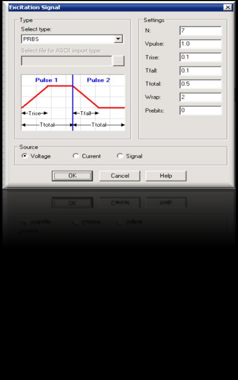

14 Simulating a High Speed Serial Link Time domain simulation Next CST workshop series 2010 February Fext


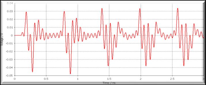
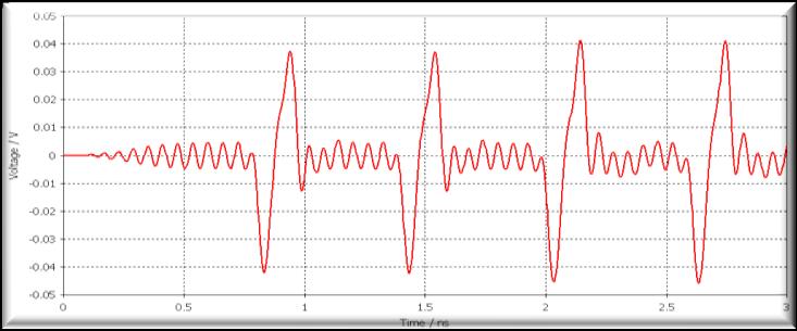
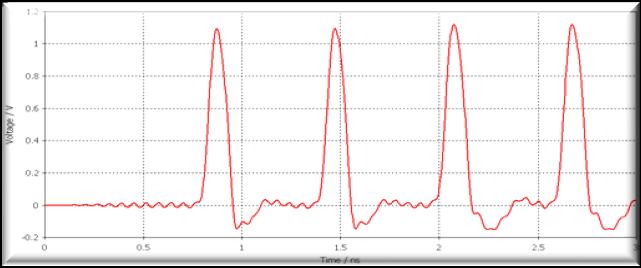
15 Simulating a High Speed Serial Link Time domain simulation (Eye Diagram calculation) Tx Channel Rx CST workshop series 2010 February 10 15


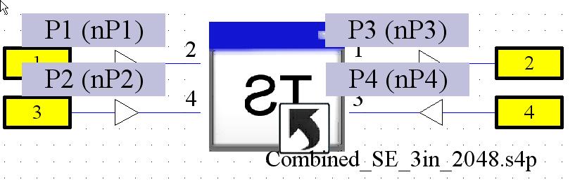
16 Demo: Chip-to-chip communication Segmentation lines Main interconnect (SL) PCB Via 2 Package 1 PCB Via 1 Package 2 Package Details PCB Transition Details CST workshop series 2010 February 10 16

17 Realistic Example: Package 2 Package 1 CST workshop series 2010 February layer PCB: FR4 Package1: 12-layer organic Package2: 21-layer ceramic


18 Structure of the Entire Channel Pkg 1 PCB Interconnect AC Caps Pkg 2 CST workshop series 2010 February 10 18
19 High-Speed Channel Modeling and Correlation Package 1 modeling Package 2 modeling PCB modeling Entire channel modeling Measurement and correlation CST workshop series 2010 February 10 19


20 Modeling Package 1 CST Links Automatic CST-Cadence Translator A section of the package is extracted via CST Links CST workshop series 2010 February Package details


21 Modeling Package 1 (Cont d) Package top port2 port4 Package interconnect port1 port3 Details of package 1 simulated net and port definition CST workshop series 2010 February Package vertical transition
 time Memory usage 12GB 32h (no GPU) www.cst.")
22 Package 1: Simulation Results in output Simulation approach: TD based on Finite Integration Technique Excite each port with a Gaussian signal with spectral content of interest (40GHz) Capture time signatures at each port Fourier transform to obtain S-parameters NEXT FEXT Run-time statistics: Mesh cells 5.5M Simulation 8h (with GPU) time Memory usage 12GB 32h (no GPU) CST workshop series 2010 February 10 22


23 Modeling Package 2 Net extracted via CST Links WG ports details: Bottom Top Extrude signal and GND pads CST workshop series 2010 February 10 23
24 Simulated Differential S-Parameters - Very low differential Insertion Loss (~7dB at 40GHz) CST workshop series 2010 February 10 24

25 Modeling the Entire Channel 1 2 Model 1 (P1) Model 2 (PCB) Model 3 (P2) 3 4 Simulated Single-Ended S-Parameters CST workshop series 2010 February 10 25

26 Measurement Setup for the Entire Channel Probe 1 300um pitch probe Package1 Package2 200um pitch probe Probe 3 CST workshop series 2010 February 10 26
27 Comparison between Simulation and Measurement Simulation Measurement Very good correlation between simulation and measurement CST workshop series 2010 February 10 27
28 Conclusions A workflow for the design of HSSL was presented Powerful integration between CST MWS and CST DS Pre- and post- layout capabilities discussed CST MWS provides fast and accurate characterization of HSSL passive component CST DS enables full HSSL link simulation A practical example was presented CST workshop series 2010 February 10 28
NI AWR Design Environment V14
 Product Review NI AWR Design Environment V14 Accelerating RF/Microwave Design From Concept to Product Advancing communication and sensor technologies, driven by applications such as 5G, internet of things
Xpedition Package Integrator
 Xpedition Package Integrator Xpedition D A T A S H E E T FEATURES AND BENEFITS: Figure 1: The Xpedition Package Integrator Flow comprises all the tools necessary for efficient package/pcb codesign, for
Signal & Power Integrity Analysis Services for Test boards
 Caliber Interconnect Solutions Design for perfection Signal & Power Integrity Analysis Services for Test boards Caliber Interconnect Solutions (Pvt) Ltd No 6,1 st Street Gandhi Nagar, Kavundampalayam,
If you want then let us introduce you to CADSTAR. The most powerful price/performance solution for PCB design
 Powerful PCB Design If you want... The most powerful price/performance solution for PCB design Shorter time-to-market for product designs A powerful on-line component library Automatic 3D back annotation
The Cadence Sigrity Products. Srdjan Djordjevic Senior Sales Technical Leader
 The Cadence Sigrity Products Srdjan Djordjevic Senior Sales Technical Leader srdjand@cadence.com 19.11.2012. PowerSI PowerSI is an advanced signal integrity, power integrity and design- stage EMI solution.
How to check complex PCBs for SI/PI/EMC Issues
 1 Public ETAS/EHS2-Grävinghoff 2015-11-23 ETAS GmbH 2015. All rights reserved, also regarding any disposal, exploitation, Outline Outline Motivation & History EDA Import Rule Setup & EMC/SI/PI Rules Results
Design of High Density & 3D Packaging: Tools and Knowledge. Thomas S. Tarter Package Science Services LLC
 Design of High Density & 3D Packaging: Tools and Knowledge Thomas S. Tarter Package Science Services LLC IEEE/CPMT Technical Luncheon Package Science Services 1 Outline Package Design Flow (the old way)
Key features in Xpedition Package Integrator include:
 Introduction Xpedition Package Integrator provides a co-design methodology that automates planning, optimization of connectivity from a chip through multiple packaging variables, while targeting multiple
Discontinuity Regions in Package
 Discontinuity Regions in Package Channel: bonding wire PKG trace via solder ball PCB trace PKG traces & PCB traces: uniform transmission lines Bonding wires, vias & solder balls: discontinuity regions
2010 ANSYS, Inc. All rights reserved. 1 ANSYS, Inc. Proprietary
 SIwave 5.0 PI Advisor for Optimized DDR3 Memory Design Presented by Sergey Polstyanko, Ph.D Senior R&D Manager 2010 ANSYS, Inc. All rights reserved. 1 ANSYS, Inc. Proprietary Agenda Design Overview and
Cadence Transistor-Level EMIR Solution Voltus-Fi Custom Power Integrity Solution
 Cadence Transistor-Level EMIR Solution Voltus-Fi Custom Power Integrity Solution Scott / Graser 16 / Oct / 2015 Agenda Introduction -- Cadence Power Signoff Solution Transistor-Level EMIR Challenges and
High Speed Serial Data Link Analysis ANSYS, Inc. All rights reserved. 1 ANSYS, Inc. Proprietary
 High Speed Serial Data Link Analysis 2010 ANSYS, Inc. All rights reserved. 1 ANSYS, Inc. Proprietary Agenda High-Speed Signal Data Path Simulation Requirements Ansoft HSSD Analysis Solution 3 Steps to
StarRC Custom Parasitic extraction for next-generation custom IC design
 Datasheet Parasitic extraction for next-generation custom IC design Overview StarRC is the advanced parasitic extraction solution architected for next-generation custom digital, analog/mixed-signal (AMS)
DDR5 is Coming! Are You Ready? Keysight EEsof EDA May, 2017
 is Coming! Are You Ready? EEsof EDA May, 2017 JEDEC Preview in June 2017 will provide double the bandwidth and density over DDR4, Speed will increase from 3.2Gbps to 6.4Gbps Trends & 2 for JESD79-4, page
HIGH-SPEED SYSTEM INTERCONNECT DESIGN
 PACKAGE-BOARD SOLUTIONS OVERVIEW HIGH-SPEED SYSTEM INTERCONNECT DESIGN CADENCE TECHNOLOGIES MEET INDUSTRY S NEED FOR SPEED HIGH-SPEED PACKAGE-BOARD DESIGN TECHNOLOGIES MOVE AT MULTIGIGABIT SPEED Electronics
Online EMC Numerical Simulation
 Online EMC Numerical Simulation Dr. EMC Expert Groupe PSA marco.klingler@mpsa.com 09/09/2016 EMC Europe 2016 Symposium Wroclaw (Poland) September 5 th - 9 th, 2016 Context and trigger of this approach
CUBE CIRCUITS PVT LTD. Corporate Profile
 1 CUBE CIRCUITS PVT LTD Corporate Profile 2 About us Cube Circuits provides Turnkey Design Services to ATE Load Boards, Probe cards, PIB, DIB, MEMS Boards and Burn in Boards. We have Worked in all major
(13) PCB fabrication / (2) Focused assembly
 PCB fabrication / (2) Focused assembly") Company Fact Sheet TTM Technologies, Inc. is a world-wide leader in the manufacture of technologically advanced PCBs, backplane and sub-system assemblies. Our Global Presence / Local Knowledge approach
Company Fact Sheet TTM Technologies, Inc. is a world-wide leader in the manufacture of technologically advanced PCBs, backplane and sub-system assemblies. Our Global Presence / Local Knowledge approach
<Insert Picture Here> Power Grid Analysis Challenges for Large Microprocessor Designs
 Power Grid Analysis Challenges for Large Microprocessor Designs Alexander Korobkov Contents Introduction Oracle Sparc design: data size and trend Power grid extraction challenges
Valor NPI for Users. Student Workbook
 Student Workbook 2017 Mentor Graphics Corporation All rights reserved. This document contains information that is trade secret and proprietary to Mentor Graphics Corporation or its licensors and is subject
CST STUDIO SUITE ELECTROMAGNETIC FIELD SIMULATION SOFTWARE
 CST STUDIO SUITE ELECTROMAGNETIC FIELD SIMULATION SOFTWARE WHY SIMULATE? Electromagnetic (EM) components are crucial to the success of an ever-increasing range of products. Not only are long established
Virtual Prototyping of a Microwave Fin Line Power Spatial Combiner Amplifier
 Virtual Prototyping of a Microwave Fin Line Power Spatial Combiner Amplifier Alberto Leggieri, Franco Di Paolo, Davide Passi Department of Electronic Engineering University of Roma Tor Vergata 00133 Roma
Mobile Device Passive Integration from Wafer Process
 Mobile Device Passive Integration from Wafer Process Kai Liu, YongTaek Lee, HyunTai Kim, and MaPhooPwint Hlaing STATS ChipPAC, Inc. 1711 West Greentree, Suite 117, Tempe, Arizona 85284, USA Tel: 48-222-17
Archive 2017 BiTS Workshop- Image: Easyturn/iStock
 Archive September 6-7, 2017 InterContinental Shanghai Pudong Hotel - Shanghai, China Archive 2017 BiTS Workshop- Image: Easyturn/iStock September 6-7, 2017 Archive COPYRIGHT NOTICE This multimedia file
Signal Integrity Analysis Using Statistical Methods
 Signal Integrity Analysis Using Statistical Methods J u l y 2012 TABLE OF CONTENTS Abstract... 3 Abbreviations... 4 Introduction... 5 Why DOE?... 6 Signal Integrity Flow... 6 Case Study SATA Interface...
Thermo-Mechanical Reliability and the Latest Prediction Tools
 Thermo-Mechanical Reliability and the Latest Prediction Tools Presented by: Dane Kim, Applications Engineer Oasis Sales, Inc. And Nathan Blattau, PhD DfR Solutions April 24, 2014 9000 Virginia Manor Rd
IC PACKAGING: APE & APD
 DATASHEET IC PACKAGING: APE & APD HIGH-DENSITY IC PACKAGE DESIGN AND ANALYSIS The rapid emergence and widespread adoption of deep-submicron (DSM) and system-on-a-chip (SoC) integrated circuits are placing
ASPICS IPD Companion for ISM Transceiver IC: RF front end part
 IPD Companion for ISM Transceiver IC: RF front end part Rev 1.2 TD Introduction The ASPICS320.606 is an integrated passives device specifically designed for use with the SEMTECH SX1211 868/915MHz ISM/UHF
Integrate. Integration of all E-CAD and Software Authoring Systems and of specific ERP Connectors
 Integrate Integration of all E-CAD and Software Authoring Systems and of specific ERP Connectors Products and Introduction V1.6 07/13/2010 P: 2/18 1 Scope...7 1.1 Highlights... 7 2 Integration with Electronic
Consolidating RF Flow for High-Frequency Product Design By Michael Thompson, Senior Solutions Architect, Cadence
 Consolidating RF Flow for High-Frequency Product Design By Michael Thompson, Senior Solutions Architect, Cadence Design flows are currently fragmented due to the use of poorly connected EDA tools for various
利用交互调试和自动优化技术提高 RTL 设计功耗效率 ANSYS 2015
 利用交互调试和自动优化技术提高 RTL 设计功耗效率 ANSYS 2015 Powe r Gap Power Budgeting Challenge Design Trends Increasing Power Gap Ref: Cisco Multi-IP, multi-core integration Reduced battery life Ref: Samsung, Asia Tech Forum
SIwave for Power Integrity Analysis. Workshop 2_2: PI Advisor
 SIwave for Power Integrity Analysis Workshop 2_2: PI Advisor 1 2016 ANSYS, Inc. April 5, 2017 Opening or Importing a Project Starting SIwave To launch SIwave, click the Microsoft Start Button > ALL Programs
Integrated Drive Systems. Tools for efficient engineering. siemens.com/engineering-tools
 d Drive Systems Tools for efficient engineering siemens.com/engineering-tools SinaSave Simply and quickly determine energy-saving potential The web-based SinaSave tool calculates and compares the energy
ALLEGRO PACKAGE DESIGNER 610/620
 DATASHEET ALLEGRO PACKAGE DESIGNER 610/620 Cadence Allegro Package Designer 610 and Allegro Package Designer 620 600 series products within the Allegro system interconnect design platform take IC package
March 5-8, 2017 Hilton Phoenix / Mesa Hotel Mesa, Arizona Archive Session 2
 March 5-8, 2017 Hilton Phoenix / Mesa Hotel Mesa, Arizona Archive Session 2 2017 BiTS Workshop Image: tonda / istock Copyright Notice The presentation(s)/poster(s) in this publication comprise the Proceedings
Plastics made perfect.
 Plastics made perfect. Plastic injection molding simulation of an electric hedge trimmer. Designed in Inventor software. Simulated in software. Rendered in 3ds Max software. Validation and Optimization
Design Flow Architecture and Statistical Sizing Methods Integration in STMicroelectronics Non Volatile Memory and Automotive Flows.
 MunEDA User Group Meeting 2007 NVM AMS Flows & Methods Manager Design Flow Architecture and Statistical Sizing Methods Integration in Non Volatile Memory and Automotive Flows NVM AMS Flows & Methods Manager
Experiences in Developing and Correlating Eight Interoperable Algorithmic Models
 INVENTIVE Experiences in Developing and Correlating Eight Interoperable Algorithmic Models Adge Hawes IBM Ken Willis Cadence Design Systems IBIS Summit DesignCon 2008 February 7 th, 2008 [Originally presented
System IO Planning and Design Feasibility Challenges and Solutions Kevin Rinebold Product Marketing Manager
 DesignCon 2009 System IO Planning and Design Feasibility Challenges and Solutions Kevin Rinebold Product Marketing Manager rinebold@cadence.com 1 Abstract This paper will briefly examine the current trends
Narrowing the Gap between Packaging and System
 Narrowing the Gap between Packaging and System Meptec Symposium 2015 ASE (US) Inc Ou Li Nov 10 th, 2015 Outline Industry Dynamics The Need for System Integrators IC/Pkg/System Collaboration Summary 2 Market
VLSI Power Delivery For Core, I/O, and Analog Supplies. Major Electrical Interfaces
 VLSI Power Delivery For Core, I/O, and Analog Supplies Claude R. Gauthier, Ph.D., Brian W. Amick Sun Microsystems Inc., Major Electrical Interfaces Core Power Delivery Physical and electrical view Parasitic
Physical Level Design using Synopsys
 1 Physical Level Design using Synopsys Jamie Bernard, Student MS CpE George Mason University Abstract Very-Large-Scale-Integration (VLSI) of digital systems is the foundation of electronic applications
2009 Technical Plan. TIG Chair: John Davignon T.C. / TIG Meeting Las Vegas, Nevada April 3, 2009
 2009 Technical Plan TIG Chair: John Davignon T.C. / TIG Meeting Las Vegas, Nevada April 3, 2009 Technical Plan Agenda Introduction What has changed Preliminary Gap Chart Preliminary Five-year plan Preliminary
NI AWR Design Environment
 RF/Microwave EDA Software Suite ni.com/awr RF/Microwave EDA Software Suite Capabilities is an EDA software suite that provides RF/ microwave engineers with access to innovative high-frequency circuit,
optislang 5 David Schneider Product manager
 optislang 5 David Schneider Product manager 1. Postprocessing 2. optislang for ANSYS 6. Algorithms 3. Customization 5. SPDM 4. Workflows 2 Update optislang Dynardo GmbH Postprocessing Predefined modes
Agilent EEsof EDA. Product Overview. Premier Communications Design Software
 Agilent EEsof EDA Product Overview Premier Communications Design Software Offering Design Software for Complete Flow Solutions Figure 1. Agilent EEsof EDA is the leading supplier of Electronic Design Automation
Analog Arts High Performance Instruments Comprehensive Instruction Manual
 P a g e 1 Overview Analog Arts Inc. www.analongarts.com Analog Arts High Performance Instruments Comprehensive Instruction Manual Contents P a g e 2 Overview OVERVIEW ------------------------------------------------------------------------------------------------------------12
Technology Aluminium-IMS-PCBs Rev For latest information please visit
 Options and Characteristics Online calculation On explicit enquiry Quantity 1 piece up to 1,0² total area from 1 piece to mass production Layer quantity 1- and 2-layers up to 6 layers Material thickness
Multiphysics Analysis Technology in Cloudbased Integrated Development System
 Multiphysics Analysis Technology in Cloudbased Integrated Development System Shigeo Ishikawa Masaki Tosaka Tetsuyuki Kubota Multiphysics analysis simultaneously handles multiple physical phenomena, each
Challenges for Power, Signal, and Reliability Verification on 3D-IC/Silicon Interposer Designs. Norman Chang, VP and Sr. Product Strategist
 Challenges for Power, Signal, and Reliability Verification on 3D-IC/Silicon Interposer Designs Norman Chang, VP and Sr. Product Strategist 1 2012 ANSYS, Inc. August 31, 2012 Outline 3D-IC/Silicon Interposer
An EMS Perspective on Advanced Surface Mount Assembly. Gary A. Tanel Libra Industries Dallas TX & Mentor OH
 An EMS Perspective on Advanced Surface Mount Assembly Gary A. Tanel Libra Industries Dallas TX & Mentor OH Gary Tanel - Biography More than 30 years of design and manufacturing operations Founder of the
Startups Accelerating Going to Production With Altium
 Startups Accelerating Going to Production With Altium Richard Marshall CEO Xitex Ltd Munich, Germany, October 24-25 th 2017 Startups - Accelerating going to production with Altium Startups Crossing the
ALLEGRO PCB LIBRARIAN 610
 DATASHEET ALLEGRO PCB LIBRARIAN 610 AUTOMATED LIBRARY PART CREATION, VALIDATION, AND MANAGEMENT Cadence Allegro PCB Librarian 610, a 600 series product within the Allegro system interconnect design platform,
Welcome to the KEMET Ceramic Capacitor Flex Crack Mitigation product training module. This module will review sources of stress in surface mount
 1 Welcome to the KEMET Ceramic Capacitor Flex Crack Mitigation product training module. This module will review sources of stress in surface mount multilayer ceramic capacitors, provide board layout recommendations,
An Alternative Signoff Approach - IBIS+AMI Models. Skipper Liang Graser Annual User Conference July
 An Alternative Signoff Approach - IBIS+AMI Models Skipper Liang Graser Annual User Conference 2016 2016.July Agenda Traditional signoff flow circuit simulation Channel simulation LTI system Channel simulation
A Flexible Vertical MEMs Probe Card Technology for Pre-Bump and ewlp Applications
 June 12 to 15, 2011 San Diego, CA A Flexible Vertical MEMs Probe Card Technology for Pre-Bump and ewlp Applications Mike Slessor Rick Marshall (MicroProbe, Inc.) Vertical MEMS for Pre-Bump Probe Introduction:
Rapid Electric Machine Design Simcenter SPEED v13.06
 Spotlight On Rapid Electric Machine Design Simcenter SPEED v13.06 Realize Innovation. Table of Contents Overview Why is rapid E-machine design necessary today? Rapid E-machine design using Simcenter SPEED
Overview. Design flow. Back-end process. FPGA design process. Conclusions
 ASIC Layout Overview Design flow Back-end process FPGA design process Conclusions 2 ASIC Design flow 3 Source: http://www.ami.ac.uk What is Backend? Physical Design: 1. FloorPlanning : Architect s job
SPP waveguides. Introduction Size Mismatch between Scaled CMOS Electronics and Planar Photonics. dielectric waveguide ~ 10.
 SPP waveguides Introduction Size Mismatch between Scaled CMOS Electronics and Planar Photonics CMOS transistor: Medium-sized molecule dielectric waveguide ~ 10 Silicon Photonics? Could such an Architecture
IMPACT OF MICROVIA-IN-PAD DESIGN ON VOID FORMATION
 IMPACT OF MICROVIA-IN-PAD DESIGN ON VOID FORMATION Frank Grano, Felix Bruno Huntsville, AL Dana Korf, Eamon O Keeffe San Jose, CA Cheryl Kelley Salem, NH Joint Paper by Sanmina-SCI Corporation EMS, GTS
PADS Layout. start smarter. For PADS Standard and PADS Standard Plus OVERVIEW MAJOR BENEFITS:
 start smarter D A T A S H E E T PADS Layout For PADS Standard and PADS Standard Plus MAJOR BENEFITS: Easy to learn and use Powerful PCB design technology Proven capabilities Tackles complex design problems
Paradigm Shift in Design Assurance and Reliability Prediction
 Paradigm Shift in Design Assurance and Reliability Prediction Ed Dodd, Clayton Bonn, and Craig Hillman DfR Solutions, College Park, MD Yizhak Bot BQR Reliability Engineering, Rishon Lezion, Israel Reliability
High Speed, Matched-Impedance, Parallel Board-to-board Connector System
 High Speed, Matched-Impedance, Parallel Board-to-board Connector System IT Series Receptacle (2 required) IT Series Outline High-speed matched-impedance parallel board-to-board connector designed for applications
GRAPHIC MANUFACTURING CAPABILITY Q217-18
 All features are design dependent and may not be achievable in combination Reduced Yield / Special values up ( or down ) to the standard limit are design and application dependent Standard features only
Fairchild Semiconductor Application Note January 2001 Revised September Using BGA Packages
 Introduction AN-5026 Demanding space and weight requirements of personal computing and portable electronic equipment has led to many innovations in IC packaging. Combining the right interface and logic
Nine Dot Connects. DFM Stackup Considerations Part 4 Webinar August The following questions were asked during the webinar.
 DFM Stackup Considerations Part 4 Webinar August 2015 The following questions were asked during the webinar. Question / Comment Aren't the inner signal layer traces classified as embedded micro-strips
Keysight Technologies Keysight EEsof EDA Advanced Design System
 Keysight Technologies Keysight EEsof EDA Advanced Design System The Industry s Leading RF, Microwave, Signal Integrity and Power Integrity Design Platform 02 Keysight EEsof EDA Advanced Design System -
RF System in Packages using Integrated Passive Devices
 RF System in Packages using Integrated Passive Devices by Kai Liu, YongTaek Lee, HyunTai Kim, Gwang Kim, and Billy Ahn STATS ChipPAC 1711 W. Greentree Drive, Suite #117, Tempe, AZ 85284, USA Tel: 480-222-1722
Altera s Roadmap. Looking Forward Altera Corporation
 Altera s Roadmap Looking Forward 2004 Altera Corporation Agenda Technology & Process Product Roadmap & Challenges The Design Environment The System Design Decision HardCopy II Structured ASICs 2 2004 Altera
PADS Standard PLUS 3D
 Datenblatt bereitgestellt von Zitzmann GmbH zu PADS Standard PLUS 3D PADS Standard Plus 3D ist eine einfach zu bedienender, vollständiger Desktop Design-Flow für PCB Hardware Ingenieure und Layout Designer
How Printed Circuit Boards are Made. Todd Henninger Field Applications Engineer Midwest Region
 PCB 101: How Printed Circuit Boards are Made Todd Henninger Field Applications Engineer Midwest Region Tooling PRE-PRODUCTION ENGINEERING (Tooling) Design Data Package CAD Data (ODB++ or Gerber 274x format)
CDNLive! Israel Efficiently Improve Allegro PCB Editor Layouts Time to Market Using Custom Skill Utility Programs
 CDNLive! Israel 2007 Efficiently Improve Allegro PCB Editor Layouts Time to Market Using Custom Skill Utility Programs Senior CAD/Applications Engineer Nov. 04, 2007 Shimon Beniaminovich Senior CAD / Applications
Chapter 14. Designing with FineLine BGA Packages
 Chapter 14. Designing with FineLine BGA Packages S53009-1.3 Chapter 14, Designing with FineLine BGA Packages, replaces AN 114: Designing with FineLine BGA Packages. Introduction As programmable logic devices
Engineering/InPlan Automatic Engineering System
 Engineering/InPlan Engineering/InPlan Automatic Engineering System Engineering/InPlan InPlan - Automatic Engineering System InPlan is a comprehensive PCB automatic engineering system that synergizes sophisticated
Integrated Chip Package System Simulation
 White Paper Integrated Chip Package System Simulation The Complete Electronics Solution from ANSYS and Apache By Aveek Sarkar Vice President for Product Engineering and Support and Lawrence Williams Director
Deepukumar M. Nair*, K. M. Nair*, Ken Souders*, Michael Smith*, Mark McCombs*, James Parisi*, Tim Mobley*, and Bradley Thrasher**.
 Investigation of Silver Migration Impacts on Microwave Systems Fabricated on LTCC Substrate Under High-Power RF Excitation and High Temperature and Humidity Conditions. Deepukumar M. Nair*, K. M. Nair*,
PCB DESIGN GUIDE FOR ENGINEERS: PART 2 PLANNING
 The PCB Design Guide for Engineers is a series that serves as a guide for the novice/student, or electronics engineering professional. It presents a description of the methods, stages, and practices in
IME Proprietary. EPRC 12 Project Proposal. 3D Embedded WLP. 15 th August 2012
 EPRC 12 Project Proposal 3D Embedded WLP 15 th August 2012 Motivation Factors driving IC market Higher density, lower cost, high yield Fan-out WLP/eWLP advantages Small footprint, low profile Low cost,
Improvement of Laser Fuse Processing of Fine Pitch Link Structures for Advanced Memory Designs
 Improvement of Laser Fuse Processing of Fine Pitch Link Structures for Advanced Memory Designs Joohan Lee, Joseph J. Griffiths, and James Cordingley GSI Group Inc. 60 Fordham Rd. Wilmington, MA 01887 jlee@gsig.com
Integrated Chip Package System Simulation
 White Paper Integrated Chip Package System Simulation The Complete Electronics Solution from ANSYS and Apache By Aveek Sarkar Vice President for Product Engineering and Support and Lawrence Williams Director
ANSYS, Inc. ANSYS Icepak R18 Update
 1 2016 ANSYS, Inc. ANSYS Icepak R18 Update Icepak R18 Highlights Enhancements to SIwave Icepak solution Added automated iterative loop Improved Via handling capabilities Individually modeling vias
XFdtd Release 7. Electromagnetic Simulation Simplified
 XFdtd Release 7 Electromagnetic Simulation Simplified XFdtd 7: Fast and Accurate Has Never Been So Easy CONTENTS Introduction....................................... 3 High Performance Computing.........................
The use of CAD tools in filter design for telecommunication applications
 The use of CAD tools in filter design for telecommunication applications J. Kocbach & K. Folgerø June 3 rd 22 Outline Nera applications Why do we need CAD tools? Use of CAD tools in a typical filter design
Taconic Advanced Dielectric Division. Thomas McCarthy. Sean Reynolds. Jon Skelly
 Strategies for Designing Microwave Multilayer Printed Circuit Boards Using Stripline Structures Taconic Advanced Dielectric Division Thomas McCarthy Sean Reynolds Jon Skelly Multilayer/Stripline Design
PCB Design Process and Fabrication Challenges
 PCB Design Process and Fabrication Challenges Nikola Zlatanov* Virtually every electronic product is constructed with one or more printed-circuit boards (PCBs). The PCBs hold the ICs and other components
Technology HF-Printed Circuits Rev For latest information please visit
 Options and Characteristics Online calculation On explicit enquiry Quantity 1 piece up to 0,4m² total area from 1 piece to mass production Layer quantity 1 to 2 layers Up to 8 layers Material thickness
ALTIUMLIVE ENABLING COHESIVE MCAD/ECAD COLABORATION
 ALTIUMLIVE ENABLING COHESIVE MCAD/ECAD COLABORATION Linda Mazzitelli ECAD Segment Solutions Director PTC Munich Jan. 17 2019 ECAD/MCAD Agenda ECAD/MCAD Challenges ECAD/MCAD Use Cases Collaboration Considerations
Principal Product Architect. ActiveDocs Opus IT System Administrators ActiveDocs Opus Evaluator
 ACTIVEDOCS OPUS TOPOLOGY AND PERFORMANCE Prepared by: Audience: Abstract: Chris Rust Principal Product Architect ActiveDocs Opus IT System Administrators ActiveDocs Opus Evaluator This document provides
Typical Starting Points and Methodologies for Full Custom Analog Integrated Circuits and Micro-Systems Development and Manufacture. By SPG Staff.
 Typical Starting Points and Methodologies for Full Custom Analog Integrated Circuits and Micro-Systems Development and Manufacture. By SPG Staff. Introduction: The following scenarios are typical, when
Experience in Applying Finite Element Analysis for Advanced Probe Card Design and Study. Krzysztof Dabrowiecki Jörg Behr
 Experience in Applying Finite Element Analysis for Advanced Probe Card Design and Study Krzysztof Dabrowiecki Jörg Behr Overview A little bit of history in applying finite element analysis for probe card
Power Technologies International. Industry Perspective on GIS Integration: Challenges, Solutions, Benefits and Case Studies
 Power Technologies International Industry Perspective on GIS Integration: Challenges, Solutions, Benefits and Case Studies siemens.com/power-technologies Industry Perspective on GIS Integration Table of
Next Generation High-Q Compact Size IPD Diplexer for RF Frond End SiP
 2017 IEEE 67th Electronic Components and Technology Conference Next Generation High-Q Compact Size IPD Diplexer for RF Frond End SiP Sheng-Chi Hsieh, Pao-Nan Lee, Hsu-Chiang Shih, Chen-Chao Wang, Teck
Mechatronics Process Management
 Mechatronics Process Management 29. Juni 2010 Lionel Voillat Mechatronics Process Management Page 2 Agenda - Introduction - Mechatronics Data Model: Single Source of Product Knowledge - Best-in-class Tools
Additive Circuit Technology Roadmap for HDD Suspension
 Additive Circuit Technology Roadmap for HDD Suspension Speaker: Hitoki KANAGAWA Prepared by Y.Ooyabu Approved by T.Visit (PhD) NOTE; The contents of this data sheet are the exclusive property of NITTO
Stackup Planning, Part 1
 by Barry Olney coulmn BEYOND DESIGN Stackup Planning, Part 1 The PCB substrate that physically supports the components, links them together via highspeed interconnects and also distributes highcurrent
Graser User Conference Only
 2.5D/3D Design Solution Eric Chen & Scott Liu 31/Oct/2014 Roadmap data is provided for informational purposes only and does not represent a commitment to deliver any of the features or functionality discussed
Tools for efficient engineering
 Motors and Drives Tools for efficient engineering of motors and converters siemens.com/drives SinaSave Simply and quickly determine energy-saving potential The web-based SinaSave tool calculates and compares
WISE Software Announces GerbTool Version 14.0
 WISE Software Announces GerbTool Version 14.0 GerbTool helps drive market support of Embedded Passive technology by offering Designers and Fabricators the industry's first DfM analysis support Newberg,
4. Back-End Timing Closure for HardCopy Series Devices
 4. Back-End Timing Closure for HardCopy Series Devices H51013-2.4 Introduction Back-end implementation of HardCopy series devices meet design requirements through a timing closure process similar to the
System-in-Package Research within the IeMRC
 LANCASTER U N I V E R S I T Y Centre for Microsystems Engineering Faculty of Applied Sciences System-in-Package Research within the IeMRC Prof. Andrew Richardson (Lancaster University) Prof. Chris Bailey