Non-destructive defect imaging in the SEM
|
|
|
- Jeffrey Tucker
- 6 years ago
- Views:
Transcription


1 Non-destructive defect imaging in the SEM Yoosuf N. Picard Associate Research Professor Department of Materials Science and Engineering Carnegie Mellon University, Pittsburgh, USA M&M 2016 Pre-Meeting Congress, Columbus, OH July 24, 2016


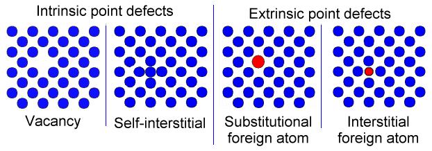

2 Types of Defects Screw line defect Edge line defect Volumetric defects 2
3 Line defects: Dislocations Elementary Line Defects u: dislocation line b: Burgers vector Screw: u b Edge: u b If you determine b and u, you have identified the dislocation Dislocation creation, motion, annihilation, and properties (electrical, optical) are function of dislocation type and line direction 3


4 Line Defects Current Issues Dislocations continue to influence critical aspects related to device performance solar cells, LEDS Multicrystalline Si solar cells Non-destructive methods for locating and identifying dislocations remain critical Dislocations as Memristors in SrTiO 3 K. Hartman et al, Appl. Phys. Lett. 93, (2008). III-V multijunction solar cells K. Szot et al, Nature Materials. 5, 312 (2006). M. Yamaguchi et al, Solar Energy 82, 173 (2008). 4
 little surface")
. Y.N. Picard et al, Appl. Phys. Lett. 91, 014101 (2007).")
5 Present Dislocation Imaging Approaches Various techniques suffer certain limitations: TEM destructive, confined area XRD not local but global SWBXT - requires a synchrotron x-ray source AFM - contact, indirectly images dislocations Chemical etching - destructive Luminescence (CL, PL, EL) little surface information, may require pre-processing, requires pre-existing knowledge of optical behavior X-TEM of AlN AFM of MBE GaN B. Heying et al, J. Appl. Phys. 85, 6470 (1999). Y.N. Picard et al, Appl. Phys. Lett. 91, (2007). Dislocation Density Average Dislocation Separation 10 8 /cm 2 1 µm 10 5 /cm 2 32 µm 5

6 Electron Channeling Contrast Imaging (ECCI) ECCI image of MOCVD GaN film Non-destructive Non-contact Commercial SEM Dislocation imaging Atomic morphology Orientation contrast 2 µm Phase identification 6
7 Electron Channeling η: backscattered electron yield η is a strong function of the relative orientation between incident electron beam and crystal Discovered by D.G. Coates, Phil. Mag. 16, 1179 (1967). David C. Joy, Dale E. Newbury, and David L. Davidson. "Electron channeling patterns in the scanning electron microscope." Journal of Applied Physics53.8 (1982): R81-R122. 7
")
 O. Engler and V.")

8 Diffraction in the SEM Electron Backscatter Diffraction (EBSD) Electron Channeling Pattern (ECP) O. Engler and V. Randle, Introduction to Texture Analysis, 2 nd. Edition, CRC Press


9 Channeling in the SEM Adapted from K. Z. Baba-Kishi, J. Mater. Sci. 37, (2002)1715. Forescatter Geometry Backscatter Geometry Low Magnification BSE Image 9
10 Electron Channeling Contrast Imaging It should in principle be possible to use the scanning electron microscope to detect dislocations by the direct examination of unetched crystal surfaces. It is only necessary to orientate the crystal at the Bragg position and the local bending of these crystallographic planes should produce the necessary contrast. Such contrast should be directional and could lead to Burgers vector determination. G.R. Booker, AMB Shaw, M.J. Whelan and P.B. Hirch, Philosophical Magazine 16, 1185 (1967). Intensity fluctuation due to local lattice bending by dislocation This is the basis for nondestructive defect imaging by ECCI J. Ahmed et al, J. Microscopy 195, 197 (1999). 10
. J. Ahmed et al, J. Microscopy 195, 197 (1999).")
11 Previous ECCI Work Si (111) - dislocations Cu - Persistent slip bands (PSBs) ECCI g 400 TEM ECCI ECCI g 220 J.T. Czernuszka et al, Phil. Mag. Lett. 62, 227 (1990). J. Ahmed et al, J. Microscopy 195, 197 (1999). 11


12 More Recent ECCI Results MOVPE GaN film on sapphire Individual dislocations can be imaged in an SEM Atomic steps visible C. Trager-Cowan et al, Phys. Rev. B. 75, (2007). 12


13 Channeling vs. Conventional SEM Backscatter Electron Detection On Diffraction Condition Secondary Electron Detection Conventional SEM GaN (0001) 13
14 Two Geometries Incident e-beam ECCI Incident e-beam Interaction volume Backscattered electrons Interaction volume Forescattered electrons 14


15 Example Experimental Approaches Forescatter Geometry Backscatter Geometry Philips XL-30 FEI Quanta 600 Courtesy of Oxford Instruments Forescatter diodes on EBSD kv, 4-6 spot size Samples tilted na s of current Annulus BSE detector kv, spot size Samples tilted
 2.")
 M. A.")


16 Modern ECCI Approach 1. BSE Image Single Crystal at Lowest Magnification GaN (0001) 2. Use Resultant ECP to Orient Sample (Tilt/Rotate) 3. Magnify to Sample Surface GaN (0001) M. A. Crimp, Scanning electron microscopy imaging of dislocations in bulk materials, using electron channeling contrast. Microsc. Res. Tech. 69, 374 (2006). R.J. Kamaladasa, Y.N. Picard, Basic principles and application of electron channeling in a scanning electron microscope for dislocation analysis Microscopy: Science, Technology, Education and Applications. Vol. 4, 1583 (2011). 16
17 ECCI Methods Important Points 1. Channeling signal is much weaker than topographic and Z-contrast information in BSE image 2. Detector-sample positioning (working distance) needs to be optimized to maximize BSE collection 3. Detector gain settings (brightness/contrast/gamma) will need adjusting to maximize channeling BSE contrast 17


![screw dislocations [0002] [0110] [2110] 20 µm](/docs-images/74/70819442/images/18-2.jpg "Vertical growth: Top Mesa > Bottom Mesa? Y.N.")
18 Single Screw Dislocation (4H-SiC) Secondary Electron Image Forescattered Electron Images {0112} facets? [2110] Atomic Step morphology centers about screw dislocations [0002] [0110] [2110] 20 µm Vertical growth: Top Mesa > Bottom Mesa? Y.N. Picard et al, Appl. Phys. Lett. 90, (2007). 18
 2 µm")


19 Single Screw Dislocation = Intensity Fluctuation Electron Channeling Contrast Imaging (ECCI) 2 µm Intensity fluctuation local lattice bending due to dislocation Forescattered electrons or FSE 2 µm 19 J. Ahmed et al, J. Microscopy 195, 197 (1999). Secondary electrons Y.N. Picard et al, Appl. Phys. Lett. 90, (2007).

20 Screw Dislocation: Contrast Burgers Vector 4H-SiC (0001) b b Y.N. Picard and M.E. Twigg, J. Appl. Phys. 104, (2008). Reversing Burgers vector, b, reverses the dark-to-light contrast D.B. Williams and C.B. Carter, from p.415 of Transmission Electron Microscopy, Plenum Press, New York (1996). 20


21 ECCI of GaN Threading dislocations = dark/light spots atomic steps = lines GaN (0001) 10 µm 2 µm Defect imaging by ECCI resolvable over areas approaching 50 x 50 μm 21

![c-axis [0001] GaN (0001) GaN](/docs-images/74/70819442/images/22-1.jpg "(0001) b b b Two distinct")


22 Screw vs. Edge Delineation by ECCI c-axis [0001] GaN (0001) GaN (0001) b b b Two distinct intensity fluctuations: Stronger and weaker Screw > Edge 500 nm b GaN a = Å Screw: c = Å b = c <0001> Edge: b = a/3 <1120> 22


23 ECCI Validation HVPE GaN Substrates ECCI pre-etching ECCI spot features SEM post-etching Defect etch pits MgO:KOH etching confirms ECCI features are dislocations Larger feature = Larger etch pit SEM post-etching (b) TEM Site-specific TEM confirms differentiation between edge and mixed dislocations (c) Edge defects Larger etch pit = Mixed dislocation Screw defect R.J. Kamaladasa et. al. Journal of Microscopy, 244(3), (2011)
 film on 4H-SiC Individual grains Threading dislocations along low-angle")

. X.J. Ning et al, J. Mater. Res. 11, 580 (1996).")
24 Edge Dislocations on Low-Angle Grain Boundaries MOVPE GaN film on sapphire ECCI MOCVD GaN (0001) film on 4H-SiC Individual grains Threading dislocations along low-angle grain boundaries C. Trager-Cowan et al, Phys. Rev. B. 75, (2007). γ = 25.1 ; s g = 0 Orientation contrast imaging A. Day and P. Trimby, Channel 5 Instruction Manual, HKL Technologies, Y.N. Picard et al, Appl. Phys. Lett. 91, (2007). X.J. Ning et al, J. Mater. Res. 11, 580 (1996). ECCI technique sensitive to threading edge dislocations 24
.")
25 Edge Dislocations on Low-Angle Grain Boundaries X.J. Ning et al, J. Mater. Res. 11, 580 (1996). ECCI technique sensitive to threading edge dislocations 25
. Y.N. Picard et. al. Scripta Mater. 61, 773 (2009).")
26 Simulating Threading Dislocation Contrast GaN (0001) Resolving dislocation type M.E. Twigg and Y.N. Picard. J. Appl. Phys. 105, (2009). Y.N. Picard et. al. Scripta Mater. 61, 773 (2009). Resolving edge dislocation directionality 26
 GaN (0001) 1 µm Y.N. Picard et.")

27 Comparing ECCI Geometries Forescatter ECCI Backscatter ECCI GaN (0001) GaN (0001) 1 µm Y.N. Picard et. al. Scripta Mater. 61, 773 (2009). Surface distortion: Screw dislocation > Edge dislocation 27

![[1010] g = [1210] 500 nm W.J. Tunstall et. al. Phil. Mag.](/docs-images/74/70819442/images/28-2.jpg "9, 99 (1964). (as taken from D.B. Williams and C.B. Carter, p.")
, 12-16 (2012).")
28 Contrast Dependent on Diffraction Vector GaN (0001): Rotating diffraction vector, g, rotates dark-light contrast features g = [1010] g = [1210] 500 nm W.J. Tunstall et. al. Phil. Mag. 9, 99 (1964). (as taken from D.B. Williams and C.B. Carter, p.415 of Transmission Electron Microscopy, Y.N. Picard et. al. Microscopy Today. 20 (2), (2012). Plenum Press, New York (1996).) 28
 1 µm Surface Penetrating Vertical Dislocation Y.N. Picard et al, J. Appl. Phys. 104, (2008) 124906.")
29 Dislocation Channeling Contrast Line Direction ECCI of Screw Dislocation in 4H-SiC (0001) Dark-Light Spot Feature J. Ahmed et al, J. Microscopy 195, 197 (1999). ECCI of Edge Dislocation in SrTiO 3 (100) 1 µm Surface Penetrating Vertical Dislocation Y.N. Picard et al, J. Appl. Phys. 104, (2008) Dark-Light Line Feature 500 nm Sub-Surface Horizontal Dislocation 29
30 Dislocation Line Direction Insights from Etching SrTiO 3 (100): HF acid etching is defect selective ECCI SEM post-etching ECCI SEM post-etching Line feature is sub-surface, no etch feature Half-loop configuration 2 µm 2 µm R.J. Kamaladasa and Y.N. Picard,, Journal of Electronic Materials, 40(11), (2011) HF etching: W. Jiang, CMU 1:1 Correlation for surface penetrating dislocations 30
 g b x u = 0 (edge) Invisibility criteria Dislocation")

 Result: b identification (dislocation")
31 ECCI Invisibility Criteria g = 100 g = 110 SrTiO 3 (001) g b = 0 (screw) g b x u = 0 (edge) Invisibility criteria Dislocation line: u = <100> Burgers vector: b Diffraction vector: g g = 010 Independent variable g vector Dependent variable Dislocation feature contrast (strong, weak, invisible) Feature shape u (dislocation line) Result: b identification (dislocation determination) 31
 GaN (0001) g = 100 g =")

 g = 010 2 µm")

32 ECCI Various Dislocation Interactions SrTiO 3 (001) GaN (0001) g = 100 g = Y.N. Picard et. al. Microscopy Today. 20 (2), (2012). SrTiO 3 (001) g = µm Surface-penetrating half-loops g = 010 Sub-surface dislocation loops Y.N. Picard et. al. Microscopy Today. 20 (2), (2012). 5 µm 32


33 Dislocations along slip line Each dislocation increases slip line height by a unit of the Burgers vector magnitude W. Jiang, R.J. Kamaladasa, Y. Lu, R. Berechman, P.A. Salvador, J.A. Bain, Y.N. Picard, M. Skowronski, Local heating-induced plastic deformation in resistive switching devices Journal of Applied Physics, 110(5), (2011). 33
 Y.N.")


34 Accurate Simulation of ECCI features GaSb (001) Y.N. Picard, et. al., Future prospects for defect and strain analysis in the SEM via electron channeling Microscopy Today. 20 (2), (2012). 34
![Accurate Simulation of ECCI features SrTiO 3 (001) Perovskite singlecrystal (001) b u = [011] b Screw dislocations inclined 45 degrees to (001) surface Y.N. Picard, M.](/docs-images/74/70819442/images/35-0.jpg "Liu, J. Lammatao, R.J. Kamaladasa, and M.")
35 Accurate Simulation of ECCI features SrTiO 3 (001) Perovskite singlecrystal (001) b u = [011] b Screw dislocations inclined 45 degrees to (001) surface Y.N. Picard, M. Liu, J. Lammatao, R.J. Kamaladasa, and M. De Graef, Theory of Dynamical Electron Channeling Contrast Images of Near-Surface Crystal Defects Ultramicroscopy, 146, (2014). 35
GaN substrate ECCI image of")
GaN substrate No")

36 Non-destructive Mapping Pre/Post Growth Wet etched surface of GaN homoepitaxy after growth n-gan (0001)GaN substrate ECCI image of the (0001)GaN substrate before growth Screw TD Edge TD Cross sectional TEM images of 10nm GaN grown on (0001)GaN substrate No new dislocations All dislocations from the substrate propagate to homoepitaxial film F. Liu, et. al., Journal of Crystal Growth, 387, (2014). 36

GaN substrate Density (10 6 cm -2 ) Average σ")
 GaN substrate before growth F.")
. TD 5.")
37 ECCI of In 0.1 Ga 0.9 N/GaN Multi-Quantum Wells Screw TD In 0.1 Ga 0.9 N/GaN MQW Topographic mode Edge TD TD n-gan (0001)GaN substrate Density (10 6 cm -2 ) Average σ V-defects V-defect ECCI image of (0001) GaN substrate before growth F. Liu, et. al., Journal of Crystal Growth, 387, (2014). TD One-to-One Correlation SEM image of as grown surface of In 0.1 Ga 0.9 N/GaN MQW (nonchanneling condition) 37


38 ECCI of GaP on Si (100) S.D. Carnevale, J. Deitz, J. Carlin, Y.N. Picard, D.W. McComb, M. De Graef, S. Ringel, T.J. Grasssman, Applications of Electron Channeling Contrast Imaging for the Rapid Characterization of Extended Defects in III-V/Si Heterostructures IEEE Journal of Photovoltaics, 5(2) (2015). Threading Dislocations Misfit Dislocations Stacking Fault S. D. Carnevale, J. I. Deitz, T. J. Grassman, J. A. Carlin, Y.N. Picard, M. De Graef, S. A. Ringel, Rapid Misfit Dislocation Characterization in Heteroepitaxial III-V/Si Thin Films by Electron Channeling Contrast Imaging Applied Physics Letters, 104, (2014). 38

. M. Yan et. al., Appl. Phys.")
39 Anti-Phase Domain Boundaries c-afm of La 0.7 Sr 0.3 MnO 3 ECCI of La 0.7 Sr 0.3 MnO 3 L. Balcells et. al., Phys. Rev. B. 92, (2015). M. Yan et. al., Appl. Phys. Lett. 107, (2015). 39


40 Si-Ge Misfit Dislocations g = g = 2-20 SiGe (001) film on Si: High density of misfit dislocations on {110} g =
41 Point Defect Clustering at Dislocations Screw dislocations from substrate nucleate hillocks Hillock apex corresponds to drop in ev NBE intensity 41

42 ECCI correlation to Optoelectronic Behavior 42

 slip bands have high stress")
43 ECCI of Slip Bands in Steel 30 wt% Mn Steel under high strain rate hardening behavior Tensile axis is out-of-plane a,b) planar dislocation glide {111} to slip band formation; c) slip bands have high stress between them 43


44 ECCI of Slip Bands and Dislocations Evolution in Steel 44

45 Sub-grain boundary characterization 45

46 Inverted ECCI High Resolution Bright-Field 46

 and high density")
47 ECCI of a High Entropy Alloy Planar slip in a CoCrFeMnNi alloy Dislocations progress to dislocation cells (DC) and high density dislocation walls (HDDW) 47
48 Summary Defect imaging via SEM highly accessible via electron channeling FEG SEM + BSE Detector Must consider crystallography g vector and defect geometry Opportunities for progress Improved BSE detector sensitivity Coordination with in situ methods inside the SEM Coordination with SPM and other SEM modes defect-property correlations Automated high-speed imaging and mapping of millimeter areas Reliable defect identification accurate simulations Reliable g vector control informed by EBSD and/or SACP I recommend this review article: 48

49 Become a ECAMT-FIG Member Join us at our next ECAMT-FIG Business Meeting Tuesday, July 26 12:15-1:15 pm Room C223 Organizers: Jorg Wiezorek, University of Pittsburgh Yoosuf Picard, Carnegie Mellon University Robert Stroud, NanoMegas Sergei Roviumov, University of Notre Dame A Pre-Meeting Congress hosted by the MSA Electron Crystallography and Automated Mapping Techniques -- Focused Interest Group Exploiting the Diffractive Properties of Electrons for Solving Materials Problems
50 Become a ECAMT-FIG Member Join us at our next ECAMT-FIG Business Meeting Tuesday, July 26 12:15-1:15 pm Room C223 Today s slides will be posted for ECAMT-FIG members [ FUTURE ACTIVITIES / NEW RESOURCES ] The Electron Crystallography & Automated Mapping Techniques Focused Interest Group (ECAMT-FIG) is a community of MSA members with a common interest in crystallography and advanced electron methods for materials characterization. Our goal is to provide a platform for the distribution and discussion of ECAMT-relevant information chosen by the membership. Our activities include the hosting of pre-meeting congresses and symposia during the annual M&M meeting. We also host a luncheon and business meeting during the annual M&M meeting. ypicard@cmu.edu ECAMT-FIG Leader-Elect
Electron Channeling Contrast Imaging: Rapid Characterization of Semiconductors. Julia I. Deitz 1
 Electron Channeling Contrast Imaging: Rapid Characterization of Semiconductors Julia I. Deitz 1 Introduction For semiconductor technologies, achievement of their ultimate potential depends greatly upon
Application of Scanning Electron Microscope to Dislocation Imaging in Steel
 Application of Scanning Electron Microscope to Dislocation Imaging in Steel Masaaki Sugiyama and Masateru Shibata Advanced Technology Research Laboratories, Nippon Steel Corporation SM Business Unit, JEOL
Electron channelling contrast imaging (ECCI) an amazing tool for observations of crystal lattice defects in bulk samples
 an amazing tool for observations of crystal lattice defects in bulk samples") Electron channelling contrast imaging (ECCI) an amazing tool for observations of crystal lattice defects in bulk samples Stefan Zaefferer with contributions of N. Elhami, (general & steels) Z. Li F. Ram,
Electron channelling contrast imaging (ECCI) an amazing tool for observations of crystal lattice defects in bulk samples Stefan Zaefferer with contributions of N. Elhami, (general & steels) Z. Li F. Ram,
ECCI of AlGaN/GaN HEMT structures grown on Si
 ECCI of AlGaN/GaN HEMT structures grown on Si D. Thomson 1, G. Naresh-Kumar 1, B. Hourahine 1, C. Trager-Cowan 1, P. Wright 2 and T. Martin 2 1 Dept. Of Physics, SUPA, University of Strathclyde, Glasgow
TEM Study of the Morphology Of GaN/SiC (0001) Grown at Various Temperatures by MBE
 Grown at Various Temperatures by MBE") TEM Study of the Morphology Of GaN/SiC (0001) Grown at Various Temperatures by MBE W.L. Sarney 1, L. Salamanca-Riba 1, V. Ramachandran 2, R.M Feenstra 2, D.W. Greve 3 1 Dept. of Materials & Nuclear Engineering,
TEM Study of the Morphology Of GaN/SiC (0001) Grown at Various Temperatures by MBE W.L. Sarney 1, L. Salamanca-Riba 1, V. Ramachandran 2, R.M Feenstra 2, D.W. Greve 3 1 Dept. of Materials & Nuclear Engineering,
TEM and Electron Diffraction Keith Leonard, PhD (1999) U. Cincinnati
 U. Cincinnati") TEM and Electron Diffraction Keith Leonard, PhD (1999) U. Cincinnati Electron Microscopes: Electron microscopes, such as the scanning electron microscope (SEM) and transmission electron microscope (TEM)
TEM and Electron Diffraction Keith Leonard, PhD (1999) U. Cincinnati Electron Microscopes: Electron microscopes, such as the scanning electron microscope (SEM) and transmission electron microscope (TEM)
Kinematical theory of contrast
 Kinematical theory of contrast Image interpretation in the EM the known distribution of the direct and/or diffracted beam on the lower surface of the crystal The image on the screen of an EM = the enlarged
Experimental problem uniquely solved by TEM: Observation of dislocations and their dynamics. Milan Kornjaca, Physics 590B
 Experimental problem uniquely solved by TEM: Observation of dislocations and their dynamics Milan Kornjaca, Physics 590B 3000-year-old problem Why can metals be workhardened and annealed? Why is steel
Imaging with Diffraction Contrast
 Imaging with Diffraction Contrast Duncan Alexander EPFL-CIME 1 Introduction When you study crystalline samples TEM image contrast is dominated by diffraction contrast. An objective aperture to select either
Practical 2P8 Transmission Electron Microscopy
 Practical 2P8 Transmission Electron Microscopy Originators: Dr. M. L. Jenkins and Prof. J. M. Titchmarsh What you should learn from this practical Science This practical ties-in with the lecture course
Synchrotron X-Ray Topography Measurements on 4H-SiC Epitaxial Layer
 Synchrotron X-Ray Topography Measurements on 4H-SiC Epitaxial Layer Isaho KAMATA, Central Research Institute of Electric Power Industry (CRIEPI) Kamata@criepi.denken.or.jp Silicon carbide has excellent
Thin Film Scattering: Epitaxial Layers
 Thin Film Scattering: Epitaxial Layers 6th Annual SSRL Workshop on Synchrotron X-ray Scattering Techniques in Materials and Environmental Sciences: Theory and Application May 29-31, 2012 Thin films. Epitaxial
Defect and chemical analysis in the TEM
 THE UNIVERSITY Defect and chemical analysis in the TEM Defect and chemical analysis in the TEM I.P. Jones. Chemical analysis: EDX. Chemical analysis: PEELS Centre for Electron Microscopy OF BIRMINGHAM
TEM imaging and diffraction examples
 TEM imaging and diffraction examples Duncan Alexander EPFL-CIME 1 Diffraction examples Kikuchi diffraction Epitaxial relationships Polycrystalline samples Amorphous materials Contents Convergent beam electron
CHEM-E5225 :Electron Microscopy Imaging II
 CHEM-E5225 :Electron Microscopy Imaging II D.B. Williams, C.B. Carter, Transmission Electron Microscopy: A Textbook for Materials Science, Springer Science & Business Media, 2009. Z. Luo, A Practical Guide
Practical 2P8 Transmission Electron Microscopy
 Practical 2P8 Transmission Electron Microscopy Originators: Dr. N.P. Young and Prof. J. M. Titchmarsh What you should learn from this practical Science This practical ties-in with the lecture course on
EBSD Electron BackScatter Diffraction Principle and Applications
 EBSD Electron BackScatter Diffraction Principle and Applications Dr. Emmanuelle Boehm-Courjault EPFL STI IMX Laboratoire de Simulation des Matériaux LSMX emmanuelle.boehm@epfl.ch 1 Outline! Introduction!
EBSD Basics EBSD. Marco Cantoni 021/ Centre Interdisciplinaire de Microscopie Electronique CIME. Phosphor Screen. Pole piece.
 EBSD Marco Cantoni 021/693.48.16 Centre Interdisciplinaire de Microscopie Electronique CIME EBSD Basics Quantitative, general microstructural characterization in the SEM Orientation measurements, phase
Carnegie Mellon MRSEC
 Carnegie Mellon MRSEC Texture, Microstructure & Anisotropy, Fall 2009 A.D. Rollett, P. Kalu 1 ELECTRONS SEM-based TEM-based Koseel ECP EBSD SADP Kikuchi Different types of microtexture techniques for obtaining
Structural Analysis in Low-V-defect Blue and Green GaInN/GaN Light Emitting Diodes
 Mater. Res. Soc. Symp. Proc. Vol. 1040 2008 Materials Research Society 1040-Q03-02 Structural Analysis in Low-V-defect Blue and Green GaInN/GaN Light Emitting Diodes Mingwei Zhu 1,2, Theeradetch Detchprohm
Recent progress in the growth of heteroepitaxial diamond for detector applications
 Recent progress in the growth of heteroepitaxial diamond for detector applications 4th ADAMAS Workshop at GSI 2015-12-03 2015-12-04 Michael Mayr, Oliver Klein, Martin Fischer, Stefan Gsell, Matthias Schreck
TEM imaging and diffraction examples
 TEM imaging and diffraction examples Duncan Alexander EPFL-CIME 1 Diffraction examples Kikuchi diffraction Epitaxial relationships Polycrystalline samples Amorphous materials Contents Convergent beam electron
SECTION A. NATURAL SCIENCES TRIPOS Part IA. Friday 4 June to 4.30 MATERIALS AND MINERAL SCIENCES
 NATURAL SCIENCES TRIPOS Part IA Friday 4 June 1999 1.30 to 4.30 MATERIALS AND MINERAL SCIENCES Answer five questions; two from each of sections A and B and one from section C. Begin each answer at the
3. Anisotropic blurring by dislocations
 Dynamical Simulation of EBSD Patterns of Imperfect Crystals 1 G. Nolze 1, A. Winkelmann 2 1 Federal Institute for Materials Research and Testing (BAM), Berlin, Germany 2 Max-Planck- Institute of Microstructure
Observation in the GB (Gentle Beam) Capabilities
 Capabilities") A field-emission cathode in the electron gun of a scanning electron microscope provides narrower probing beams at low as well as high electron energy, resulting in both improved spatial resolution and
A field-emission cathode in the electron gun of a scanning electron microscope provides narrower probing beams at low as well as high electron energy, resulting in both improved spatial resolution and
X-RAY DIFFRACTION IN SEMICONDUCTOR INDUSTRY AND RESEARCH
 X-RAY DIFFRACTION IN SEMICONDUCTOR INDUSTRY AND RESEARCH M. Leszczyński High Pressure Research Center UNIPRESS, Sokolowska 29/37, 01 142 Warsaw, Poland, e-mail: mike@unipress.waw.pl ABSTRACT The paper
Supplementary Figure 1. Three-dimensional morphology of twins in magnesium alloys. The morphology of deformation twins is usually examined using
 Supplementary Figure 1. Three-dimensional morphology of twins in magnesium alloys. The morphology of deformation twins is usually examined using two-dimensional microscopy such as optical microscope and
Microstructural Characterization of Materials
 Microstructural Characterization of Materials 2nd Edition DAVID BRANDON AND WAYNE D. KAPLAN Technion, Israel Institute of Technology, Israel John Wiley & Sons, Ltd Contents Preface to the Second Edition
Relation between Microstructure and 2DEG Properties of AlGaN/GaN Structures
 2. Experimental The AlGaN/GaN structures have been grown by low-pressure metalorganic vapor phase epitaxy (LP-MOVPE) on c-plane sapphire substrates [2], using ammonia, TMGa and TMAl as precursors. After
Introduction to Electron Backscattered Diffraction. TEQIP Workshop HREXRD Feb 1 st to Feb 5 th 2016
 Introduction to Electron Backscattered Diffraction 1 TEQIP Workshop HREXRD Feb 1 st to Feb 5 th 2016 SE vs BSE 2 Ranges and interaction volumes 3 (1-2 m) http://www4.nau.edu/microanalysis/microprobe/interact-effects.html
In-situ Electron Microscopy Mechanical Testing for Steels
 Technical Report UDC 621. 385. 2 : 620. 17 : 669. 14 In-situ Electron Microscopy Mechanical Testing for Steels Shunsuke TANIGUCHI* Gerhard DEHM Abstract This paper outlines the techniques of in-situ electron
DEFECTS IN SILICON-GERMANIUM STRAINED EPITAXIAL LAYERS MARK DYNNA. A Thesis. Submitted to the School of Graduate Studies.
 DEFECTS IN SILICON-GERMANIUM STRAINED EPITAXIAL LAYERS By MARK DYNNA A Thesis Submitted to the School of Graduate Studies in Partial Fulfillment of the Requirements for the Degree Doctor of Philosophy
Temperature dependence of molecular beam epitaxy of GaN on SiC (0001)
") Temperature dependence of molecular beam epitaxy of GaN on SiC (0001) V. Ramachandran a, A. R. Smith a, R. M. Feenstra a and D. W. Greve b a Department of Physics, b Department of Electrical and Computer
Temperature dependence of molecular beam epitaxy of GaN on SiC (0001) V. Ramachandran a, A. R. Smith a, R. M. Feenstra a and D. W. Greve b a Department of Physics, b Department of Electrical and Computer
Optimized structural properties of wurtzite GaN on SiC(0001) grown by molecular beam epitaxy
 grown by molecular beam epitaxy") Optimized structural properties of wurtzite GaN on SiC(0001) grown by molecular beam epitaxy V. Ramachandran and R. M. Feenstra Department of Physics, Carnegie Mellon University, Pittsburgh, PA 15213 W.
Optimized structural properties of wurtzite GaN on SiC(0001) grown by molecular beam epitaxy V. Ramachandran and R. M. Feenstra Department of Physics, Carnegie Mellon University, Pittsburgh, PA 15213 W.
Detrimental effects of dislocations II
 Detrimental effects of dislocations II Band diagram around a charged dislocation e - - - - - - - - Charged dislocation line Electrons get scattered by charged dislocations Mobility vs. sheet charge in
Introduction to Engineering Materials ENGR2000 Chapter 4: Imperfections in Solids. Dr. Coates
 Introduction to Engineering Materials ENGR000 Chapter 4: Imperfections in Solids Dr. Coates Learning Objectives 1. Describe both vacancy and self interstitial defects. Calculate the equilibrium number
Dislocations Linear Defects
 Dislocations Linear Defects Dislocations are abrupt changes in the regular ordering of atoms, along a line (dislocation line) in the solid. They occur in high density and are very important in mechanical
Lecture # 11 References:
 Lecture # 11 - Line defects (1-D) / Dislocations - Planer defects (2D) - Volume Defects - Burgers vector - Slip - Slip Systems in FCC crystals - Slip systems in HCP - Slip systems in BCC Dr.Haydar Al-Ethari
In-situ TEM straining of tetragonal martensite of Ni-Mn-Ga alloy
 , 04007 (2009) DOI:10.1051/esomat/200904007 Owned by the authors, published by EDP Sciences, 2009 In-situ TEM straining of tetragonal martensite of Ni-Mn-Ga alloy Yanling Ge a 1, 1, Ilkka Aaltio a a, Simo-Pekka
Growth and characterization of tensile strained Ge on Ge 1-x Sn x buffers for novel channel layers
 The 5th International Symposium on Advanced Science and Technology of Silicon Materials (JSPS Si Symposium), Nov. 10-14, 2008, Kona, Hawaii, USA Growth and characterization of tensile strained Ge on Ge
Transmission Kikuchi Diffraction in the Scanning Electron Microscope
 Transmission Kikuchi Diffraction in the Scanning Electron Microscope Robert Keller, Roy Geiss, Katherine Rice National Institute of Standards and Technology Nanoscale Reliability Group Boulder, Colorado
Electron microscopy II
 Electron microscopy II Nanomaterials characterization I RNDr. Věra Vodičková, PhD. Interaction ction: electrons solid matter Signal types SE.secondary e - AE Auger s e - BSE back scattered e - X-ray photons,
Supplementary Figure 1: Geometry of the in situ tensile substrate. The dotted rectangle indicates the location where the TEM sample was placed.
 Supplementary Figures Supplementary Figure 1: Geometry of the in situ tensile substrate. The dotted rectangle indicates the location where the TEM sample was placed. Supplementary Figure 2: The original
STUDY & ANALYSIS OF ALUMINIUM FOIL AND ANATASE TITANIUM OXIDE (TiO2) USING TRANSMISSION ELECTRON MICROSCOPY
 USING TRANSMISSION ELECTRON MICROSCOPY") STUDY & ANALYSIS OF ALUMINIUM FOIL AND ANATASE TITANIUM OXIDE (TiO2) USING TRANSMISSION ELECTRON MICROSCOPY Ayush Garg Department of Chemical and Materials Engineering, University of Auckland, Auckland,
STUDY & ANALYSIS OF ALUMINIUM FOIL AND ANATASE TITANIUM OXIDE (TiO2) USING TRANSMISSION ELECTRON MICROSCOPY Ayush Garg Department of Chemical and Materials Engineering, University of Auckland, Auckland,
Crystallographic Distribution of Low Angle Grain Boundary Planes in Magnesium Oxide
 Citation & Copyright (to be inserted by the publisher ) Crystallographic Distribution of Low Angle Grain Boundary Planes in Magnesium Oxide D.M. Saylor 1, A. Morawiec 2, K.W. Cherry 1, F.H. Rogan 1, G.S.
Supplementary Materials for
 advances.sciencemag.org/cgi/content/full/4/8/eaat4712/dc1 Supplementary Materials for In situ manipulation and switching of dislocations in bilayer graphene Peter Schweizer, Christian Dolle, Erdmann Spiecker*
Deformation Microstructure and Texture in a Cold-Rolled Austenitic Steel with Low Stacking-Fault Energy
 Materials Transactions, Vol. 51, No. 4 (2010) pp. 620 to 624 Special Issue on Crystallographic Orientation Distribution and Related Properties in Advanced Materials II #2010 The Japan Institute of Metals
Electron channelling contrast observations in deformed Mg alloys prepared with ion milling
 IOP Conference Series: Materials Science and Engineering OPEN ACCESS Electron channelling contrast observations in deformed Mg alloys prepared with ion milling To cite this article: S Kaboli et al 2014
Supplementary information. Homogeneity and variation of donor doping in
 Supplementary information to Homogeneity and variation of donor doping in Verneuil-grown SrTiO3:Nb single crystals C. Rodenbücher, M. Luysberg, A. Schwedt, V. Havel, F. Gunkel, J. Mayer, and R. Waser I.
Vertical nano-composite heteroepitaxial thin films with manganites and ferroelectrics. Yonghang Pei Physics Department
 Vertical nano-composite heteroepitaxial thin films with manganites and ferroelectrics Yonghang Pei Physics Department Outline Introduction to MultiFerroics La 1 x Sr x MnO 3 Experiment Summary and Future
Conventional TEM. N o r t h w e s t e r n U n i v e r s i t y - M a t e r i a l s S c i e n c e
 Conventional TEM STEM N o r t h w e s t e r n U n i v e r s i t y - M a t e r i a l s S c i e n c e Reciprocity 1 1 C CCCCCCCC(2ππππππ. rr) CCCCCC(2ππππππ. rr) Reciprocity 2 1 C+D CC(gg)CCCCCC(2ππππππ.
Faceted inversion domain boundary in GaN films doped with Mg
 Faceted inversion domain boundary in GaN films doped with Mg L. T. Romano* and J.E. Northrup Xerox Palo Alto Research Center, 3333 Coyote Hill Road, Palo Alto, CA 94304 A. J. Ptak and T.H. Myers Department
factured pillars, even though the strength is significantly higher than in the bulk. These yield stress values, y
 Abstract The size effect in body-centered cubic (bcc) metals was comprehensively investigated through microcompression tests performed on focused ion beam machined tungsten (W), molybdenum (Mo) and niobium
EPITAXY extended single-crystal film formation on top of a crystalline substrate. Homoepitaxy (Si on Si) Heteroepitaxy (AlAs on GaAs)
 Heteroepitaxy (AlAs on GaAs)") extended single-crystal film formation on top of a crystalline substrate Homoepitaxy (Si on Si) Heteroepitaxy (AlAs on GaAs) optoelectronic devices (GaInN) high-frequency wireless communication devices
extended single-crystal film formation on top of a crystalline substrate Homoepitaxy (Si on Si) Heteroepitaxy (AlAs on GaAs) optoelectronic devices (GaInN) high-frequency wireless communication devices
Dislocation contrast in electron channelling contrast images as projections of strain-like components
 Available online at www.sciencedirect.com ScienceDirect Materials Today: Proceedings 5 (2018) 14652 14661 www.materialstoday.com/proceedings EDS 2016 Dislocation contrast in electron channelling contrast
E45 Midterm 01 Fall 2007! By the 0.2% offset method (shown on plot), YS = 500 MPa
, YS = 500 MPa") 1.!Mechanical Properties (20 points) Refer to the following stress-strain plot derived from a standard uniaxial tensile test of a high performance titanium alloy to answer the following questions. Show
1.!Mechanical Properties (20 points) Refer to the following stress-strain plot derived from a standard uniaxial tensile test of a high performance titanium alloy to answer the following questions. Show
3. Solidification & Crystalline Imperfections
 3. Solidification & Crystalline Imperfections solidification (casting process) of metals divided into two steps (1) nucleation formation of stable nuclei in the melt (2) growth of nuclei into crystals
On-axis Transmission Kikuchi Diffraction in the SEM. Performances and Applications
 On-axis Transmission Kikuchi Diffraction in the SEM. Performances and Applications Etienne Brodu, Emmanuel Bouzy, Jean-Jacques Fundenberger Séminaire «les microscopies électroniques à Metz et à Nancy»
TEM Study of Bulk AlN Growth by Physical Vapor Transport
 TEM Study of Bulk AlN Growth y Physical Vapor Transport W.L. Sarney 1, L. Salamanca-Ria 1, T. Hossain 2, P. Zhou 2, H.N. Jayatirtha 2, H.H. Kang 1, R.D. Vispute 1, M. Spencer 2, K.A. Jones 3 1 Dept. of
Sr and Pb additions. L. Affleck, C. Leach *
 Microstructures of BaTiO 3 based PTC thermistors with Ca, Sr and Pb additions Abstract L. Affleck, C. Leach * Manchester Materials Science Centre University of Manchester and UMIST Grosvenor Street, Manchester
Structural Properties of GaN Films Grown by Molecular Beam Epitaxy on Singular and Vicinal 6H-SiC(0001)
") Structural Properties of GaN Films Grown by Molecular Beam Epitaxy on Singular and Vicinal 6H-SiC(0001) C. D. Lee, 1 R. M. Feenstra, 1 O. Shigiltchoff, 2 R. P. Devaty 2 and W. J. Choyke 2 1 Department
Structural Properties of GaN Films Grown by Molecular Beam Epitaxy on Singular and Vicinal 6H-SiC(0001) C. D. Lee, 1 R. M. Feenstra, 1 O. Shigiltchoff, 2 R. P. Devaty 2 and W. J. Choyke 2 1 Department
Advances in EBSD Analysis Using Novel Dynamical Pattern Simulation Software
 Advances in EBSD Analysis Using Novel Dynamical Pattern Simulation Software Bruker Nano GmbH, Berlin Webinar, November 5 th, 2014 Innovation with Integrity Presenters Dr. Daniel Goran Product Manager EBSD,
Thin Film Scattering: Epitaxial Layers
 Thin Film Scattering: Epitaxial Layers Arturas Vailionis First Annual SSRL Workshop on Synchrotron X-ray Scattering Techniques in Materials and Environmental Sciences: Theory and Application Tuesday, May
Electrochemical Oxidation, Threading Dislocations and the Reliability of GaN HEMTs
 Electrochemical Oxidation, Threading Dislocations and the Reliability of GaN HEMTs Carl V. Thompson 1,3 Dept. of Materials Science and Engineering, M.I.T. Primary collaborators: Wardhana A. Sasangka 1,
Final Report for AOARD Grant FA Development of direct band gap group-iv. March, 2012
 Final Report for AOARD Grant FA2386-11-1-4037 Development of direct band gap group-iv semiconductor with the incorporation of Sn March, 2012 Name of Principal Investigators: Prof. H. H. Cheng - e-mail
Microstructure of Friction Stir Welded 6061 Aluminum Alloy
 Proceedings of the 9 th International Conference on Aluminium Alloys (2004) Edited by J.F. Nie, A.J. Morton and B.C. Muddle Institute of Materials Engineering Australasia Ltd 878 Microstructure of Friction
Deformation Twinning in Bulk Aluminum with Coarse Grains
 Proceedings of the 12th International Conference on Aluminium Proceedings Alloys, of the September 12th International 5-9, 2010, Yokohama, Conference Japan on 2010 Aluminum The Japan Alloys, Institute
Twins & Dislocations in HCP Textbook & Paper Reviews. Cindy Smith
 Twins & Dislocations in HCP Textbook & Paper Reviews Cindy Smith Motivation Review: Outline Crystal lattices (fcc, bcc, hcp) Fcc vs. hcp stacking sequences Cubic {hkl} naming Hcp {hkil} naming Twinning
LBIC investigations of the lifetime degradation by extended defects in multicrystalline solar silicon
 LBIC investigations of the lifetime degradation by extended defects in multicrystalline solar silicon Markus Rinio 1, Hans Joachim Möller 1 and Martina Werner 2, 1 Institute for Experimental Physics, TU
Application of Advanced Techniques for Metals Identification and Characterisation
 Application of Advanced Techniques for Metals Identification and Characterisation David N Githinji Department of Manufacturing, Industrial & Textile Engineering, Moi University, P.O Box 3900-30100, Eldoret,
High-resolution electron microscopy of grain boundary structures in yttria-stabilized cubic zirconia
 Mat. Res. Soc. Symp. Proc. Vol. 654 2001 Materials Research Society High-resolution electron microscopy of grain boundary structures in yttria-stabilized cubic zirconia K. L. Merkle, L. J. Thompson, G.-R.
Crystallographic Textures Measurement
 Crystallographic Textures Measurement D. V. Subramanya Sarma Department of Metallurgical and Materials Engineering Indian Institute of Technology Madras E-mail: vsarma@iitm.ac.in Macrotexture through pole
Movement of edge and screw dislocations
 Movement of edge and screw dislocations Formation of a step on the surface of a crystal by motion of (a) n edge dislocation: the dislocation line moves in the direction of the applied shear stress τ. (b)
The Effect of Crystallographic Texture on the Wrap Bendability in AA5754-O Temper Sheet Alloy
 Proceedings of the 12th International Conference on Aluminium Alloys, September 5-9, 2010, Yokohama, Japan 2010 The Japan Institute of Light Metals pp. 607-612 607 The Effect of Crystallographic Texture
3.46 OPTICAL AND OPTOELECTRONIC MATERIALS
 Badgap Engineering: Precise Control of Emission Wavelength Wavelength Division Multiplexing Fiber Transmission Window Optical Amplification Spectrum Design and Fabrication of emitters and detectors Composition
III III a IIOI OlD IIO OlD 110 II II III lulu II OI IIi
 (19) United States III III a IIOI OlD IIO 1101 100 1101 OlD 110 II II III lulu II OI IIi US 20060270076A1 (12) Patent Application Publication (10) Pub. No.: US 2006/0270076 Al Imer et al. (43) Pub. Date:
A Quantitative Evaluation of Microstructure by Electron Back-Scattered Diffraction Pattern Quality Variations
 Microsc. Microanal. 19, S5, 83 88, 2013 doi:10.1017/s1431927613012397 A Quantitative Evaluation of Microstructure by Electron Back-Scattered Diffraction Pattern Quality Variations SukHoonKang, 1 Hyung-Ha
Lecture # 11. Line defects (1D) / Dislocations
 / Dislocations") Lecture # 11 - Line defects (1-D) / Dislocations - Planer defects (2D) - Volume Defects - Burgers vector - Slip - Slip Systems in FCC crystals - Slip systems in HCP - Slip systems in BCC References: 1-
Lecture # 11 - Line defects (1-D) / Dislocations - Planer defects (2D) - Volume Defects - Burgers vector - Slip - Slip Systems in FCC crystals - Slip systems in HCP - Slip systems in BCC References: 1-
Anomaly of Film Porosity Dependence on Deposition Rate
 Anomaly of Film Porosity Dependence on Deposition Rate Stephen P. Stagon and Hanchen Huang* Department of Mechanical Engineering, University of Connecticut, Storrs, CT 06269 J. Kevin Baldwin and Amit Misra
A Combined Discrete-dislocation/Scaledependent Crystal Plasticity Analysis of Deformation and Fracture in Nanomaterials. Presented by: Derek Columbus
 MS Thesis Defense A Combined Discrete-dislocation/Scaledependent Crystal Plasticity Analysis of Deformation and Fracture in Nanomaterials Presented by: Derek Columbus Advisor: Dr. Mica Grujicic Department
12/10/09. Chapter 4: Imperfections in Solids. Imperfections in Solids. Polycrystalline Materials ISSUES TO ADDRESS...
 Chapter 4: ISSUES TO ADDRESS... What are the solidification mechanisms? What types of defects arise in solids? Can the number and type of defects be varied and controlled? How do defects affect material
Introduction to Nitride Semiconductor Blue Lasers and Light Emitting Diodes
 Introduction to Nitride Semiconductor Blue Lasers and Light Emitting Diodes Edited by Shuji Nakamura and Shigefusa F. Chichibu London and New York Contents 1. Basics Physics and Materials Technology of
INTERPRETATION OF TRANSMISSION ELECTRON MICROGRAPHS
 3 INTERPRETATION OF TRANSMISSION ELECTRON MICROGRAPHS Already published in this series 1. The Operation and Calibration of the Electron Microscope 2. Electron Diffraction in the Electron Microscope In
Heterostructures of Oxides and Semiconductors - Growth and Structural Studies
 Heterostructures of Oxides and Semiconductors - Growth and Structural Studies Beamline 17B1 W20 X-ray Scattering beamline Authors M. Hong and J. R. Kwo National Tsing Hua University, Hsinchu, Taiwan H.
Precision Without Compromise
 D1 EVOLUTION Precision Without Compromise Versatile and user-friendly high resolution and multipurpose X-ray diffractometer for the characterization of advanced materials www.jvsemi.com D1 Overview Introduction
Chapter 4: Imperfections (Defects) in Solids
 in Solids") Chapter 4: Imperfections (Defects) in Solids ISSUES TO ADDRESS... What types of defects exist in solids? How do defects affect material properties? Can the number and type of defects be varied and controlled?
Chapter 4: Imperfections (Defects) in Solids ISSUES TO ADDRESS... What types of defects exist in solids? How do defects affect material properties? Can the number and type of defects be varied and controlled?
IMPERFECTIONSFOR BENEFIT. Sub-topics. Point defects Linear defects dislocations Plastic deformation through dislocations motion Surface
 IMPERFECTIONSFOR BENEFIT Sub-topics 1 Point defects Linear defects dislocations Plastic deformation through dislocations motion Surface IDEAL STRENGTH Ideally, the strength of a material is the force necessary
NEMI Sn Whisker Modeling Group Part 2:Future Work
 NEMI Sn Whisker Modeling Group Part 2:Future Work IPC/NEMI Meeting Maureen Williams, NIST Irina Boguslavsky, NEMI Consultant November 7, 2002 New Orleans, LA Capabilities of NEMI Modeling Group NEMI Fundamental
TRANSMISSION ELECTRON MICROSCOPY OF OPTOELECTRONIC MATERIALS BASICS AND ADVANCED TECHNIQUES
 TRANSMISSION ELECTRON MICROSCOPY OF OPTOELECTRONIC MATERIALS BASICS AND ADVANCED TECHNIQUES Fritz Phillipp Max-Planck-Institut für Metallforschung, Heisenbergstr. 3, D-70569 Stuttgart, Germany ABSTRACT
Band-gap Engineering in Sputter Deposited Amorphous/Microcrystalline Sc x Ga 1-x N
 NASA/CR-2001-211241 ICASE Report No. 2001-36 Band-gap Engineering in Sputter Deposited Amorphous/Microcrystalline Sc x Ga 1-x N Mark E. Little ICASE, Hampton, Virginia Martin E. Kordesch Ohio University,
Diffraction Going further
 Diffraction Going further Duncan Alexander! EPFL-CIME 1 Contents Higher order Laue zones (HOLZ)! Kikuchi diffraction! Convergent beam electron diffraction (CBED)! HOLZ lines in CBED! Thickness measurements!
Recombination-Enhanced Dislocation Motion in SiGe and Ge
 I. Yonenaga et al.: Recombination-Enhanced Dislocation Motion in SiGe and Ge 35 phys. stat. sol. (a) 171, 35 (1999) Subject classification: 61.72.Lk; 61.72.Ff; 62.20. ±x; S5.12; S6 Recombination-Enhanced
Strathprints Institutional Repository
 Strathprints Institutional Repository Naresh-Kumar, G. and Thomson, D. and Nouf-Allehiani, M. and Bruckbauer, J. and Edwards, P. R. and Hourahine, B. and Martin, R.W. and Trager-Cowan, C. (2016) Electron
Chapter Outline Dislocations and Strengthening Mechanisms. Introduction
 Chapter Outline Dislocations and Strengthening Mechanisms What is happening in material during plastic deformation? Dislocations and Plastic Deformation Motion of dislocations in response to stress Slip
Materials Characterization
 Materials Characterization C. R. Abernathy, B. Gila, K. Jones Cathodoluminescence (CL) system FEI Nova NanoSEM (FEG source) with: EDAX Apollo silicon drift detector (TE cooled) Gatan MonoCL3+ FEI SEM arrived
Imperfections in atomic arrangements
 MME131: Lecture 9 Imperfections in atomic arrangements Part 2: 1D 3D Defects A. K. M. B. Rashid Professor, Department of MME BUET, Dhaka Today s Topics Classifications and characteristics of 1D 3D defects
SCIENCE CHINA Physics, Mechanics & Astronomy. Study on growing thick AlGaN layer on c-plane sapphire substrate and free-standing GaN substrate
 SCIENCE CHINA Physics, Mechanics & Astronomy Article December 2012 Vol.55 No.12: 2383 2388 doi: 10.1007/s11433-012-4926-z Study on growing thick AlGaN layer on c-plane sapphire substrate and free-standing
Point Defects. Vacancies are the most important form. Vacancies Self-interstitials
 Grain Boundaries 1 Point Defects 2 Point Defects A Point Defect is a crystalline defect associated with one or, at most, several atomic sites. These are defects at a single atom position. Vacancies Self-interstitials
Grain Contrast Imaging in UHV SLEEM
 Materials Transactions, Vol. 51, No. 2 (2010) pp. 292 to 296 Special Issue on Development and Fabrication of Advanced Materials Assisted by Nanotechnology and Microanalysis #2010 The Japan Institute of
X-RAY DIFFRACTION ANALYSIS OF Si/SiGe RESONANT TUNNELING STRUCTURES 1. INTRODUCTION
 PK ISSN 0022-2941; CODEN JNSMAC Vol. 48, No.1 & 2 (April & October 2008) PP 81-86 X-RAY DIFFRACTION ANALYSIS OF Si/SiGe RESONANT TUNNELING STRUCTURES A. R. KHAN 1 *, M. MEDUŇA 1, G. BAUER 1, C. FALUB 2