MODULAR PROCESS SYSTEMS ADVANCED COATING EQUIPMENT ADVANCED COATING EQUIPMENT
|
|
|
- Jade Fleming
- 5 years ago
- Views:
Transcription
1 MODULAR PROCESS SYSTEMS ADVANCED COATING EQUIPMENT MODULAR PROCESS SYSTEMS ADVANCED COATING EQUIPMENT


, pressure, temperature, resistance etc.")


 Universities (Kiel, Dresden, Sheffield) Companies such as FAP")


2 APPLICATIONS VON ARDENNE is your partner of choice if you are looking for systems with a modular design that can be easily tailored to your technology and productivity requirements. These modular process systems are ideally suited to be applied in research and development as well as for volume production. Even though the applications can vary greatly from customer to customer, VON ARDENNE has proven its strength in providing tailored solutions even for sophisticated demands. OUR STRENGTHS With more than 0 years of experience in the manufacturing of coating equipment, both for industrial production and for research and development, VON ARDENNE is one of the leading providers of equipment and technologies in PVD thin-film technology and vacuum process technology. Thanks to this expertise, we have managed to supply over 00 vacuum coating systems to our customers all over the world. We are able to turn product property requirements into efficient and competitive coating solutions based on various modular assembly systems like batch, load-lock, cluster, inline or drum coater configurations. Fraunhofer IPMS MEMS AND MOEMS Microelectromechanical systems, or MEMS, are microscopic mechanical and electromechanical structures and devices. For customers who are active in this technology field, we offer equipment for the manufacturing of micromirror arrays for industrial applications. We also offer equipment solutions for creating microoptoelectromechanical systems - MOEMS. SENSORS For sensor applications, conductive and active layers as well as highly capsulating barrier layers can be deposited with our systems. By using masks in the deposition step, a raw structuring would be possible too. Applications are sensor probes for position (GMR), pressure, temperature, resistance etc. OLED VON ARDENNE provides different systems for small-scale and mass production focusing on the deposition of the active layer with own organic evaporation sources. Furthermore, we can provide systems for metallization in combination with a mask structuring process. Beyond that, our systems can be used to create barrier systems. The major applications for OLEDs are smaller displays, digital signage and lighting. PHOTOVOLTAICS / ARCHITECTURAL GLASS For the photovoltaics and architectural glass industry, we offer equipment for R&D purposes and for the optimization of existing layer stacks on mass production tools. Using our modular process systems at the R&D stage facilitates the transfer to bigger VON ARDENNE production equipment for high-volume production. IN-HOUSE TECHNOLOGY & APPLICATION CENTER Sample coatings of customer applications Development of customized layer stacks Product & process verification and optimization Testing of new technologies and components CLOSE PARTNERSHIP VON ARDENNE entertains a close network of partners for even more profound R&D work and to identify future technologies. It consists of: Fraunhofer Institutes such as IPMS, FEP and ISE Institutes of the Helmholtz Association (Jülich, Berlin) Universities (Kiel, Dresden, Sheffield) Companies such as FAP GmbH, scia Systems GmbH PROFESSIONAL SIMULATION SUPPORT We offer professional simulation technology to ensure best process quality with regards to plasma, heat and cooling. Furthermore, our simulation tools help demonstrate, develop and improve layer properties and define or optimize processes, details and the performance of our systems. PRECISION OPTICS VON ARDENNE offers equipment solutions for the deposition of alternating layer systems with a high uniformity for wavelength-dependent functions of filters, non filters, reflectors and functional layers for anti-scratch applications. GLOBAL PROJECT EXPERIENCE VON ARDENNE equipment is used in over 50 countries. We have established an installed base of hundreds of coating systems worldwide, ranging from small tools to equipment for large-area coating applications for several markets. MEDICAL APPLICATIONS We provide coating systems that are able to coat three-dimensional objects with metallization layers or barrier systems. These machines benefit from a special substrate holder, and are suited for medical applications such as electrical contacts of heart catheters or the encapsulation of circuits. EMERGING TECHNOLOGIES Our modular process systems can also be used to develop and manufacture future technologies such as fuel cells, thin-film batteries and electrothermal generators. They can also be used by the automotive industry for research tasks and the development of Low-E wind shields or head-up displays. RESEARCH & DEVELOPMENT We also provide systems for all basic research tasks that require sophisticated vacuum coating machines, based on our long-term experience as a supplier of research facilities in Germany and abroad. COMPREHENSIVE SERVICE PORTFOLIO VON ARDENNE services hubs around the world On-site service (on request) Remote access from our technology department (if required) Regular technical and technological trainings offered Spare & wear part warehouse close to customers Lifecycle extension of wear parts UPGRADES & RETROFITS As soon as your business is growing, your VON ARDENNE equipment will grow accordingly - thanks to its modular design and the upgrades we provide. We will also supply you with the necessary technology upgrades if you decide to change your applications. Furthermore, when your equipment is ageing, we will retrofit your systems with new components, no matter if they are VON ARDENNE or third-party machines.


 Sputtering, confocal COATING PROCESSES 6 Atomic layer")

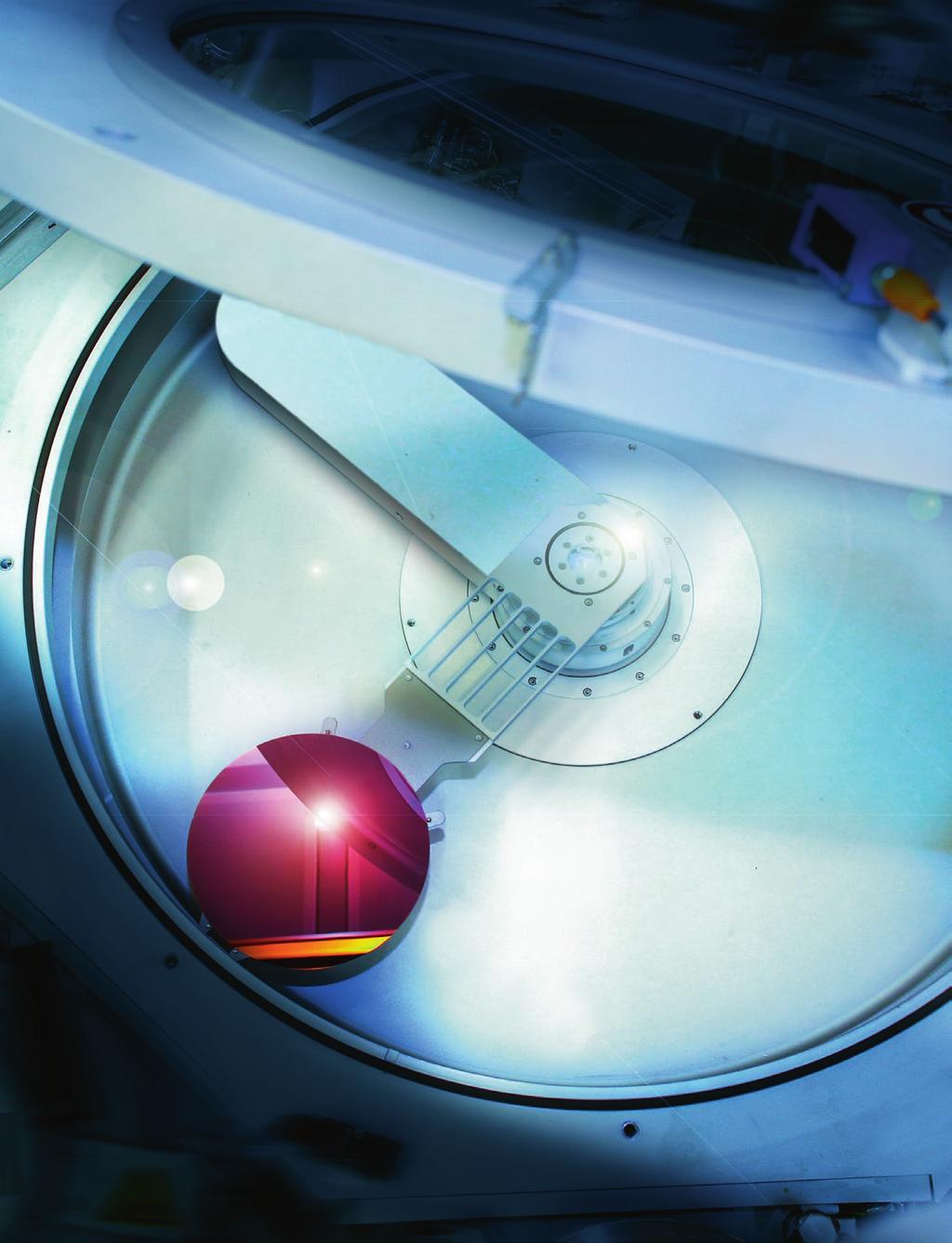
3 KEY FEATURES KEY COMPONENTS Based on the experience of more than 0 years in magnetron sputtering and over 50 years in evaporation, we have incorporated a broad scope of features into VON ARDENNE modular process systems. Our modular process systems use all the important vacuum thin-film technologies. Beyond that, they can also apply various pre- and post-treatment methods. On top of that, there are many options for monitoring, handling and control. You can see all the key features of our systems in more detail below. The success of our modular process systems is based on their highly flexible and broad configuration range, our technological experience and know-how, and on our in-house developed and manufactured key components. Depending on the required tool configuration, a VON ARDENNE system may include one or more of the listed components. Due to their modular design, the systems can also be upgraded or retrofitted with these components after the initial system installation. Single substrate Magazine Heating Degassing Etching (e-beam, glow discharge) PRE/POST TREATMENT HANDLING 5 Substrate flip station Carrier return system Mask Aligner 6 Automatic loading and unloading by industrial robots 7 Cleanroom compatible Glow discharge device LION ion source Sputtering, planar 5 Plasma-enhanced chemical vapor deposition (PECVD) Sputtering, confocal COATING PROCESSES 6 Atomic layer deposition (ALD) Sputtering with rotating magnet field 7 Hot wire Evaporation (thermal, E-beam) 8 Other process technologies on request Circular magnetron Rectangular magnetron Cylindrical magnetron VAprocos Process emission monitor (PEM) Pyrometer Deposition rate monitoring & control Temperature logger 5 MONITORING CONTROL Manual or fully automated working SECS / GEM interface Comprehensive process data logging User management Circular PECVD source VAprocos process control system Wicon control software


 Vertically adjustable,")


, which is able to deposit thin films with an")


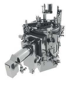
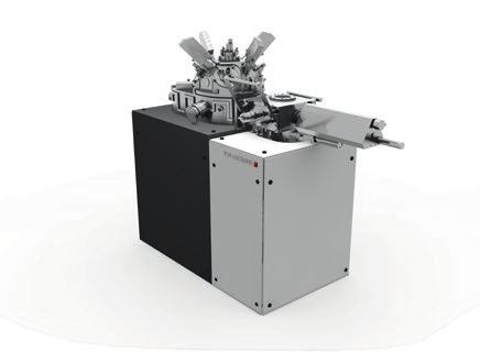


4 CLUSTER SYSTEMS MODULAR, FLEXIBLE & COST-EFFECTIVE Our cluster systems are based on a platform with many modular units. Therefore, every tool may be configured according to the specific applications of our customers. On top of that, special features can be integrated to meet the demand of the customer. Thanks to this flexibility, VON ARDENNE cluster systems help our customers to reduce their cost of ownership. REFERENCE SYSTEMS LOAD CHAMBERS LS500 THE COMPACT ALL-ROUNDER PRE-TREATMENT CHAMBERS Single substrate module POST-TREATMENT CHAMBERS The very compact system can be applied for the deposition of layer systems in research and development and in small-scale batch production. The up to four magnetrons of the system enable a highly flexible operation with various layer systems. Furthermore, the LS500 is suited for separate or co-sputtering. As these features can be combined with further options such as BIAS and monitoring systems, the LS500 is a true all-rounder. The substrates handling is wafer or carrier-based. Cleaning or etching module Magazine module TRANSFER CHAMBERS 6 ports 8 ports H passivation or flash module Load chamber Single substrate or magazine Process chamber Metals, oxides, alloys, e.g. focally arranged magnetrons barrier layers for medical applications (implants) Vertically adjustable, helium-cooled, rotatable substrate holder, suited for RF BIAS Heating or cooling system Process emission monitor (PEM), pyrometer CS500 HIPIMS CLUSTER SYSTEM The CS500 uses state-of-the-art coating technology - so-called high-power impulse magnetron sputtering (HIPIMS), which is able to deposit thin films with an extremely high density. It is especially designed for applications that require a high degree of precision such as coatings on glass to prevent glare or to produce more responsive smartphone screens and technology. ports PECVD ICP module Load chamber Magazine load lock for carriers 6-port transfer chamber Vacuum robot Pre-treatment chamber Sputter module, -fold, parallel (R)IBE/S PROCESS CHAMBERS Evaporation E-beam evaporator process chambers Hard substance and especially dense coatings CS00 MEMS CLUSTER SYSTEM Up to focally arranged magnetrons each Unbalanced high-power impulse magnetron sputtering (HIPIMS) Rotatable and vertically adjustable carrier platform Substrate heating (up to 900 C) Quick gas inlet and distribution system Monitoring systems (e.g. pyrometer) The CS00 is especially suited for the deposition of highly reflective layer systems for MEMS and MOEMS (micro(opto)electromechanical systems). These layer systems are, for instance, micromirror arrays tailored for industrial applications. Thanks to the cluster design of the CS00, several consecutive layers can be deposited in-situ, without removing the substrate from the vacuum. Sputter module, single, parallel The system enables coatings with exceptionally high precision with regards to layer quality. It also enables a long-term stable process and a quick sputter pressure control system. PECVD CCP module load chambers Wafer magazine load locks 8-port transfer chamber Vacuum robot and integrated aligner and cooler Pre-cleaning chamber 5 process chambers Metallization, highly reflective, anti-reflection (AR) and cover layers 00 mm high-power magnetrons with high uniformity and target utilization DC, DC pulsed and RF processes Sputter module, -fold confocal Hot-wire module


![Loading and unloading station Robot loading for one carrier Entry/exit load lock chamber Vacuum bypass line for fast evacuation Loading station [operated under air] Entry load lock chamber](/docs-images/82/85439258/images/5-3.jpg "Pre-treatment chamber The loading station is where the system is loaded manually with a carrier loaded with substrates or where substrates are placed on carriers, either manually or with the help of")


5 INLINE SYSTEMS HORIZONTAL OR VERTICAL HIGH-PRODUCTIVITY TOOLS For the processing of larger substrates at a higher productivity, VON ARDENNE provides several inline coating systems. We have delivered and installed such inline systems both in vertical and horizontal design. They are used for medium-scale production and for layer optimization by customers running our larger coating equipment, as the resulting process parameters can be easily transferred. REFERENCE SYSTEMS VISS SINGLE-END SPUTTER SYSTEM This system is suited for the large-area deposition of optical single or multiple metal or metal oxide layers. Thanks to its modular design, it can be equipped with a multitude of features. The substrates are transported through the system with a carrier, which is vertically tilted by -7. This arrangement reduces the contamination with particles and enables that the substrates can be loaded without touching their front side. Loading and unloading station Robot loading for one carrier Entry/exit load lock chamber Vacuum bypass line for fast evacuation Loading station [operated under air] Entry load lock chamber Pre-treatment chamber The loading station is where the system is loaded manually with a carrier loaded with substrates or where substrates are placed on carriers, either manually or with the help of a robot. Alternatively, a magazine loading station for several carriers can be used. The entry load lock chamber allows for the loading of the carrier without venting the process chambers of the system. Optionally, it can be equipped with a heating module or a bypass to reduce pumping time. Alternatively, a combined fore-vacuum/ highvacuum load lock with integrated pre-treatment can be used. The pre-treatment chamber can be fitted with an glow discharge device, inverse sputter etcher, LION ion source or a hollow cathode. Pre-treatment chamber Process chamber planar magnetrons Metals and oxides for optical DC, RF processes applications Gas inlet system VISS CONTINUOUS SPUTTER SYSTEM This system is designed as a truly continuous system for layer development under nearproduction conditions. However, it can also be used as a production tool for cold and hot reactive and non-reactive deposition processes. loading stations For one carrier load lock chambers Integrated heating module Pre-treatment chamber LION ion beam etching component Electron beam hollow cathode Heating module Process chamber 8 magnetrons, either planar or rotatable Al, CZT, MoOxNy, ZnTe - semiconductor materials, metals - Heating modules contact materials Highly precise temperature guidance PEM for reactive processes Cool trap Coating chambers The coating chambers are modularly configured and consist of a variable number of different process stations, depending on the customer requirements. Therefore, the modules can be connected in series accordingly. The available coating processes are sputtering and PECVD. Furthermore, thermal and electron beam evaporation can be applied in our horizontally configured systems. The process chambers can be used for reactive, partly-reactive, and non-reactive AC, DC or DC pulse deposition processes. For that, either standard VON ARDENNE planar single magnetron sputter sources, double arrangements of planar magnetrons or rotatable magnetron sputter sources are used. Additionally, heaters and cool traps can be integrated, or monitoring systems for controling the process or the deposited layer behavior. HISS HORIZONTAL OLED SYSTEM Exit load lock chamber The exit load lock chamber enables the unloading of the carrier without venting the process chambers of the system. Optionally, it can be fitted with a cooling module. Unloading station [operated under air] The unloading station is where the system is unloaded manually or by using a robot system. Alternatively, a magazine unloading station for several carriers can be used or the station can be combined with a carrier return system. The systems have a modular design and consist of stand-alone sections with process components arranged on mounting flanges. This allows for numerous configurable design options according to customer requirements. The coating process can be executed with nonmoving substrates (e.g. PECVD or evaporation processes) or oscillating substrates with continuously passing carriers. The coating cycles will vary strongly depending on the processes and the chosen equipment. All modules are suitable for /7 operation. In order to achieve highest productivity, the systems feature automatic (un)loading of the substrates, carrier return systems as well as SECS/GEM data interfaces for fab automation. This system is a production tool for manufacturing OLED (organic light emitting diodes) displays. A feature that makes this machine unique is the structured deposition with the help of two different masks. These masks are exchanged inside the vacuum. The system uses VON ARDENNE linear organic evaporation sources with inert material feed. The system is loaded and unloaded fully automatically and features a sophisticated carrier return system. loading and unloading stations Robot loading Mask positioning system entry/exit load lock chambers Integrated aligner and cooler 5 buffer chambers To guarantee high productivity process chambers OLED materials, contact metals Evaporation sources for organic and metallic deposition Co-evaporation Carrier and substrate centering Quartz rate, temperature, position monitoring Carrier return system In inert atmosphere


6 DRUM COATING SYSTEMS COMPACT, LOW-COST & PRODUCTIVE Drum coating systems have several advantages: They offer a quite high productivity and a compact footprint. They are also an affordable investment. Especially for alternating multilayer deposition, these systems are very powerful tools. In combination with pre-treatment, heating and cooling features and an inline deposition monitoring, a broad scope of applications can be targeted. We have highlighted two installed versions for you below. REFERENCE SYSTEMS BS00 SINGLE-CHAMBER DRUM COATING SYSTEM This system is designed as a single-chamber system for processing of up to 00 mm x 600 mm or 8-inch substrates by means of magnetron sputtering in DC processes. The substrates are accommodated in carriers. These carriers are arranged at the outside of a cylindrical basket. The basket rotates around a vertical axis within a vacuum chamber (rotary basket). A large door is used to load or unload the carrier with the substrates in and out of the process chamber. The door can be opened from a cleanroom while the system itself is installed in a gray room. Optionally, a loading/ unloading station can be integrated. Shutter systems in front of the magnetrons allow for pre-sputtering and for quickly stopping the deposition of material onto the substrates. Loading/unloading station Large door for loading/unloading Rotary basket Pre-treatment chamber Process chamber planar or rotatable magnetrons Short-wavelength mirrors BIAS CS00 MULTI-CHAMBER DRUM COATING SYSTEM High vacuum pumping system With turbopumps The CS00 is a -chamber system and enables the processing of customer-specific substrates by means of RF sputter etching, RF sputtering or unipolar DC or pulsed coating. This can be done in process mode with horizontally directed particle stream and vertically arranged substrates. The system enables hot deposition at a defined and highly uniform temperature. The system is loaded through a magazine load lock chamber. A vacuum robot transfers the carrier automatically between each vacuum chamber of the system. One of the of applications for this system is the manufacturing of thermo-electrical generators. Process chamber - Large door for loading/unloading stainless steel vacuum chamber with 5 ports User-friendly handling Up to magnetrons, planar or rotatable Easy to clean Pre-treatment module Loading/unloading station Magazine load lock chamber combined with loading/unloading door Transfer chamber Vacuum robot Carrier storage area For temporary storage in vacuum Rotary drum with several compartments for substrate carriers! Carrier size is defined by the substrate Freely selectable rotation speed Basket can be removed UPGRADE FOR HIGHER PRODUCTIVITY POSSIBLE Automatic loading/unloading Optical monitoring/process control PEM process chambers Semiconductors and metallic materials One for metallization, one for semiconductor materials and barrier films Simultaneous processing in both process chambers is possible Pre-cleaning with etching unit Up to 9 planar magnetrons Heating system PEM
7 REFERENCES PRODUCT TOPICS PRODUCT INDEX COMPONENTS VON ARDENNE WHO WE ARE & WHAT WE DO. VON ARDENNE develops and manufactures industrial equipment for vacuum coatings on materials such as glass, wafers, metal strip and polymer films. These coatings give the surfaces new functional properties and can be between one nanometer and a few micrometers thin, depending on the application. Our customers use these materials to make high-quality products such as architectural glass, absorbers and absorber tubes for solar-thermal power plants, refl ectors for lighting systems, displays for smartphones and touchscreens, solar modules and heat protection window film for automotive glass. We supply our customers with technologically sophisticated vacuum coating systems, extensive expertise and global service. The key components are developed and manufactured by VON ARDENNE itself. Systems and components made by VON ARDENNE make a valuable contribution to protecting the environment. They are vital for manufacturing products which help to use less energy or to generate energy from renewable resources. SALES CONTACTS SERVICE CONTACTS WORLDWIDE SALES AND SERVICE VON ARDENNE GmbH (headquarters) I Am Hahnweg 8 I 08 DRESDEN I GERMANY Sales: +9 (0) 5 67 I sales@vonardenne.biz Service: +9 (0) I support@vonardenne.biz VON ARDENNE Vacuum Equipment (Shanghai) Co., Ltd. I I I sales-vave@vonardenne.biz; support-vave@vonardenne.biz VON ARDENNE Malaysia Sdn. Bhd. I I I sales-vama@vonardenne.biz; support-vama@vonardenne.biz VON ARDENNE Japan Co., Ltd. I Tokyo office I I I sales-vajp@vonardenne.biz; support-vajp@vonardenne.biz VON ARDENNE Japan Co., Ltd. I Osaka office I I I sales-vajp@vonardenne.biz; support-vajp@vonardenne.biz VON ARDENNE North America, Inc. I Ohio office I I I sales-vana@vonardenne.biz; support-vana@vonardenne.biz VON ARDENNE North America, Inc. I Arizona office I I I sales-vana@vonardenne.biz; support-vana@vonardenne.biz Photos VON ARDENNE GmbH ENGLISH 0/07
EQUIPMENT EQUIPMENT FOR HIGH-EFFICIENCY SOLAR CONCEPTS CRYSTALLINE SILICON PV. SCALA XEA nova XENIA
 CRYSTALLINE SILICON PV EQUIPMENT EQUIPMENT FOR HIGH-EFFICIENCY SOLAR CONCEPTS SCALA XEA nova XENIA VON ARDENNE was founded in 1991 as a spin-off of the former Manfred von Ardenne Research Institute. The
Photovoltaics & Solar Thermals. Thin-film equipment. Customized. FHR Anlagenbau GmbH I
 Photovoltaics & Solar Thermals Thin-film equipment. Customized. FHR Anlagenbau GmbH I www.fhr.de FHR Anlagenbau GmbH is an innovative enterprise in the branch of vacuum processing and thin-film technologies.
Power Vision Ltd. PV Research. Power Vision Ltd. Unit R2, Herald Park, Crewe, Cheshire, CW1 6EA, UK Tel:
 Power Vision Ltd PV Research Power Vision Ltd Unit R2, Herald Park, Crewe, Cheshire, CW1 6EA, UK www.pvoptical.com Tel: +44 1270 253000 Flexible Whether it be fast AR coating onto temperature sensitive
SPUTTERING TECHNOLOGY. for Multiple Applications such as Solar, Display, Semiconductor & 3D-Substrates
 SPUTTERING TECHNOLOGY for Multiple Applications such as Solar, Display, Semiconductor & 3D-Substrates 02 Over 20 Years of Know-how in Physical Vapor Deposition Sputtering PECVD Evaporation SINGULUS TECHNOLOGIES
Linear Plasma Sources for Surface Modification and Deposition for Large Area Coating
 Linear Plasma Sources for Surface Modification and Deposition for Large Area Coating Dr Tony Williams Gencoa Ltd, UK Victor Bellido-Gonzalez, Dr Dermot Monaghan, Dr Joseph Brindley, Robert Brown SVC 2016,
Inline Sputtering System for Heterojunction Cells
 GENERIS PVD Inline Sputtering System for Heterojunction Cells GENERIS PVD Inline Sputter System for ITO and Ag Deposition on Heterojunction Solar Cells Sputtering Technology at a Glance has delivered far
Si DRIE APPLICATION In Corial 210IL
 Si DRIE APPLICATION In Corial 210IL CORIAL 210IL ICP-RIE equipment for deep Si etching applications Enlarged functionality with capability to deep etch silicon, silicon carbide, glass, sapphire, and quartz
BAK. Evaporator Family
 BAK Evaporator Family The BAK A new generation Taking the best from the past, expanding your horizons for the future! More than 1500 systems worldwide 2 BAK Evaporator Family more choice than ever Welcome
BAK EVAPORATOR FAMILY
 BAK EVAPORATOR FAMILY THE BAK A NEW GENERATION TAKING THE BEST FROM THE PAST, EXPANDING YOUR HORIZONS FOR THE FUTURE! The BAV 2000 - a production giant 2000 BAK SYSTEMS DELIVERED WORLDWIDE 2 BAK EVAPORATOR
PlasmaPro TM System100 & System133. Modular tools for wafer processing100
 TM System100 & System133 Modular tools for wafer processing100 System100 & System133 Plasma etch & deposition process modules Oxford Instruments System100 and System133 process modules are built on 200mm
Microwave Plasma Processing
 Microwave Plasma Processing MUEGGE GMBH Hochstraße 4-6 64385 Reichelsheim Fon +49 (0) 6164-93 07 11 Fax +49 (0) 6164-93 07 93 info@muegge.de www.muegge.de Microwave Plasma Processing Microwave Plasma Technology:
BAK EVAPORATOR FAMILY
 BAK EVAPORATOR FAMILY THE BAK A NEW GENERATION TAKING THE BEST FROM THE PAST, EXPANDING YOUR HORIZONS FOR THE FUTURE! The BAV 2000 - a production giant 2000 BAK SYSTEMS DELIVERED WORLDWIDE 2 BAK EVAPORATOR
1 Introduction. 2 Basic Technology
 Innovative Clear Barrier Technology for the Packaging Industry Nicolas Schiller 1, Steffen Straach, Steffen Günther Fraunhofer FEP, Germany Alexandra L. Quiceno G., Antonio García Contreras BIOFILM, Columbia
PEAK EFFICIENCIES WITH FALLING MANUFACTURING COSTS
 PEAK EFFICIENCIES WITH FALLING MANUFACTURING COSTS Simple and cost-effective introduction of PERC technology into the mass production of solar cells Kerstin Strauch, Florian Schwarz, Sebastian Gatz 1 Introduction
Semiconductor Device Fabrication
 5 May 2003 Review Homework 6 Semiconductor Device Fabrication William Shockley, 1945 The network before the internet Bell Labs established a group to develop a semiconductor replacement for the vacuum
Plasma Activated EB-PVD of Titanium and its Compounds by Means of Large Area SAD
 AIMCAL 2005 Myrtle Beach, SC, USA, October 19th, 2005 Plasma Activated EB-PVD of Titanium and its Compounds by Means of Large Area SAD E. Reinhold, C. Steuer VON ARDENNE Anlagentechnik GmbH, Dresden, Germany
Chapter 3 Silicon Device Fabrication Technology
 Chapter 3 Silicon Device Fabrication Technology Over 10 15 transistors (or 100,000 for every person in the world) are manufactured every year. VLSI (Very Large Scale Integration) ULSI (Ultra Large Scale
Transactions on Engineering Sciences vol 2, 1993 WIT Press, ISSN
 A study of thin-film continuous coating process by vapour deposition P. Gimondo," F. Arezzo,* B. Grifoni,* G. Jasch& "Centra Sviluppo Materiali SpA, Via di Castel & Von Ardenne Anlagentchnik GmbH, Plattleite
On the way to the latest packaging R2R Metallizer
 On the way to the latest packaging R2R Metallizer AIMCAL FALL Conference 2011 Schmid Vacuum Technology GmbH, Karlstein, Germany Peter Sauer Gerard Löbig Andre Herzog Johannes Krantz Michael Klosch-Trageser
High Performance Optical Coatings Deposited Using Closed Field Magnetron Sputtering
 High Performance Optical Coatings Deposited Using Closed Field Magnetron Sputtering D.R. Gibson, I.T. Brinkley, and J.L. Martin Applied Multilayers LLC, 1801 SE Commerce Avenue, Battle Ground, WA 98604
MAGNION Series Sputter Deposition Systems and Cathodes
 Advancing Plasma-Based Technologies PLASMIONIQUE À l Avant-Garde des Technologies Plasma MAGNION Series Sputter Deposition Systems and Cathodes MAGNION Series of Sputter Deposition systems offer Turnkey
Plasma Quest Limited
 Plasma Quest Limited A Remote Plasma Sputter Process for High Rate Web Coating of Low Temperature Plastic Film with High Quality Thin Film Metals and Insulators Dr. Peter Hockley and Prof. Mike Thwaites,
Mass Production of Clear Barriers. Requirements on Vacuum Web Coaters for Quality Assurance. Rainer Ludwig, Applied Films, Alzenau, Germany.
 Mass Production of Clear Barriers Requirements on Vacuum Web Coaters for Quality Assurance Rainer Ludwig, Applied Films, Alzenau, Germany Abstract An increasing number of packages using Transparent Barrier
MODEL SEM Mill. Two independently adjustable TrueFocus ion sources
 MODEL 1060 SEM Mill A state-of-the-art ion milling and polishing system. It is compact, precise, and consistently produces high-quality scanning electron microscopy (SEM) samples for a wide variety of
MODEL 1061 SEM Mill ION MILLING. Ion milling is used in the physical. sciences to enhance the sample s surface. characteristics. Inert gas, typically
 MODEL 1061 SEM Mill A state-of-the-art ion milling and polishing system. It is compact, precise, and consistently produces high-quality scanning electron microscopy (SEM) samples in the shortest amount
Applied Research for Vacuum Web Coating: What is Coming Next?
 Applied Research for Vacuum Web Coating: What is Coming Next? Matthias Fahland, John Fahlteich, Steffen Günther, Manuela Junghähnel, Claus Luber, Nicolas Schiller, Cindy Steiner, Steffen Straach, Michiel
Activities in Plasma Process Technology at SENTECH Instruments GmbH, Berlin. Dr. Frank Schmidt
 Activities in Plasma Process Technology at SENTECH Instruments GmbH, Berlin Dr. Frank Schmidt The Company Company Private company, founded 1990 80 employees ISO 9001 Location Science & Technology Park,
GENERIS PVD. Inline Sputtering System for Heterojunction Solar Cells
 GENERIS PVD Inline Sputtering System for Heterojunction Solar Cells GENERIS PVD Inline Sputtering System for Heterojunction Solar Cells Sputtering Competence has delivered far more than 8000 vacuum sputtering
Non-contractual document, specifications subject to change without notice.
 1 ANNEALSYS designs and manufactures Rapid Thermal Processing (RTA, RTCVD) Direct Liquid Injection (DLI-CVD, DLI-ALD) systems for research laboratories and companies for semiconductor, MEMS, nanotechnologies,
Advanced Glass Refinement by Thin Films - Trends and Challenges of Thin Film Technologies for Windows and Facade Glasses
 Advanced Glass Refinement by Thin Films - Trends and Challenges of Thin Film Technologies for Windows and Facade Glasses Dr.-Ing. Manuela Junghähnel Fraunhofer Institute for Elect ron Beam and Plasma Technology
MODEL 1051 TEM Mill ION MILLING. Ion milling is used on physical science. specimens to reduce thickness to electron
 MODEL 1051 TEM Mill A state-of-the-art ion milling and polishing system offering reliable, high performance specimen preparation. It is compact, precise, and consistently produces high-quality transmission
High Rate Deposition of Reactive Oxide Coatings by New Plasma Enhanced Chemical Vapor Deposition Source Technology
 General Plasma, Inc. 546 East 25th Street Tucson, Arizona 85713 tel. 520-882-5100 fax. 520-882-5165 High Rate Deposition of Reactive Oxide Coatings by New Plasma Enhanced Chemical Vapor Deposition Source
Corial PS200 4-sided multi-module platform
 Corial PS200 4-sided multi-module platform Single wafer platform equipped with 200 mm modules Integration of ICP-CVD or PECVD process chambers Fully automated platform with cassette-to-cassette handler
GENCOA. Perfect your process
 GENCOA Perfect your process 02 Introduction Providing expert solutions to a worldwide customer base over three decades, Gencoa is among the world leaders in the design and manufacture of products for the
AMOLED DISPLAY PROTOTYPING SYSTEM CLUSTER TYPE FMM TECHNOLOGY
 IIT Madras NOVEMBER 2, 2018 SPECIFICATIONS DOCUMENT IITM_FMM_01 AMOLED DISPLAY PROTOTYPING SYSTEM CLUSTER TYPE FMM TECHNOLOGY Department of Electrical Engineering, IIT MADRAS Contents 1. Cluster-Style
Physical Vapor Deposition (PVD) Zheng Yang
 Zheng Yang") Physical Vapor Deposition (PVD) Zheng Yang ERF 3017, email: yangzhen@uic.edu Page 1 Major Fabrication Steps in MOS Process Flow UV light Mask oxygen Silicon dioxide photoresist exposed photoresist oxide
Physical Vapor Deposition (PVD) Zheng Yang ERF 3017, email: yangzhen@uic.edu Page 1 Major Fabrication Steps in MOS Process Flow UV light Mask oxygen Silicon dioxide photoresist exposed photoresist oxide
Extending product lifetime with ALD moisture barrier
 Whitepaper Extending product lifetime with ALD moisture barrier 01 executive summary Atomic Layer Deposition (ALD) is a thin film technology that enables new and highly competitive products. Typical applications
EE 5344 Introduction to MEMS. CHAPTER 3 Conventional Si Processing
 3. Conventional licon Processing Micromachining, Microfabrication. EE 5344 Introduction to MEMS CHAPTER 3 Conventional Processing Why silicon? Abundant, cheap, easy to process. licon planar Integrated
Intlvac Nanochrome I Sputter System (intlvac_sputter)
") 1. Intlvac_Sputter Specifications The Intlvac Nanochrome I sputter system is configured for DC, AC (40 khz), and RF (13.56 MHz) magnetron sputtering. They system has in-situ quartz lamp heating up to 200C,
1. Intlvac_Sputter Specifications The Intlvac Nanochrome I sputter system is configured for DC, AC (40 khz), and RF (13.56 MHz) magnetron sputtering. They system has in-situ quartz lamp heating up to 200C,
Turn-key Production System for Solar Cells
 SOLARE Turn-key Production System for Solar Cells 02 Innovations for New Technologies provides technology solutions for both crystalline and thin-film highperformance solar cell platforms. Our production
A Basic Introduction to Thin-Film Coatings. From the Experts at VaporTech
 A Basic Introduction to Thin-Film Coatings From the Experts at VaporTech What are thin-film coatings? 2018 Vapor Technologies, Inc. All rights reserved. Thin-film coatings Physical or Chemical Vapor Deposition
Model TEM Mill. Tabletop precision preparation for producing high-quality TEM specimens from a wide variety of materials EXCELLENCE MAGNIFIED
 Model 1050 TEM Mill Tabletop precision preparation for producing high-quality TEM specimens from a wide variety of materials EXCELLENCE MAGNIFIED Modular design for basic instrument operation or fully
CeraTHERM stack. Clean room-compatible thermal systems with stacking technology. Thermal systems
 CeraTHERM stack Clean room-compatible thermal systems with stacking technology EN Thermal systems 2 CeraTHERM stack Clean room-compatible stack systems The vertical stack systems from CeraCon are extremely
ise J. A. Woollam Ellipsometry Solutions
 ise J. A. Woollam Ellipsometry Solutions Capabilities The ise is a new in-situ spectroscopic ellipsometer developed for real-time monitoring of thin film processing. Using our proven technology, the ise
Magnetron Sputter Cathodes planar & rotatable. Linear ion sources. Reactive gas controller & endpoint detector
 GENCOA products cover 3 sputtering related areas Magnetron Sputter Cathodes planar & rotatable Reactive gas controller & endpoint detector Linear ion sources Other activities include on-site process implementation,
Metallization deposition and etching. Material mainly taken from Campbell, UCCS
 Metallization deposition and etching Material mainly taken from Campbell, UCCS Application Metallization is back-end processing Metals used are aluminum and copper Mainly involves deposition and etching,
HiPace Turbopumps. Innovation HiPace TM. The new Dimension in Vacuum Technology! Intelligent. Flexible. Efficient. YEARS TURBO 50PUMPS
 HiPace Turbopumps Innovation HiPace TM The new Dimension in Vacuum Technology! Intelligent. Flexible. Efficient. YEARS TURBO 50PUMPS HiPace Turbopumps Innovation HiPace TM Ever wonder why all turbopumps
Lecture Day 2 Deposition
 Deposition Lecture Day 2 Deposition PVD - Physical Vapor Deposition E-beam Evaporation Thermal Evaporation (wire feed vs boat) Sputtering CVD - Chemical Vapor Deposition PECVD LPCVD MVD ALD MBE Plating
CLUSTERLINE A family of 200 & 300mm cluster tools for Advanced Packaging, Power Devices, MEMS and Optoelectronics
 A family of 200 & 300mm cluster tools for Advanced Packaging, Power Devices, MEMS and Optoelectronics THREE REASONS TO CHOOSE 1 PROVEN PLATFORM RELIABILITY is a high volume single wafer processing production
Pioneering ALD experience since The ALD Powerhouse PRODUCT CATALOGUE FOR SUNALE P-SERIES ALD SYSTEMS
 Pioneering ALD experience since 1974 The ALD Powerhouse PRODUCT CATALOGUE FOR SUNALE P-SERIES ALD SYSTEMS SUNALE P-SERIES ALD SYSTEMS PRODUCT CATALOGUE Description SUNALE P-series ALD system SUNALE P-series
Ion-plasma technologies and equipment
 Ion-plasma technologies and equipment VACUUM ION-PLASMA INSTALLATIONS OF «OPAL» SERIES «Opal» series ion-plasma installations are designed for deposition of low-emission, reflective and toned coatings
MODEL TEM Mill. Two independently adjustable TrueFocus ion sources
 MODEL 1050 TEM Mill A state-of-the-art ion milling and polishing system. It is compact, precise, and consistently produces high-quality transmission electron microscopy (TEM) specimens with large electron
Gencoa Product Portfolio
 Gencoa offer the following range of products & process technology for the thin film industry developed over the last 20 years Planar Magnetrons Plasma Pre- Treaters Reactive Gas Controllers Gencoa Product
Thermal Evaporation. Theory
 Thermal Evaporation Theory 1. Introduction Procedures for depositing films are a very important set of processes since all of the layers above the surface of the wafer must be deposited. We can classify
WHEN THIN FILM MATTERS PVD SYSTEMS.
 WHEN THIN FILM MATTERS PVD SYSTEMS www.polyteknik.com WHEN THIN FILM MATTERS POLYTEKNIK AS Polyteknik AS is a PVD equipment manufacturer with an innovative and best service approach. With more than twenty
Previous Lecture. Vacuum & Plasma systems for. Dry etching
 Previous Lecture Vacuum & Plasma systems for Dry etching Lecture 9: Evaporation & sputtering Objectives From this evaporation lecture you will learn: Evaporator system layout & parts Vapor pressure Crucible
Decorative Coatings PVD the bright choice
 a parent company of Decorative Coatings PVD the bright choice kenosistec.com a parent company of Why PVD Coating Best surface properties PVD is still one of the most effective method for modifying and
General Introduction to Microstructure Technology p. 1 What is Microstructure Technology? p. 1 From Microstructure Technology to Microsystems
 General Introduction to Microstructure Technology p. 1 What is Microstructure Technology? p. 1 From Microstructure Technology to Microsystems Technology p. 9 The Parallels to Microelectronics p. 15 The
From Vacuum to Atmosphere and back an in-house Process Chain for Different Products
 From Vacuum to Atmosphere and back an in-house Process Chain for Different Products Dr. Steffen Günther Vacuum coating low pressure 10-1 10-4 Pa (10-3 10-6 mbar) unhindered particle movement no unintended
Low temperature deposition of thin passivation layers by plasma ALD
 1 Low temperature deposition of thin passivation layers by plasma ALD Bernd Gruska, SENTECH Instruments GmbH, Germany 1. SENTECH in brief 2. Low temperature deposition processes 3. SENTECH SI ALD LL System
csi PRODUCTION SOLUTIONS csi PRODUCTION SOLUTIONS FOR CRYSTALLINE SILICON SOLAR CELLS
 csi PRODUCTION csi PRODUCTION FOR CRYSTALLINE SILICON SOLAR CELLS 3 PASSION FOR EFFICIENCY PHOTOVOLTAICS CONTENT Process machines and automation systems by Manz offer many advantages for customers in the
Plasma-Enhanced Chemical Vapor Deposition
 Plasma-Enhanced Chemical Vapor Deposition Steven Glenn July 8, 2009 Thin Films Lab 4 ABSTRACT The objective of this lab was to explore lab and the Applied Materials P5000 from a different point of view.
EQUIPMENT AND SYSTEM FOR VACUUM COATING METALLIZING, SPUTTERING, PLASMA and PECVD. Hybrid system KOLZER DGK 36
 email : carlo.gennari@fastwebnet.it web site : http://carlogennariforni.beepworld.it/kolzer.htm EQUIPMENT AND SYSTEM FOR VACUUM COATING METALLIZING, SPUTTERING, PLASMA and PECVD Hybrid system KOLZER DGK
Denton 635 Sputter SOP
 Denton 635 SOP Page 1 of 8 Denton 635 Sputter SOP 1. Scope 1.1 This document provides operating procedures for the Denton 635 automated sputter system.. 2. Table of Contents 1. Scope... 1 2. Table of Contents...
Solar absorber coatings
 Solar absorber coatings Maximum output Solar thermal collectors use energy from the sun to generate heat for heating and hot water. This energy is free, environmentally friendly and reliable. The heart
Managing Anode Effects and Substrate Heating from Rotatable Sputter Targets
 Managing Anode Effects and Substrate Heating from Rotatable Sputter Targets Frank Papa*, Dermot Monaghan**, Victor Bellido- González**, and Alex Azzopardi** *Gencoa Technical & Business Support in US,
Productivity versus Profitability in Vacuum Web Coating
 Productivity versus Profitability in Vacuum Web Coating Liz Josephson, Applied Films Corp., Longmont, USA Dirk Hoffmann, Applied Films GmbH & Co KG, Alzenau, Germany Gerard Loebig, Applied Films GmbH &
CORIAL D500. Large capacity batch system for 24/7 production environment
 CORIAL D500 Large capacity batch system for 24/7 production environment High-quality films for a wide range of materials, incl. SiO2, Si3N4, SiOCH, SiOF, SiC and asi-h films Film deposition from 120 C
Preface Preface to First Edition
 Contents Foreword Preface Preface to First Edition xiii xv xix CHAPTER 1 MEMS: A Technology from Lilliput 1 The Promise of Technology 1 What Are MEMS or MST? 2 What Is Micromachining? 3 Applications and
Roll-to-roll Technology for Transparent High Barrier Films
 Roll-to-roll Technology for Transparent High Barrier Films Presented at the AIMCAL Fall Technical Conference, October 19-22, 2008, Myrtle Beach, SC, USA Nicolas Schiller, John Fahlteich, Matthias Fahland,
Nucleation and growth of nanostructures and films. Seongshik (Sean) Oh
 Oh") Nucleation and growth of nanostructures and films Seongshik (Sean) Oh Outline Introduction and Overview 1. Thermodynamics and Kinetics of thin film growth 2. Defects in films 3. Amorphous, Polycrystalline
Nucleation and growth of nanostructures and films Seongshik (Sean) Oh Outline Introduction and Overview 1. Thermodynamics and Kinetics of thin film growth 2. Defects in films 3. Amorphous, Polycrystalline
Corial D500 No mechanical cleaning
 Corial D500 No mechanical cleaning Large capacity batch system for 24/7 production environment High-quality films for a wide range of materials, incl. SiO2, Si3N4, SiOCH, SiOF, SiC and asi-h films Film
Efficient Production Technology and Process Automation
 Efficient Production Technology and Process Automation Since 1989, the Jonas & Redmann Group has been developing and producing intelligent automation solutions for handling, transport, and assembly. Our
ITO SPUTTER COATED FILMS FOR TOUCH PANEL APPLICATIONS USING ROTARY SINTERED CERAMIC ITO TARGETS: WHAT CAN BE LEARNED FROM GLASS COATING?
 ITO SPUTTER COATED FILMS FOR TOUCH PANEL APPLICATIONS USING ROTARY SINTERED CERAMIC ITO TARGETS: WHAT CAN BE LEARNED FROM GLASS COATING? Paul Lippens AIMCAL Web coating conference 2012 Outline Introduction
AC : MICROWAVE PLASMA CLEANER DESIGN FOR SEMI- CONDUCTOR FABRICATION AND MATERIALS PROCESSING LABO- RATORY USE
 AC 2011-2416: MICROWAVE PLASMA CLEANER DESIGN FOR SEMI- CONDUCTOR FABRICATION AND MATERIALS PROCESSING LABO- RATORY USE Mustafa G. Guvench, University of Southern Maine Mustafa G. Guvench received M.S.
The laser efficiency. primapower.com. The Bend The Combi The Laser The Punch The System The Software
 primapower.com The laser efficiency The Bend The Combi The Laser The Punch The System The Software 104GB/Apr2012 Prima Industrie Group / Subject to changes without prior notice Innovative and reliable
Atomic Layer Deposition. ALD process solutions using FlexAL and OpAL
 Atomic Layer Deposition process solutions using FlexAL and OpAL Introduction to Self limiting digital growth Atomic Layer Deposition () offers precisely controlled ultra-thin films for advanced applications
INFOVION S MAIN PRODUCTS
 INFOVION S MAIN PRODUCTS CONTENTS Cluster Sputter System Multi Cathode Sputter System Combinatorial IBSD System Combinatorial Sputter System IBSD System Roll Coating Sputter System RTA System MOCVD System
Solar absorber coatings
 Solar absorber coatings Maximum output Solar thermal collectors use energy from the sun to generate heat for heating and hot water. This energy is free, environmentally friendly and reliable. The heart
Electron beam technology for turbine coating
 Второй международный технологический форум "Инновации. Технологии. Производство." 23-25 марта 2015 года Electron beam technology for turbine coating Anastasiya Zagorni, MBA Prof. Dr. Christoph Metzner,
Plastic Electronics Precise and productive automation solutions
 Plastic Electronics Precise and productive automation solutions 2 Plastic Electronics Flexible electronics "off the roll" Today s electronics industry faces constant challenges as resource and energy costs
TFS PRODUCTION SOLUTIONS. TFS Production Solutions. For thin-film solar modules
 TFS PRODUCTION SOLUTIONS TFS Production Solutions For thin-film solar modules 2 TFS PRODUCTION SOLUTIONS MANZ AG 3 TFS PRODUCTION SOLUTIONS MANZ AG GERMAN ENGINEERING INTERNATIONALLY STAGED GLOBAL REFERENCES
Innovative Laser Processing Technologies
 Innovative Laser Processing Technologies Reinhard Ferstl Director Sales & Marketing EMEA / Asia Corning Laser Technologies September 21, 2016 2016 Corning Incorporated Corning Market Segments and Additional
Thermal Load And Heat Transfer Regarding EBPVD Of Plastic Web And Thin Metal Foils
 Thermal Load And Heat Transfer Regarding EBPVD Of Plastic Web And Thin Metal Foils J. Richter, E. Reinhold, Chr. Steuer VON ARDENNE Anlagentechnik GmbH D-01324 Dresden, Germany 1 - Thema - 12.08.2003 e-mail:
2 Boar s Head Lane Charlottesville, VA Phone Fax
 2 Boar s Head Lane Charlottesville, VA 22903 Phone 434-977-1405 Fax 434-977-1462 www.directedvapor.com DVTI has recently built DVD III, a fully operational production capable coater. This invaluable addition
FABRICATION ENGINEERING MICRO- NANOSCALE ATTHE AND. Fourth Edition STEPHEN A. CAMPBELL. of Minnesota. University OXFORD UNIVERSITY PRESS
 AND FABRICATION ENGINEERING ATTHE MICRO- NANOSCALE Fourth Edition STEPHEN A. CAMPBELL University of Minnesota New York Oxford OXFORD UNIVERSITY PRESS CONTENTS Preface xiii prrt i OVERVIEW AND MATERIALS
Manipulation and control of spatial ALD layers for flexible devices. Aimcal Memphis 2016; Edward Clerkx
 Manipulation and control of spatial ALD layers for flexible devices Meyer Burger Netherlands Equipment manufacturer Functional inkjet printing Based in Eindhoven, the Netherlands Part of world-wide Meyer
High Rate low pressure PECVD for barrier and optical coatings
 High Rate low pressure PECVD for barrier and optical coatings, Matthias Fahland, John Fahlteich, Björn Meyer, Steffen Straach, Nicolas Schiller Outline Introduction PECVD New developments magpecvd arcpecv
A Design for an efficient cylindrical magnetron cathode with rotating magnets and optical emission incorporated
 Patent on, A Design for an efficient cylindrical magnetron cathode with rotating magnets and optical emission incorporated Inventors A. Subrahmanyam, Krishna Valleti IIT Madras, Chennai, INDIA. Shrikanth
ALD Vacuum Technologies High Tech is our Business. Vacuum heat treatment system with high pressure gas quenching
 ALD Vacuum Technologies High Tech is our Business Vacuum heat treatment system with high pressure gas quenching High tech is our business ALD is a brand name associated world-wide with innovative vacuum
Solar Selective Absorber Coating Methods Plasma Processes
 Solar Selective Absorber Coating Methods Plasma Processes Paul Gantenbein & Elimar Frank SPF - Institut für Solartechnik University of Applied Sciences Rapperswil (HSR) Optical properties of a selective
MODEL Plasma Cleaner. Simultaneously cleans specimen and specimen holder. Cleans highly contaminated specimens in 2 minutes or less
 MODEL 1020 Plasma Cleaner Cleans specimens immediately before they are inserted into the electron microscope; removes existing carbonaceous debris from the specimen and prevents contamination from occurring
Linear Broad Beam Ion Sources ACC-30x150 IS, ACC-40x300 IS and ACC-40 x 600 IS
 Dr. Hermann Schlemm Ion Beam- and Surface Technology Saalbahnhofstraße 6 D - 07743 JENA, Germany Tel.: ++ 49 3641 22 73 29 Fax: ++ 49 3641 22 87 60 email: hermann.schlemm@jenion.de http://www.jenion.de
Photovoltaics. Thin film equipment from Oxford Instruments. The Business of Science
 Photovoltaics Thin film equipment from Oxford Instruments The Business of Science Photovoltaics Plasmalab System100Pro and Plasmalab System133Pro Flexible systems for front end PV research With over 20
Gridless end-hall. Ion Sources. For Ion Assisted Thin Film Deposition & Substrate Cleaning
 Gridless end-hall Ion Sources For Ion Assisted Thin Film Deposition & Substrate Cleaning End-Hall Ion Sources mark I Ion Source The Mark I End-Hall is ideal for small research and development and pilot
The Thin-Film Experts MAKE GREAT PRODUCTS EVEN BETTER WITH VAPORTECH THIN-FILM DEPOSITION SYSTEMS
 The Thin-Film Experts MAKE GREAT PRODUCTS EVEN BETTER WITH VAPORTECH THIN-FILM DEPOSITION SYSTEMS { Thin-Film Deposition / THin, film depә zish(ә) n/ DEFINED A vacuum process using an energy source to
Atomic Layer Deposition (ALD)
") Atomic Layer Deposition (ALD) ALD provides Uniform, controlled, conformal deposition of oxide, nitride, and metal thin films on a nanometer scale. ALD is a self limiting thin film deposition technique
Atomic Layer Deposition (ALD) ALD provides Uniform, controlled, conformal deposition of oxide, nitride, and metal thin films on a nanometer scale. ALD is a self limiting thin film deposition technique
TFS PRODUCTION SOLUTIONS. TFS Production Solutions. For thin-film solar modules
 TFS PRODUCTION SOLUTIONS TFS Production Solutions For thin-film solar modules 2 TFS PRODUCTION SOLUTIONS MANZ AG 3 TFS PRODUCTION SOLUTIONS MANZ AG GERMAN ENGINEERING INTERNATIONALLY STAGED GLOBAL REFERENCES
Q150R Series Rotary Pumped Coaters
 Q u o r u m Te c h n ologies Q150R Modular Coating Systems Q Series Rotary Pumped Coating Systems Innovative and versatile sputter High vacuum sputtering and carbon coater and carbonfor evaporator evaporation