Presentation Outline. Plasma Surface Modification Plasmas for Fabricating PV Cells PV Cell Fabrication Trend. Modification Effects
|
|
|
- Stephen Miller
- 6 years ago
- Views:
Transcription


1
2


3 Reducing Solar Module Cost with Atmospheric Plasma Surface Modification A Green Technology Presented by Rory A. Wolf, V.P. Enercon Industries Corporation
4 Presentation Outline Plasma Surface Modification Plasmas for Fabricating PV Cells PV Cell Fabrication Trend Atmospheric (Dry) Plasma Surface (APT) Modification Effects PV Cell Surface Preparation & Cleaning APT Prescriptions for PV Materials Conclusions
5 Plasma Surface Modification Plasma surface modification technology in PV cell manufacturing: o Deposition of amorphous SiN layers o Utilize vacuum PECVD process Create anti-reflection and surface passivation on thin-film solar cells V l hi i b l Vacuum plasma etching in barrel-type reactors for edge isolation
6 Plasma Surface Modification Increasing chemical waste disposal issues New interest in plasma systems o dry etching o surface cleaning o adhesion promotion Warrants fresh investigation of efficiencies
7 Plasmas for Fabricating PV Cells Use of plasmas dependent upon PV materials and cycle time Vacuum plasmas not a bridge to high volume continuous process SiNx deposition typically batch processes Can work in semi-continuous mode by exchanging materials after treatment and return to one atmosphere Not economical for high throughput etching cleaning and Not economical for high throughput etching, cleaning and functionalizing
8 PV Cell Fabrication Trends
9 PV Cell Fabrication Trends Organic Thin-Film Solar Cells on Plastic Organic semiconductive materials are dissolved in solvents or inks and printed or coated onto a plastic substrate in a continuous roll-to-roll process. Less expensive than silicon, cadmium or tellurium Prototypes in production now. Example 1: clear plastic top layer, a coating of prepolymer adhesive, then ink containing fullerene conductive nano-carbon clusters, and another liquid polymer coating, applied to PET film with an SiOx coating. Example 2: Use of organic inks for solar sells. The ink lets electrons pass to an electrically conductive polymer layer on a plastic substrate.
10 PV Cell Fabrication Trends Wide range of materials being examined to maximize solar efficiencies. Opportunity integrate continuous in-line processes for rigid/flexible PV cells Utilize atmospheric (gas phase) variable chemistry surface modification technology for dissimilar materials to improve fabrication efficiency.

11 Atmospheric Plasma Surface Modification
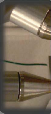
12 Atmospheric Plasma Surface Modification plasma : n ; Fourth state of matter, (Solid, Liquid, Gas, Plasma.) Mixture of charged ions & energetic electrons generally in equilibrium.
13 Atmospheric Plasma Surface Modification
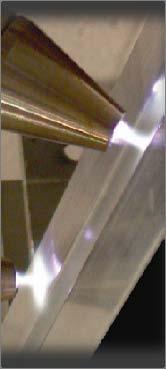
14 Atmospheric Plasma Surface Modification Recipe 1) Take one photon, and allow it to randomly liberate one bound electron from a gas molecule. 2) Accelerate this free electron in an electrical field, forcing it to collide with other gas molecules with enough kinetic energy to separate the atoms, or free more electrons. 3) Increase power in the electric field to create an avalanche of electron collisions.

15 Atmospheric Plasma Surface Modification
16 Atmospheric Plasma Surface Modification Plasma Activation Changes free radicals on the surface by substituting chemical groups on the polymer chain being modified. Plasma Deposition Hydroxyl, carbonyl, carboxyl, carboxylic, amino-carboxyl, and amine chemical groups on surface Plasma-Induced Grafting Free radicals are created along the polymer backbone.


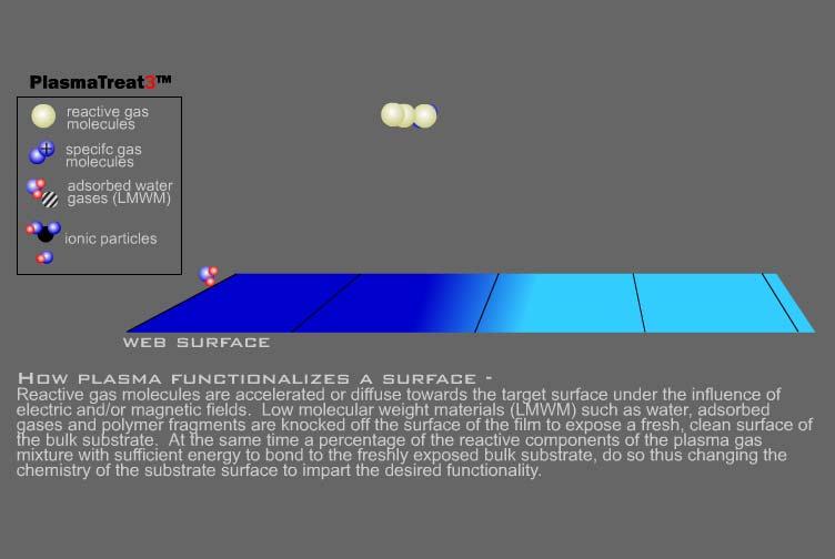
17 Atmospheric Plasma Surface Modification Animation demonstrates only one of the possible reaction pathways during plasma chemical oxidation of polyolefins. Reaction initiated with atomic oxygen, which abstracts an hydrogen atom from the surface. Results in a free radical on the surface, which can react with an oxygen molecule to produce a hydroperoxide group, which can decay into a keton group. Source: Fraunhofer IGB
 Specific surface functionalization possible under precise control of the")
18 Atmospheric Plasma Surface Modification Besides keton groups, also formed aldehyd, carboxyl, hydroperoxide, hydroxide, and ester groups (above). Plasma oxidation results in breaking the polymer chains and material removal (ablation) Specific surface functionalization possible under precise control of the reaction conditions.


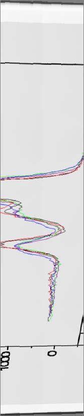
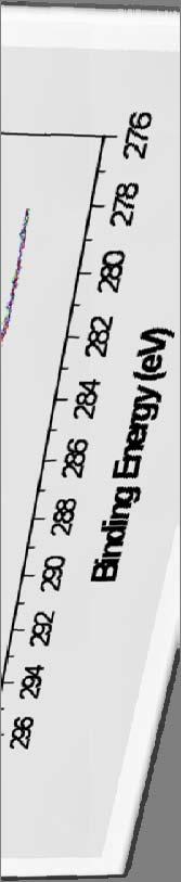
19 Atmospheric Plasma Surface Modification XPS spectrum results of untreated PTFE sample XPS spectrum results of treated PTFE sample


20 Atmospheric Plasma Surface Modification


21 Atmospheric Plasma Surface Modification Plasma Treatment Micro-Etching Effect Polyethylene (30,000 SEM magnification) Original Polymer Plasma-Treated
22 Roll-to-Roll PV Surface Cleaning Prior to Si Deposition Base Materials Lightweight, Flexible Will not shatter or be damaged during manufacture, handling, and subsequent operation in the field Thin stainless steel substrates, for example, have thermal time constant <10 ms - can be quickly heated and cooled to eliminate waiting for temperature stabilization Typically carry rolling oil deposits which must be removed Transport in deposition chambers is simple and reliable with little component wear, resulting in very low machine maintenance costs. Polymer Encapsulation Materials Polymer Encapsulation Materials Polymers such as EVA and Tefzel are flexible and lightweight Contaminated with residual organic polymer fragments, water, adsorbed gases
23 Roll-to-Roll PV Surface Cleaning Prior to Si Deposition Existing Base Material Wet Cleaning Roll material washed to produce clean, dry, particle-free substrate material suitable for Si deposition Web transported though detergent cleaning station, de-ionized water rinsing, IR drying Advantages of APT Cleaning/Functionalizing li i of Base, Encapsulation Films Base material contaminates volatilized/vaporized, increasing cleaning process efficiency. Encapsulant functionalization increases surface-to-reactive adhesive and surface-to-primer bond strength to flexible structures, and glass.
24 Crystalline Silicon (csi) PV Module Anti-reflective layer SiO2 layer Screen-printed Ag grid Pd layer Ti layer n-type silicon layer p-type silicon layer Metal/alloy back contact layer Atmospheric Plasma cleaning/functionalization Monolithic PV Module Glass / polymer encapsulation layer Atmospheric Plasma cleaning/functionalization PV cell layer Roll to roll fabricated backsheet layer with patterned circuitry i
25 Triple Junction Roll to Roll Amorphous Silicon (asi) PV Module Screen-printed Ag grid layer Anti-reflective ITO layer p-type layer a-si alloy layer n-type layer p-type layer a-sige alloy layer p-type layer a-sige alloy layer n-type silicon layer Silver & ZnO layer Metal/alloy back contact layer Atmospheric Plasma cleaning/functionalization Roll to Roll R llorganic PV Module Transparent top package / coating Transparent electrode Printed active material Primary electrode Metallized Polymer Film


26 APT Prescriptions for Flexible PV - Base 140 Minimum APT Power Density - Base W/m2/min Min. Power Density Stainless/Copper Alloy Copper/Nickel Alloy Stainless Steel Note: Inert/Reactive gas proportions influence minimum power densities.


27 APT Prescriptions for Flexible PV Thin Films 30 Minimum Power Density Thin Films W/ft2/min Minimum Power Density BOPET BOPVF ECTFE EPDM ETFE EVA PET PVF THV Note: Inert/Reactive gas proportions influence minimum power densities.
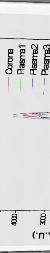
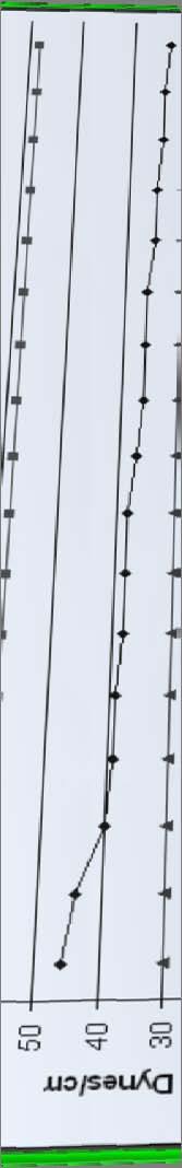
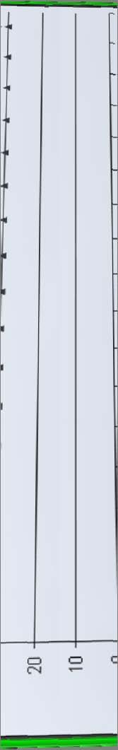
28 APT Prescriptions for Flexible PV Thin Films Substrate Corona Corona Plasma Plasma Watt Surface Watt Surface Density Tension Density Tension (W/ft 2 /min.) (Dynes/cm) (W/ft 2 /min.) (Dynes/cm) Polyimide PLA Tyvek


29 APT Prescriptions for Flexible PV Thin Films


 C. WD = 1.")
 D. WD = 2.")
30 APT Prescriptions for Flexible PV Corona Issues 2x2 micron images of PET film Topographical Image Phase Image (Height 10nm) (Range 60º) A. No Treatment B. WD = 1.16W/ft 2 /min (12.5W/m 2 /min) C. WD = 1.93W/ft 2 /min (20.8W/m 2 /min) D. WD = 2.71W/ft 2 /min (29.2W/m 2 /min)
31 APT Prescriptions for Flexible PV Emissions Wet Vs. Dry Metal/Metal Alloy Cleaning Metal Cleaning Process Chemical Wet Cleaning Atmospheric Plasma Dry Cleaning Active Cleaning Agent(s) Water-base Sulphuric Acid Ion/Electron/Photon Bombardment Alkaline Solutions Inert + Oxygen Gas Alcohol Solutions Detergent Solutions Dissolved within Chemical Agent(s) Rolling Oils Metal Oxides Water-Soluble Metal Derivatives n/a Entrained in Process Exhaust n/a Volatilized hydrocarbon particles Aluminum oxide particles Water-Soluble Aluminum Derivatives Emissions Water Laden w/ Chemical Wastes 15 ppm Ozone 2,336 ppm Inert gas (98%) 185 ppm Reactive O2 (70%) <10 ppm CO2 <10 ppm Water Vapor Volatized surface particulates Recurring Process Costs Fresh Water, Additional Chemicals Process Gases Handling, Disposal Costs
32 Conclusions Vacuum Plasma Surface Modification Anti-reflection Surface passivation Surface etching Layer deposition Process Evolutions Increasing chemical waste disposal issues Module per unit process cost reductions Thin Film PV Cell Fabrication CAGR expected to be 74.8% to 2015.
33 Conclusions Atmospheric (Dry) Plasma surface modification parameters (power density, gas chemistry) established for all flexible module components. Suitable for rigid module component surface preparation, such as frame and junction box sealing. In-line, continuous process No surface morphology effects Green technology, with no hazardous byproducts
34 Thank you for attending Reducing Solar Module Cost with Atmospheric Plasma Surface Modification Rory A. Wolf, Enercon Industries
Amorphous Silicon Solar Cells
 The Birnie Group solar class and website were created with much-appreciated support from the NSF CRCD Program under grants 0203504 and 0509886. Continuing Support from the McLaren Endowment is also greatly
Comparison of Atmospheric Plasma and Corona Treatments in Promoting Seal Strength
 Comparison of Atmospheric Plasma and Corona Treatments in Promoting Seal Strength Presented by Rory Wolf Business Unit Manager ITW Pillar Technologies Discussion Agenda o Study Objective o Extrusion Coating
Rory A. Wolf, Enercon Industries Corporation Amelia Sparavigna, Dipartimento di Fisica, Politecnico di Torino
 MODIFYING SURFACE FEATURES Extrusion Coating and Lamination Rory A. Wolf, Enercon Industries Corporation Amelia Sparavigna, Dipartimento di Fisica, Politecnico di Torino Abstract Extrusion coating, lamination
Metallization deposition and etching. Material mainly taken from Campbell, UCCS
 Metallization deposition and etching Material mainly taken from Campbell, UCCS Application Metallization is back-end processing Metals used are aluminum and copper Mainly involves deposition and etching,
Effects of Atmospheric Pressure Plasma on Adhesion
 Effects of Atmospheric Pressure Plasma on Adhesion Josh Sherwood, Loctite Industrial Adhesives, Henkel Corporation Presented at ANTEC - May, 2010 Abstract: Like any manufacturer, adhesive customers are
Ultra High Barrier Coatings by PECVD
 Society of Vacuum Coaters 2014 Technical Conference Presentation Ultra High Barrier Coatings by PECVD John Madocks & Phong Ngo, General Plasma Inc., 546 E. 25 th Street, Tucson, Arizona, USA Abstract Silicon
Roll-to-roll Technology for Transparent High Barrier Films
 Roll-to-roll Technology for Transparent High Barrier Films Presented at the AIMCAL Fall Technical Conference, October 19-22, 2008, Myrtle Beach, SC, USA Nicolas Schiller, John Fahlteich, Matthias Fahland,
EQUIPMENT AND SYSTEM FOR VACUUM COATING METALLIZING, SPUTTERING, PLASMA and PECVD. Hybrid system KOLZER DGK 36
 email : carlo.gennari@fastwebnet.it web site : http://carlogennariforni.beepworld.it/kolzer.htm EQUIPMENT AND SYSTEM FOR VACUUM COATING METALLIZING, SPUTTERING, PLASMA and PECVD Hybrid system KOLZER DGK
High Rate Deposition of Reactive Oxide Coatings by New Plasma Enhanced Chemical Vapor Deposition Source Technology
 General Plasma, Inc. 546 East 25th Street Tucson, Arizona 85713 tel. 520-882-5100 fax. 520-882-5165 High Rate Deposition of Reactive Oxide Coatings by New Plasma Enhanced Chemical Vapor Deposition Source
Fabrication Technology
 Fabrication Technology By B.G.Balagangadhar Department of Electronics and Communication Ghousia College of Engineering, Ramanagaram 1 OUTLINE Introduction Why Silicon The purity of Silicon Czochralski
Thin. Smooth. Diamond.
 UNCD Wafers Thin. Smooth. Diamond. UNCD Wafers - A Family of Diamond Material UNCD is Advanced Diamond Technologies (ADT) brand name for a family of thin fi lm diamond products. UNCD Aqua The Aqua series
X-ray Photoelectron Spectroscopy
 X-ray Photoelectron Spectroscopy X-ray photoelectron spectroscopy (XPS) is a non-destructive technique used to analyze the elemental compositions, chemical and electronic states of materials. XPS has a
Fabrication Techniques for Thin-Film Silicon Layer Transfer
 Fabrication Techniques for Thin-Film Silicon Layer Transfer S. L. Holl a, C. A. Colinge b, S. Song b, R. Varasala b, K. Hobart c, F. Kub c a Department of Mechanical Engineering, b Department of Electrical
MVTR Barrier of Metallized PLA Films
 MVTR Barrier of Metallized PLA Films Sigma Technologies Int l A. Yializis PhD Presented By: Steven Yializis 1 What Is PLA PLA is a Natural Product Based on Plant Photosynthesis H 2 O + CO 2 + Light CH
CYRANNUS. Welcome at iplas. See the latest developments! CYRANNUS.
 Welcome at iplas. See the latest developments! High performance plasma CYlindrical Resonator with ANNUlar Slots EH-tuner from vacuum to atmosphere uniform plasma large plasma extension high power density
Alternative Methods of Yttria Deposition For Semiconductor Applications. Rajan Bamola Paul Robinson
 Alternative Methods of Yttria Deposition For Semiconductor Applications Rajan Bamola Paul Robinson Origin of Productivity Losses in Etch Process Aggressive corrosive/erosive plasma used for etch Corrosion/erosion
Surface Micromachining
 Surface Micromachining Outline Introduction Material often used in surface micromachining Material selection criteria in surface micromachining Case study: Fabrication of electrostatic motor Major issues
Chapter 3 Silicon Device Fabrication Technology
 Chapter 3 Silicon Device Fabrication Technology Over 10 15 transistors (or 100,000 for every person in the world) are manufactured every year. VLSI (Very Large Scale Integration) ULSI (Ultra Large Scale
Production of PV cells
 Production of PV cells MWp 1400 1200 Average market growth 1981-2003: 32% 2004: 67% 1000 800 600 400 200 0 1991 1992 1993 1994 1995 1996 1997 1998 1999 2000 2001 2002 2003 2004 rest 1.0 1.0 1.0 2.0 4.0
Lecture Day 2 Deposition
 Deposition Lecture Day 2 Deposition PVD - Physical Vapor Deposition E-beam Evaporation Thermal Evaporation (wire feed vs boat) Sputtering CVD - Chemical Vapor Deposition PECVD LPCVD MVD ALD MBE Plating
Applied Research for Vacuum Web Coating: What is Coming Next?
 Applied Research for Vacuum Web Coating: What is Coming Next? Matthias Fahland, John Fahlteich, Steffen Günther, Manuela Junghähnel, Claus Luber, Nicolas Schiller, Cindy Steiner, Steffen Straach, Michiel
FLAIR. Air Flame Treatment. Enhanced Oxidation Corona
 FLAIR Air Flame Treatment Enhanced Oxidation Corona Plasmawerk Hamburg GmbH builds machinery for atmospheric pressure plasma treatment of fast moving, wide webs Plasmawerk Established, 2009 Largest order
Surface Modification: How low-pressure plasma treatments can benefit your manufacturing process
 Surface Modification: How low-pressure plasma treatments can benefit your manufacturing process surface modification Surface modification is growing exponentially as industrial engineers and manufacturers
UTILIZATION OF ATMOSPHERIC PLASMA SURFACE PREPARATION TO IMPROVE COPPER PLATING PROCESSES.
 SESSION 14 MATERIALS AND PROCESSES FOR ADVANCED PACKAGING UTILIZATION OF ATMOSPHERIC PLASMA SURFACE PREPARATION TO IMPROVE COPPER PLATING PROCESSES. Eric Schulte 1, Gilbert Lecarpentier 2 SETNA Corporation
LOW TEMPERATURE PHOTONIC SINTERING FOR PRINTED ELECTRONICS. Dr. Saad Ahmed XENON Corporation November 19, 2015
 LOW TEMPERATURE PHOTONIC SINTERING FOR PRINTED ELECTRONICS Dr. Saad Ahmed XENON Corporation November 19, 2015 Topics Introduction to Pulsed Light Photonic sintering for Printed Electronics R&D Tools for
Procese de depunere in sistemul Plasma Enhanced Chemical Vapor Deposition (PECVD)
") Procese de depunere in sistemul Plasma Enhanced Chemical Vapor Deposition (PECVD) Ciprian Iliescu Conţinutul acestui material nu reprezintă in mod obligatoriu poziţia oficială a Uniunii Europene sau a
Procese de depunere in sistemul Plasma Enhanced Chemical Vapor Deposition (PECVD) Ciprian Iliescu Conţinutul acestui material nu reprezintă in mod obligatoriu poziţia oficială a Uniunii Europene sau a
ITO SPUTTER COATED FILMS FOR TOUCH PANEL APPLICATIONS USING ROTARY SINTERED CERAMIC ITO TARGETS: WHAT CAN BE LEARNED FROM GLASS COATING?
 ITO SPUTTER COATED FILMS FOR TOUCH PANEL APPLICATIONS USING ROTARY SINTERED CERAMIC ITO TARGETS: WHAT CAN BE LEARNED FROM GLASS COATING? Paul Lippens AIMCAL Web coating conference 2012 Outline Introduction
A discussion of crystal growth, lithography, etching, doping, and device structures is presented in
 Chapter 5 PROCESSING OF DEVICES A discussion of crystal growth, lithography, etching, doping, and device structures is presented in the following overview gures. SEMICONDUCTOR DEVICE PROCESSING: AN OVERVIEW
Atomic Layer Deposition(ALD)
") Atomic Layer Deposition(ALD) AlO x for diffusion barriers OLED displays http://en.wikipedia.org/wiki/atomic_layer_deposition#/media/file:ald_schematics.jpg Lam s market-leading ALTUS systems combine CVD
Atomic Layer Deposition(ALD) AlO x for diffusion barriers OLED displays http://en.wikipedia.org/wiki/atomic_layer_deposition#/media/file:ald_schematics.jpg Lam s market-leading ALTUS systems combine CVD
A Technology Decision Adhesive Lamination or Extrusion Coating/Lamination?
 A Technology Decision Adhesive Lamination or Extrusion Coating/Lamination? Rory Wolf, Enercon Industries Corporation Abstract Extrusion-based coating/laminating and adhesive-based film laminating are different
CSI G SYSTEMS CSI GAS DELIVERY SUPPORT. Chemical Vapor Deposition (CVD)
") This page discusses the CVD processes often used for integrated circuits (ICs). Particular materials are deposited best under particular conditions. Facilitation recommendations are at the bottom of the
This page discusses the CVD processes often used for integrated circuits (ICs). Particular materials are deposited best under particular conditions. Facilitation recommendations are at the bottom of the
Plasma for Underfill Process in Flip Chip Packaging
 Plasma for Underfill Process in Flip Chip Packaging Jack Zhao and James D. Getty Nordson MARCH 2470-A Bates Avenue Concord, California 94520-1294 USA Published by Nordson MARCH www.nordsonmarch.com 2015
Adhesion in Extrusion Coating & Laminating - the Importance of Machine Variables. Bruce Foster Mica Corporation
 Adhesion in Extrusion Coating & Laminating - the Importance of Machine Variables Bruce Foster Mica Corporation Outline Identify key factors that affect adhesion Examine Machine Variables that affect these
Turn-key Production System for Solar Cells
 SOLARE Turn-key Production System for Solar Cells 02 Innovations for New Technologies provides technology solutions for both crystalline and thin-film highperformance solar cell platforms. Our production
EECS130 Integrated Circuit Devices
 EECS130 Integrated Circuit Devices Professor Ali Javey 9/13/2007 Fabrication Technology Lecture 1 Silicon Device Fabrication Technology Over 10 15 transistors (or 100,000 for every person in the world)
ELEC 3908, Physical Electronics, Lecture 4. Basic Integrated Circuit Processing
 ELEC 3908, Physical Electronics, Lecture 4 Basic Integrated Circuit Processing Lecture Outline Details of the physical structure of devices will be very important in developing models for electrical behavior
From Vacuum to Atmosphere and back an in-house Process Chain for Different Products
 From Vacuum to Atmosphere and back an in-house Process Chain for Different Products Dr. Steffen Günther Vacuum coating low pressure 10-1 10-4 Pa (10-3 10-6 mbar) unhindered particle movement no unintended
Transactions on Engineering Sciences vol 2, 1993 WIT Press, ISSN
 A study of thin-film continuous coating process by vapour deposition P. Gimondo," F. Arezzo,* B. Grifoni,* G. Jasch& "Centra Sviluppo Materiali SpA, Via di Castel & Von Ardenne Anlagentchnik GmbH, Plattleite
Energy Efficient Glazing Design. John Ridealgh Off-Line Coatings Technology Group Pilkington European Technology Centre
 Energy Efficient Glazing Design John Ridealgh Off-Line Coatings Technology Group Pilkington European Technology Centre 2 John Ridealgh 30th November 2009 Talk Outline Pilkington Group Limited & NSG Group
TECHNOLOGY PLASMA. Ahornweg Weikersheim, Germany
 TECHNOLOGY TECHNOLOGY The plasma process is used to optimally prepare material surfaces before processes such as gluing, soldering, bonding, wire-bonding, injection molding, potting, coating, printing
Etching Mask Properties of Diamond-Like Carbon Films
 N. New Nawachi Diamond et al. and Frontier Carbon Technology 13 Vol. 15, No. 1 2005 MYU Tokyo NDFCT 470 Etching Mask Properties of Diamond-Like Carbon Films Norio Nawachi *, Akira Yamamoto, Takahiro Tsutsumoto
Linear Plasma Sources for Surface Modification and Deposition for Large Area Coating
 Linear Plasma Sources for Surface Modification and Deposition for Large Area Coating Dr Tony Williams Gencoa Ltd, UK Victor Bellido-Gonzalez, Dr Dermot Monaghan, Dr Joseph Brindley, Robert Brown SVC 2016,
Solar Cells Fabrication Technologies
 Solar Cells Fabrication Technologies Crystalline Si Cell Technologies Amorphous Si Cell Technologies Thin Film Cell Technologies For a comprehensive tutorial on solar cells in general, see www.udel.edu/igert/pvcdrom
Temperature Scales. Questions. Temperature Conversions 7/21/2010. EE580 Solar Cells Todd J. Kaiser. Thermally Activated Processes
 7/1/010 EE80 Solar Cells Todd J. Kaiser Flow of Wafer in Fabrication Lecture 0 Microfabrication A combination of Applied Chemistry, Physics and ptics Thermal Processes Diffusion & xidation Photolithograpy
A Deep Silicon RIE Primer Bosch Etching of Deep Structures in Silicon
 A Deep Silicon RIE Primer Bosch Etching of Deep Structures in Silicon April 2009 A Deep Silicon RIE Primer 1.0) Etching: Silicon does not naturally etch anisotropically in fluorine based chemistries. Si
IMRE/ETPL Flagship Project
 IMRE/ETPL Flagship Project Nanoparticulate Barrier Films & Gas Permeation Measurement Techniques for Thin Film Solar & Display Application Problems Senthil Ramadas Institute of Materials Research & Engineering
Thin film silicon technology. Cosimo Gerardi 3SUN R&D Tech. Coordinator
 Thin film silicon technology Cosimo Gerardi 3SUN R&D Tech. Coordinator 1 Outline Why thin film Si? Advantages of Si thin film Si thin film vs. other thin film Hydrogenated amorphous silicon Energy gap
Deposition Technology and Applications of DLC Films
 TECHNICAL REPORT Deposition Technology and Applications of DLC Films M. SUZUKI K. YAMAKAWA T. SAITO Diamond-Like Carbon (DLC) films possess good properties such as low friction, high wear resistance, high
Visit
 Practical Applications for Nano- Electronics by Vimal Gopee E-mail: Vimal.gopee@npl.co.uk 10/10/12 Your Delegate Webinar Control Panel Open and close your panel Full screen view Raise hand for Q&A at the
Mastering Corona Treaters, Roll Coverings, & Electrodes for Extrusion Film Lines
 Mastering Corona Treaters, Roll Coverings, & Electrodes for Extrusion Film Lines Today s presenters Aaron Hootkin Regional Sales Manager Tom Gilbertson VP Application Engineering Seminar Overview Surface
Thin Films: Sputtering Systems (Jaeger Ch 6 & Ruska Ch 7,) Can deposit any material on any substrate (in principal) Start with pumping down to high
 Can deposit any material on any substrate (in principal) Start with pumping down to high") Thin Films: Sputtering Systems (Jaeger Ch 6 & Ruska Ch 7,) Can deposit any material on any substrate (in principal) Start with pumping down to high vacuum ~10-7 torr Removes residual gases eg oxygen from
Thin Films: Sputtering Systems (Jaeger Ch 6 & Ruska Ch 7,) Can deposit any material on any substrate (in principal) Start with pumping down to high vacuum ~10-7 torr Removes residual gases eg oxygen from
TPOs in Automotive, 2002, ECM, June 17-19, 2002, Novi, Michigan / USA SURFACE TREATMENT OF SANTOPRENE FOR ADHESIVE BONDING
 SURFACE TREATMENT OF SANTOPRENE FOR ADHESIVE BONDING P. Hoobin, W.S. Gutowski, M. Morehouse Polymer Surface Engineering Group CSIRO Division of Building, Construction and Engineering Melbourne / Australia
LOT. Contents. Introduction to Thin Film Technology. Chair of Surface and Materials Technology
 Introduction to Thin Film Contents 1. Introduction and Application Examples (2h) 2. Preparation of Thin Films by PVD (Physical Vapor Deposition) (6h) 2.1 Vacuum Technique (1h) 2.1.1 Kinetics of Gases 2.1.2
Silicon Manufacturing
 Silicon Manufacturing Group Members Young Soon Song Nghia Nguyen Kei Wong Eyad Fanous Hanna Kim Steven Hsu th Fundamental Processing Steps 1.Silicon Manufacturing a) Czochralski method. b) Wafer Manufacturing
University of Minnesota Nano Center Standard Operating Procedure
 Equipment Name: University of Minnesota Nano Center PECVD Coral Name: pecvd Revision Number: 2.0 Model: Plasmatherm 340 Revisionist: Mark Fisher Location: Bay 3 Date: 20 Sept 2013 1 Description The Plasmatherm
Surface Preparation Challenges in Crystalline Silicon Photovoltaic Manufacturing
 Surface Preparation Challenges in Crystalline Silicon Photovoltaic Manufacturing Kristopher Davis 1,3, Andrew C. Rudack 2,3, Winston Schoenfeld 1,3 Hubert Seigneur 1,3, Joe Walters 1,3, Linda Wilson 2,3
Drytech Quad Etch Recipes Dr. Lynn Fuller Mike Aquilino Microelectronic Engineering
 ROCHESTER INSTITUTE OF TECHNOLOGY MICROELECTRONIC ENGINEERING Drytech Quad Etch Recipes Dr. Lynn Fuller Mike Aquilino 82 Lomb Memorial Drive Rochester, NY 14623-5604 Tel (585) 475-2035 Fax (585) 475-5041
Supporting Information
 Supporting Information Fast-Response, Sensitivitive and Low-Powered Chemosensors by Fusing Nanostructured Porous Thin Film and IDEs-Microheater Chip Zhengfei Dai,, Lei Xu,#,, Guotao Duan *,, Tie Li *,,
Explain, in terms of structure and bonding, why sodium oxide has a high melting point
 Q1.Some melting points of Period 3 oxides are given in this table. Na 2O SiO 2 SO 2 SO 3 Melting point / K 1548 1883 200 290 (a) Explain, in terms of structure and bonding, why sodium oxide has a high
Photolithography I ( Part 2 )
") 1 Photolithography I ( Part 2 ) Chapter 13 : Semiconductor Manufacturing Technology by M. Quirk & J. Serda Bjørn-Ove Fimland, Department of Electronics and Telecommunication, Norwegian University of Science
1 Photolithography I ( Part 2 ) Chapter 13 : Semiconductor Manufacturing Technology by M. Quirk & J. Serda Bjørn-Ove Fimland, Department of Electronics and Telecommunication, Norwegian University of Science
Grid-Tied PV System with Energy Optimization
 International Journal of Engineering Works Kambohwell Publisher Enterprises Vol. 4, Issue 10, PP. 184-189, October 2017 www.kwpublisher.com Grid-Tied PV System with Energy Optimization Maryam Shahjehan,
INTRODUCTION AND OVERVIEW OF MANUFACTURING. Manufacturing is Important. Manufacturing - Technologically Important
 INTRODUCTION AND OVERVIEW OF MANUFACTURING 1. What is Manufacturing? 2. Materials in Manufacturing 3. Manufacturing Processes 4. Production Systems 5. Organization of the Book Manufacturing is Important
Micro-Electro-Mechanical Systems (MEMS) Fabrication. Special Process Modules for MEMS. Principle of Sensing and Actuation
 Fabrication. Special Process Modules for MEMS. Principle of Sensing and Actuation") Micro-Electro-Mechanical Systems (MEMS) Fabrication Fabrication Considerations Stress-Strain, Thin-film Stress, Stiction Special Process Modules for MEMS Bonding, Cavity Sealing, Deep RIE, Spatial forming
Micro-Electro-Mechanical Systems (MEMS) Fabrication Fabrication Considerations Stress-Strain, Thin-film Stress, Stiction Special Process Modules for MEMS Bonding, Cavity Sealing, Deep RIE, Spatial forming
The most important parameters determining the performance of a cutting blade are:
 Diamond blades exceptionally wear resistant and extremely sharp P. Gluche 1, S. Strobel 1, H.-J. Fecht 2 1 GFD Gesellschaft für Diamantprodukte mbh, Lise-Meitner-Str. 13, 89081 Ulm, Germany 2 University
Semiconductor Manufacturing Technology. IC Fabrication Process Overview
 Semiconductor Manufacturing Technology Michael Quirk & Julian Serda October 00 by Prentice Hall Chapter 9 IC Fabrication Process Overview /4 Objectives After studying the material in this chapter, you
Technical Specification
 Technical Specification No.: Vacuum 005/2008 Version 1.6 / 22.09.2010 Guidelines for UHV-Components at DESY U. Hahn (FS-BT), K. Zapfe (MVS) Contents 1 General Information... 3 1.1 Introduction... 3 1.2
ABSTRACT: INTRODUCTION:
 ABSTRACT: Nano-Composite Polymer Optical Coatings Tom Faris Vampire Optical Coatings, Inc. P.O. Box 240 Kirkersville, Ohio 43033 (740)-927-5257 f(740)-927-5032 vampirecoatings@earthlink.net Traditionally
Silver Diffusion Bonding and Layer Transfer of Lithium Niobate to Silicon
 Chapter 5 Silver Diffusion Bonding and Layer Transfer of Lithium Niobate to Silicon 5.1 Introduction In this chapter, we discuss a method of metallic bonding between two deposited silver layers. A diffusion
Course schedule. Universität Karlsruhe (TH)
") Course schedule 1 Preliminary schedule 1. Introduction, The Sun 2. Semiconductor fundamentals 3. Solar cell working principles / pn-junction solar cell 4. Silicon solar cells 5. Copper-Indiumdiselenide
Course schedule 1 Preliminary schedule 1. Introduction, The Sun 2. Semiconductor fundamentals 3. Solar cell working principles / pn-junction solar cell 4. Silicon solar cells 5. Copper-Indiumdiselenide
Summer School June 2-4 th 2015
 MAT4BAT Advanced materials for batteries Summer School June 2-4 th 2015 «Electrode formulation and processing» Dane Sotta (CEA-Liten, France) Mat4Bat Summer School Dane Sotta (CEA) June 3 rd 2015 1 Outline
Adhesives for Bonding Polyurethane: A Process Review PTS Seminar Polyurethane Manufacturers Association. Outline
 Adhesives for Bonding Polyurethane: A Process Review PTS Seminar Polyurethane Manufacturers Association Jeff Means, Technical Service Representative LORD Corporation May 8, 2010 Outline Overview of the
KGC SCIENTIFIC Making of a Chip
 KGC SCIENTIFIC www.kgcscientific.com Making of a Chip FROM THE SAND TO THE PACKAGE, A DIAGRAM TO UNDERSTAND HOW CPU IS MADE? Sand CPU CHAIN ANALYSIS OF SEMICONDUCTOR Material for manufacturing process
Vacuum Plasma Deposition of Water and Oil Repellent Nano-coatings
 Vacuum Plasma Deposition of Water and Oil Repellent Nano-coatings AIMCAL Web Coating & Handling Conference 2014 Europe Dr Nicholas Rimmer P2i 127 Olympic Avenue, Milton Park, Abingdon, Oxfordshire, OX14
Anticorrosive Coatings
 Anticorrosive Coatings Joerg Sander 1 Introduction 1.1 Why corrosion-protective coatings 1.2 Literature 2 Corrosion protection coatings 2.1 Principles of function 2.1.1 Electrochemistry of corrosion inhibition
Using Argon Plasma to Remove Fluorine, Organic and Metal Oxide Contamination for Improved Wire Bonding Performance
 Using Argon Plasma to Remove Fluorine, Organic and Metal Oxide Contamination for Improved Wire Bonding Performance Scott D. Szymanski March Plasma Systems Concord, California, U.S.A. sszymanski@marchplasma.com
PPS Outshines Stainless Steel in Chemically-Hostile Valve Applications
 PPS Outshines Stainless Steel in Chemically-Hostile Valve Applications What is PPS? Polyphenylene Sulfide (PPS), is a high performance, fiber reinforced, advanced composite, linear thermoplastic polymer.
Optimization of Ion and Electron Properties in IC Packaging Applications
 Optimization of Ion and Electron Properties in IC Packaging Applications Plasma surface-treatment techniques can improve wire bonding and eliminate substrate delamination. Christa Fairfield Nordson MARCH
Improvement in the Adhesive Property of Chemically Stable Polymeric Materials and FRP
 THE 19 TH INTERNATIONAL CONFERENCE ON COMPOSITE MATERIALS Improvement in the Adhesive Property of Chemically Stable Polymeric Materials and FRP H. Kanazawa* and A. Inada Department of Industrial Systems,
1. Introduction. What is implantation? Advantages
 Ion implantation Contents 1. Introduction 2. Ion range 3. implantation profiles 4. ion channeling 5. ion implantation-induced damage 6. annealing behavior of the damage 7. process consideration 8. comparison
REDUCTION OF REFLECTION LOSSES IN SOLAR CELL BY USING TIAL2 AND ZR ANTI REFLECTIVE COATING
 IJRET: International Journal of Research in Engineering and Technology eissn: 2319-1163 pissn: 2321-738 REDUCTION OF REFLECTION LOSSES IN SOLAR CELL BY USING TIAL2 AND ZR ANTI REFLECTIVE COATING S. Anandhi
END-OF-LIFE PATHWAYS FOR PHOTOVOLTAIC BACKSHEETS
 FINAL REPORT END-OF-LIFE PATHWAYS FOR PHOTOVOLTAIC BACKSHEETS Presented by: Fraunhofer Institute for Environmental, Safety and Energy Technology UMSICHT Director Prof. Eckhard Weidner Osterfelder Strasse
Visualization and Control of Particulate Contamination Phenomena in a Plasma Enhanced CVD Reactor
 Visualization and Control of Particulate Contamination Phenomena in a Plasma Enhanced CVD Reactor Manabu Shimada, 1 Kikuo Okuyama, 1 Yutaka Hayashi, 1 Heru Setyawan, 2 and Nobuki Kashihara 2 1 Department
SolarWindow. Innovating Alternative and Renewable Energy Solutions. Corporate» Technology» Media» Investors» Contact
 Innovating Alternative and Renewable Energy Solutions A A A Corporate» Technology» Media» Investors» Contact SolarWindow New Energy Technologies is developing the first-of-its kind SolarWindow technology,
Freshure Coatings: Environmentally Friendly Barrier Coatings
 Freshure Coatings: Environmentally Friendly Barrier Coatings Shahab Jahromi Knowfort Technologies BV Urmonderbaan 20a 6160MD Geleen The Netherlands Email: s.jahromi@knowfort.com Introduction. Roll-to-roll
MATERIALS OF CONSTRUCTION
 HIGH PRESSURE PURIFIER (MODEL SG6140) Model SG6140 purifier is designed to remove water and/or oil from gas or liquid streams. In the laboratory, it protects delicate or sensitive instruments, prolongs
Yung-Hui Yeh, and Bo-Cheng Kung Display Technology Center (DTC), Industrial Technology Research Institute, Hsinchu 310, Taiwan
, Industrial Technology Research Institute, Hsinchu 310, Taiwan") Amorphous In 2 O 3 -Ga 2 O 3 -ZnO Thin Film Transistors and Integrated Circuits on Flexible and Colorless Polyimide Substrates Hsing-Hung Hsieh, and Chung-Chih Wu* Graduate Institute of Electronics Engineering,
Amorphous In 2 O 3 -Ga 2 O 3 -ZnO Thin Film Transistors and Integrated Circuits on Flexible and Colorless Polyimide Substrates Hsing-Hung Hsieh, and Chung-Chih Wu* Graduate Institute of Electronics Engineering,
Atmospheric plasma technology for surface modification of nanoparticles
 9/16/2011 Atmospheric plasma technology for surface modification of nanoparticles Dirk Vangeneugden - COST Meeting, Espoo, Finland, 15-16/09/2011 Contents Introduction to VITO Developed atmospheric plasma
There are basically two approaches for bulk micromachining of. silicon, wet and dry. Wet bulk micromachining is usually carried out
 57 Chapter 3 Fabrication of Accelerometer 3.1 Introduction There are basically two approaches for bulk micromachining of silicon, wet and dry. Wet bulk micromachining is usually carried out using anisotropic
Plasma-Enhanced Chemical Vapor Deposition
 Plasma-Enhanced Chemical Vapor Deposition Steven Glenn July 8, 2009 Thin Films Lab 4 ABSTRACT The objective of this lab was to explore lab and the Applied Materials P5000 from a different point of view.
micro resist technology
 Characteristics Processing guidelines Negative Tone Photoresist Series ma-n 1400 ma-n 1400 is a negative tone photoresist series designed for the use in microelectronics and microsystems. The resists are
FABRICATION ENGINEERING MICRO- NANOSCALE ATTHE AND. Fourth Edition STEPHEN A. CAMPBELL. of Minnesota. University OXFORD UNIVERSITY PRESS
 AND FABRICATION ENGINEERING ATTHE MICRO- NANOSCALE Fourth Edition STEPHEN A. CAMPBELL University of Minnesota New York Oxford OXFORD UNIVERSITY PRESS CONTENTS Preface xiii prrt i OVERVIEW AND MATERIALS
Plasma Etching Rates & Gases Gas ratios affects etch rate & etch ratios to resist/substrate
 Plasma Etching Rates & Gases Gas ratios affects etch rate & etch ratios to resist/substrate Development of Sidewalls Passivating Films Sidewalls get inert species deposited on them with plasma etch Creates
Recent Advances in Atmospheric Plasma Treatment of Textiles. Gregory Roche, Carrie Cornelius, Wade Tyner ApJet, Inc.
 Recent Advances in Atmospheric Plasma Treatment of Textiles, Carrie Cornelius, Wade Tyner ApJet, Inc. Abstract Atmospheric pressure plasma is a revolutionary new technology for surface finishing and pretreatments.
Printed Electronics: Photonic Curing and Enabled Materials
 Printed Electronics: Photonic Curing and Enabled Materials Kurt Schroder, Dave Pope, Ian Rawson NovaCentrix 200-B Parker Dr Suite 580 Austin, TX 78728 Extended Abstract Introduction Photonic curing is
Meeting the Demands of Renewable Energy:
 Capture & Storage Advanced Batteries Meeting the Dems of Renewable Energy: Lithium Cathodes: CXFE030 SID4220.5 CXLI083 Cathode Fabrication O r ganosil i c o n Solid Polymer, Gel Electrolyte Systems, Li-SPE
Materials Characterization
 Materials Characterization C. R. Abernathy, B. Gila, K. Jones Cathodoluminescence (CL) system FEI Nova NanoSEM (FEG source) with: EDAX Apollo silicon drift detector (TE cooled) Gatan MonoCL3+ FEI SEM arrived
Water Vapor and Carbon Nanotubes
 Water Vapor and Carbon Nanotubes Published technical papers on carbon nanotube fabrication point out the need to improve the growth rate and uniformity of Carbon Nanotubes. CNT faces major hurdles in its
Reactor wall plasma cleaning processes after InP etching in Cl 2 /CH 4 /Ar ICP discharge
 Reactor wall plasma cleaning processes after InP etching in Cl 2 /CH 4 /Ar ICP discharge R. Chanson a, E. Pargon a, M. Darnon a, C. Petit Etienne a, S. David a, M. Fouchier a, B. Glueck b, P. Brianceau
Recap of a-si and a-si cell technology Types of a-si manufacturing systems a-si cell and module manufacturing at Xunlight. Xunlight Corporation
 Thin-Film Silicon Technology and Manufacturing Recap of a-si and a-si cell technology Types of a-si manufacturing systems a-si cell and module manufacturing at Xunlight Xunlight products and installations
Synthesis and Characterization of Zinc Iron Sulphide (ZnFeS) Of Varying Zinc Ion Concentration
 Of Varying Zinc Ion Concentration") International Journal of Science and Technology Volume 5 No. 5, May, 2016 Synthesis and Characterization of Zinc Iron Sulphide (ZnFeS) Of Varying Zinc Ion Concentration I. B. Obasi 1 and J. C. Osuwa 2
International Journal of Science and Technology Volume 5 No. 5, May, 2016 Synthesis and Characterization of Zinc Iron Sulphide (ZnFeS) Of Varying Zinc Ion Concentration I. B. Obasi 1 and J. C. Osuwa 2