SUSS SOLUTIONS FOR LARGE FORMAT PATTERNING UV Scanning Lithography and Excimer Laser Ablation
|
|
|
- Linda Nancy Townsend
- 6 years ago
- Views:
Transcription


1 SUSS SOLUTIONS FOR LARGE FORMAT PATTERNING UV Scanning Lithography and Excimer Laser Ablation Kevin Yang, Habib Hichri, Ralph Zoberbier SÜSS MicroTec Photonic Systems Inc. June 18, 2015

2 MARKET DRIVER Mobile Applications drive Advanced Packaging Development. Small Form Factor High Performance High Bandwidth Low Power Consumption Low Cost Smaller L/S and Via Higher I/O count Higher Yield Higher Reliability + Higher Performance + Lower Cost 2

3 AP PLATFORMS AND PROCESS STEPS s patterning solution: UV Scanner and Excimer Laser Ablation System 3


4 AP INFRASTRUCTURE ROADMAP All platforms may coexist. 450mm being slow, panel based packaging will grow. Each sector has different benefits. OSAT, IDM: FOWLP Substrate Manufacturer: Embedded Die Same requirements: Cost, Size, Performance Collaboration required for reliable infrastructure Yole Developpement


5 LARGE PANEL ADVANTAGES Wafer vs. Panel: technology dependent Rectangular: natural choice for better fit and surface utilization Throughput: reduced handling/transfer time Standards and Infrastructure Process and equipment Size Material 5
6 PHOTOLITHOGRAPHY VS. DIRECT ABLATION Photolithography Proven technology Resolution limitation Multistep process Hazardous/environmentally unfriendly wet chemical process Balance of the photo characteristics with the desired thermal/mechanical properties of the material Cure of the polymer after photo-process Excimer Laser Ablation Direct material removal according to the mask pattern Simpler process without wet develop step Fine via with high aspect ratio Material properties not limited by the need of photo-imaging Cure of the polymer before laser processing 6


 DSC500 /")

7 SUSS EXPOSURE PRODUCT PORTFOLIO Mask Aligner Projection Scanner Excimer Ablation System MA200 Gen3 Automatic 150/200mm MA300 Gen2 Automatic 200/300mm DSC300 Gen2 Automatic 200/300mm ELP300 Gen2 Automatic 200/300mm MA/BA8 Gen3 Semi-Automatic Pieces up to 200mm MA12 Manual 200/300mm (squares) DSC500 / DSC800 Automatic 450x500mm / 650x780mm ELP600 Automatic 600x600mm 7


8 DSC300/500/800 UV PROJECTION SCANNER Proven UV projection scanning technology Low cost Full-Field No-Stitch 1:1 Projection Imaging Alignment accuracy: TSA < 1µm Variable NA high DoF to high resolution Full automation Wafers: 200mm, 300mm, 450mm Panels: 450x500mm, 650 x 780mm DSC Wafers DSC500: Near Vertical Orientation DSC300 Beam Delivery System DSC500 - Panels 8


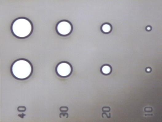
9 DSC PROJECTION SCANNER IMAGING EXAMPLES 30µm vias in 100µm WBR µm vias in 80µm AZ125nXT 5µm vias in 10µm AZ10XT 6µm and 7µm L/S in 15µm AZ4620 6µm vias in 10µm HD8820 PBO 10µm L/S in 12µm AZ15nxT 9

10 ELP 300/600 EXIMER ABLATION SYSTEM ELP300: up to 300mm wafer ELP600: up to 600mm x 600mm substrate ELP300 ELP600 10

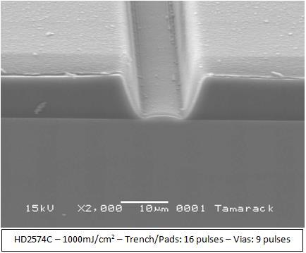
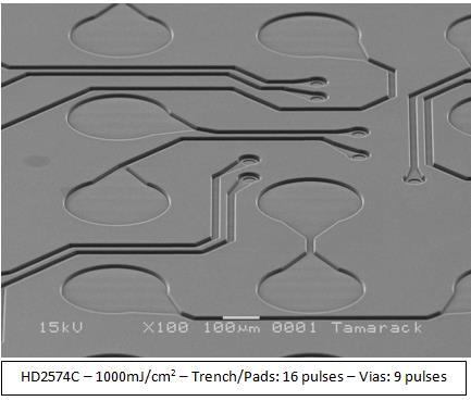
11 EXCIMER LASER ABLATION 248nm and 308nm Direct removal of the material Add enough energy to break the molecular bonds at the surface. Limited thermal effect for heating or change to adjacent area or underlying material. Mask based projection Throughput independent of the pattern shape or density. Suitable Materials: Most organic materials Polymers/Organic Dielectrics (PI, PBO, BCB, Epoxy etc.) Epoxy Mold Compounds (EMC filled and unfilled) Some inorganics Dielectrics (SiNx < 1µm thick with 248nm ) Thin metals (Ti, TiW, TaN, Ta, Cu, Ag, Al, etc. < 600nm thick on organic material) Conductive materials (ITO, IZO, CNT < 1µm thick on organic material) mask substrate 11
 can be predicted.")


12 EXCIMER LASER ABLATION Fluence and Etch Rate With threshold fluence F 0 ~ constant etch depth per pulse (etch rate) can be predicted. Depth control by number of pulses Metal Pad as Etch Stop Metal pads (> ~1µm) become natural stop layer for Excimer via ablation. Flexibility for material thickness variation. Via 30µm Stopped on Cu pad No etching of Cu Cu Pad Al Pad Y. H. Chen, H. Y. Zheng, K. S. Wong, and S. C. Tam, Excimer laser drilling of polymers, Proc. SPIE 3184,
13 Etch Depth (μm) Ablation rate, µm/pulse Etch Rate (μm) WAVELENGTH, FLUENCE, PULSE, AND ETCH RATE Absorption and etch rate vary: Wavelength Fluence Etch depth control by number of pulses 0.6 Polyimide Ablation Rate Dependence on Wavelength KrF 248 nm XeCl 308 nm Linear (XeCl 308 nm) Number of Pulses Fluence Fluence, mj/cm² (mj/cm 2 ) 13

14 SIDE-WALL ANGLE AND FLUENCE Side-wall Angle controlled by Fluence Steeper wall with higher fluence Higher etch rate with higher fluence mj/cm 2, 45 pulses 1200 mj/cm 2, 12 pulses 14

15 EXCIMER LASER ABLATION ADVANTAGES Technical benefits Higher via resolution < 3μm (2μm demonstrated) High overlay control: 300mm Wafer: +/- 1μm Panels: +/- 2μm Side-wall angle control Limited thermal effect Simpler process Eliminate develop and chemical etch steps Reduce bake/curing step Safety and environmental protection Reduction of hazardous process steps and chemicals Reduction of chemical waste Benefit with Non-Photo Material Cost Reduction Combination of desirable material properties 15
16 PHOTO AND NON-PHOTO MATERIAL EXAMPLE Non-photo material s advantages Desirable properties Low cost Photo/Non-Photo Non-Photo Photo Material PI PI Manufacturer HD Micro HD Micro Product PI-2611 HD-4100 CTE (ppm/ C) 3 35 Modulus (GPa) Tensile Strength (MPa) Elongation (%)

17 ELP600 TECHNICAL CHARACTERISTICS ELP600 17


 JSR")


18 ELP EXCIMER STEPPER PATTERNING EXAMPLES (PHOTO MATERIAL) JSR WPR µm HD8930 PBO 13µm HD µm 40 µm vias 15 µm dia vias 18


19 ELP EXCIMER STEPPER PATTERNING EXAMPLES (NON-PHOTO MATERIAL) EMC (undisclosed) 10µm HD (proprietary) 8µm Dow BCB Cyclotene 302X 12µm HD


20 ELP EXCIMER STEPPER PATTERNING EXAMPLES (BCB CROSS SECTION) Mask: 7 μm Top: 6 μm Bottom: 4.2 μm 650 mj/cm 2 Mask: 5 μm Top: 4.1 μm Bottom: 2.6 μm 650 mj/cm 2 Michael Töpper, Karin Hauck, Mario Schima Danny Jaeger, Klaus- Dieter Lang, A sub-4 μm Via Technology of Thin film Polymers using Scanning Laser Ablation, ECTC


21 ELP EXCIMER STEPPER PATTERNING EXAMPLES (BCB DRY FILM CROSS SECTION) Mask: 10 μm Top: 10.3 μm Bottom: 7.2 μm Thickness: 15 μm Mask: 5 μm Top: 4.7 μm Bottom: 2.8 μm Thickness: 15 μm Michael Töpper, Karin Hauck, Mario Schima Danny Jaeger, Klaus- Dieter Lang, A sub-4 μm Via Technology of Thin film Polymers using Scanning Laser Ablation, ECTC


22 ELP EXCIMER STEPPER PATTERNING EXAMPLES (FILLED VIA AND RDL) polishing mold 40µm 2 metal layer with 10µm fully filled micro-vias 10µm at 40µm pitch and 2.5µm line 10µm ZS100 30µm: buffer layer (ZS100) Glass (300µm: core) 8-10µm fully filled micro-vias at 20µm pitch Yuya Suzuki, Jan Brune, Rolf Senczuk, Rainer Pätzel, Ryuta Furuya, Fuhan Liu, Venky Sundaram, Rao Tummala, Demonstration of 20μm Pitch Micro-vias by Excimer Laser Ablation in Ultra-thin Dry-film Polymer Dielectrics for Multilayer RDL on Glass Interposers, ECTC 2015 Georgia Tech PRC ZEON 22


23 POST LASER ABLATION CLEANING Post ablation cleaning is required for subsequent processes in most cases. before after Sacrificial layer Successful cleaning of HD4104 Sacrifiall layer removed with high-pressure CO 2 ionized water Sacrificial Layer O 2 plasma cleaning Successful cleaning of PBO, BCB, HD2611, HD4110 In-house tool (vacuum plasma) available CO 2 snow cleaning Successful cleaning PBO with most aggressive CO 2 snow 3rd party tool available O 2 plasma DPSS Cleaning Successful cleaning PBO (HD8820) Using pico second DPSS Laser In-house tool available CO 2 snow The material determines the cleaning method. DPSS 23
24 SUMMARY Mobile products drive packaging trend Cost, Form Factor, Performance, Yield Large size rectangular panel will grow for high volume manufacturing. Driven by cost reduction Patterning is a major factor along with material development. Suss MicroTec provides Mask Aligner, UV Projection Scanner and Excimer Laser Ablation for patterning applications. UV scanner and excimer laser stepper are available for large format patterning. Excimer laser stepper provides maximum benefits with non-photo materials. Excimer laser stepper applications in RDL Via and Trench formation, SLR and Laser Debonding. Demo and evaluation test available In-house at Suss MicroTec Fraunhofer Institute IZM ELP600 24
25 25
FABRICATION AND RELIABILITY OF ULTRA-FINE RDL STRUCTURES IN ADVANCED PACKAGING BY EXCIMER LASER ABLATION
 FABRICATION AND RELIABILITY OF ULTRA-FINE RDL STRUCTURES IN ADVANCED PACKAGING BY EXCIMER LASER ABLATION NCCAVS Joint Users Group Technical Symposium San Jose, June 7 th, 2017 Markus Arendt, SÜSS MicroTec
ULTRA-SMALL VIA-TECHNOLOGY OF THINFILM POLYMERS USING ADVANCED SCANNING LASER ABLATION
 ULTRA-SMALL VIA-TECHNOLOGY OF THINFILM POLYMERS USING ADVANCED SCANNING LASER ABLATION Michael Töpper Fraunhofer Research Institution for Reliability and Microintegration IZM Germany Martin Wilke, Klaus-Dieter
Demonstration of 20µm Pitch Micro-vias by Excimer Laser Ablation in Ultra-thin Dry-film Polymer Dielectrics for Multi-layer RDL on Glass Interposers
 Demonstration of 20µm Pitch Micro-vias by Excimer Laser Ablation in Ultra-thin Dry-film Polymer Dielectrics for Multi-layer RDL on Glass Interposers Yuya Suzuki, Jan Brune, Rolf Senczuk, Rainer Pätzel,
Frank Wei Disco Corporation Ota-ku, Tokyo, Japan
 Advances in panel scalable planarization and high throughput differential seed layer etching processes for multilayer RDL at 20 micron I/O pitch for 2.5D glass interposers Hao Lu, Fuhan Liu, Venky Sundaram,
/15/$ IEEE Electronic Components & Technology Conference
 Demonstration of 2µm RDL Wiring Using Dry Film Photoresists and 5µm RDL Via by Projection Lithography for Low-cost 2.5D Panel-based Glass and Organic Interposers Ryuta Furuya*, Hao Lu**, Fuhan Liu**, Hai
Figure 1 Embedded Active and Passive Module (EMAP) Cross-section Schematic
 Cross-section Schematic") Super High Density Two Metal Layer Ultra-Thin Organic Substrates for Next Generation System-On-Package (SOP), SIP and Ultra-Fine Pitch Flip-Chip Packages Venky Sundaram, Hunter Chan, Fuhan Liu, and Rao
Super High Density Two Metal Layer Ultra-Thin Organic Substrates for Next Generation System-On-Package (SOP), SIP and Ultra-Fine Pitch Flip-Chip Packages Venky Sundaram, Hunter Chan, Fuhan Liu, and Rao
Atul Gupta, Eric Snyder, Christiane Gottschalk, Kevin Wenzel, James Gunn
 First Demonstration of Photoresist Cleaning for Fine-Line RDL Yield Enhancement by an Innovative Ozone Treatment Process for Panel Fan-out and Interposers Atul Gupta, Eric Snyder, Christiane Gottschalk,
Towards Industrialization of Fan-out Panel Level Packaging
 Towards Industrialization of Fan-out Panel Level Packaging Tanja Braun S. Voges, O. Hölck, R. Kahle, S. Raatz, K.-F. Becker, M. Wöhrmann, L. Böttcher, M. Töpper, R. Aschenbrenner 1 Outline Introduction
Embedded Trench Redistribution Layers (RDL) by Excimer Laser Ablation and Surface Planer Processes
 by Excimer Laser Ablation and Surface Planer Processes") Embedded Trench Redistribution Layers (RDL) by Excimer Laser Ablation and Surface Planer Processes Yuya Suzuki, Venky Sundaram, Rao Tummala Georgia Insitute of Technology 3D Systems Packaging Research
Embedded Trench Redistribution Layers (RDL) by Excimer Laser Ablation and Surface Planer Processes Yuya Suzuki, Venky Sundaram, Rao Tummala Georgia Insitute of Technology 3D Systems Packaging Research
Fraunhofer IZM Bump Bonding and Electronic Packaging
 Fraunhofer IZM Bump Bonding and Electronic Packaging Fraunhofer Institute for Reliability and Microintegration (IZM) Gustav-Meyer-Allee 25 13355 Berlin Germany Dipl.-Ing. Thomas Fritzsch Contact: thomas.fritzsch@izm.fraunhofer.de
Novel Materials and Activities for Next Generation Package. Hitachi Chemical., Co.Ltd. Packaging Solution Center Hiroaki Miyajima
 Novel Materials and Activities for Next Generation Package Hitachi Chemical., Co.Ltd. Packaging Solution Center Hiroaki Miyajima 1. Activities of Packaging Solution Center 2. Novel Materials for Next Gen.
SLIM TM, High Density Wafer Level Fan-out Package Development with Submicron RDL
 2017 IEEE 67th Electronic Components and Technology Conference SLIM TM, High Density Wafer Level Fan-out Package Development with Submicron RDL YoungRae Kim 1, JaeHun Bae 1, MinHwa Chang 1, AhRa Jo 1,
Chips Face-up Panelization Approach For Fan-out Packaging
 Chips Face-up Panelization Approach For Fan-out Packaging Oct. 15, 2015 B. Rogers, D. Sanchez, C. Bishop, C. Sandstrom, C. Scanlan, TOlson T. REV A Background on FOWLP Fan-Out Wafer Level Packaging o Chips
High Throughput Laser Processing of Guide Plates for Vertical Probe Cards Rouzbeh Sarrafi, Dana Sercel, Sean Dennigan, Joshua Stearns, Marco Mendes
 High Throughput Laser Processing of Guide Plates for Vertical Probe Cards Rouzbeh Sarrafi, Dana Sercel, Sean Dennigan, Joshua Stearns, Marco Mendes IPG Photonics - Microsystems Division Outline Introduction
IME Technical Proposal. High Density FOWLP for Mobile Applications. 22 April High Density FOWLP Consortium Forum
 IME Technical Proposal High Density FOWLP for Mobile Applications 22 April 2014 Packaging driver for portable / mobile applications Key drivers/needs Smaller form-factor lower profile, substrate-less Higher
First Demonstration of Panel Glass Fan-out (GFO) Packages for High I/O Density and High Frequency Multi-Chip Integration
 Packages for High I/O Density and High Frequency Multi-Chip Integration") 2017 IEEE 67th Electronic Components and Technology Conference First Demonstration of Panel Glass Fan-out (GFO) Packages for High I/O Density and High Frequency Multi-Chip Integration Tailong Shi, Chintan
2017 IEEE 67th Electronic Components and Technology Conference First Demonstration of Panel Glass Fan-out (GFO) Packages for High I/O Density and High Frequency Multi-Chip Integration Tailong Shi, Chintan
TGV and Integrated Electronics
 TGV and Integrated Electronics Shin Takahashi ASAHI GLASS CO., LTD. 1 Ambient Intelligence Green Energy/Environment Smart Factory Smart Mobility Smart Mobile Devices Bio/Medical Security/Biometrics 2 Glass
IMPLEMENTATION OF A FULLY MOLDED FAN-OUT PACKAGING TECHNOLOGY
 IMPLEMENTATION OF A FULLY MOLDED FAN-OUT PACKAGING TECHNOLOGY B. Rogers, C. Scanlan, and T. Olson Deca Technologies, Inc. Tempe, AZ USA boyd.rogers@decatechnologies.com ABSTRACT Fan-Out Wafer-Level Packaging
Challenges for Embedded Device Technologies for Package Level Integration
 Challenges for Embedded Device Technologies for Package Level Integration Kevin Cannon, Steve Riches Tribus-D Ltd Guangbin Dou, Andrew Holmes Imperial College London Embedded Die Technology IMAPS-UK/NMI
PATTERNING OF OXIDE THIN FILMS BY UV-LASER ABLATION
 Journal of Optoelectronics and Advanced Materials Vol. 7, No. 3, June 2005, p. 1191-1195 Invited lecture PATTERNING OF OXIDE THIN FILMS BY UV-LASER ABLATION J. Ihlemann * Laser-Laboratorium Göttingen e.v.,
Material based challenge and study of 2.1, 2.5 and 3D integration
 1 Material based challenge and study of 2.1, 2.5 and 3D integration Toshihisa Nonaka Packaging Solution Center R&D Headquarters Hitachi Chemical Co., Ltd., Sep. 8, 2016 Hitachi Chemical Co., Ltd. 2010.
IMAPS th International Symposium on Microelectronics - Raleigh, NC USA - Oct. 9-12, 2017 Visit for more IMAPS papers
 Demonstration of Embedded Cu Trench RDL using Panel Scale Lithography and Photosensitive Dry Film Polymer Dielectrics Venky Sundaram, Fuhan Liu, Chandra Nair, Rao Tummala, Atsushi Kubo*, Tomoyuki Ando*,
ACS300 Gen2. The coat develop solution from pilot to high volume production
 ACS300 Gen2 The coat develop solution from pilot to high volume production ACS300 Gen2 The Powerful Coating Solution for 300 mm features and benefits + + Highly flexible resist processing cluster for high-volume
Laser Micromachining of Bulk Substrates and Thin Films Celine Bansal
 Laser Micromachining of Bulk Substrates and Thin Films Celine Bansal Oxford Lasers Ltd Moorbrook Park Didcot, Oxfordshire, OX11 7HP Tel: +44 (0) 1235 810088 www.oxfordlasers.com Outline Oxford Lasers Importance
MEPTEC Semiconductor Packaging Technology Symposium
 MEPTEC Semiconductor Packaging Technology Symposium Advanced Packaging s Interconnect Technology Process Shift and Direction October 23, 2014 Jay Hayes- Director of Business Development -Bumping and Flip
Large-area laser-lift-off processing in microelectronics
 Available online at www.sciencedirect.com Physics Procedia 41 (2013 ) 241 248 Lasers in Manufacturing Conference 2013 Large-area laser-lift-off processing in microelectronics R. Delmdahl*, R. Pätzel, J.
Equipment and Process Challenges for the Advanced Packaging Landscape
 Equipment and Process Challenges for the Advanced Packaging Landscape Veeco Precision Surface Processing Laura Mauer June 2018 1 Copyright 2018 Veeco Instruments Inc. Outline» Advanced Packaging Market
Cost Effective 3D Glass Microfabrication for Advanced Packaging Applications
 Cost Effective 3D Glass Microfabrication for Advanced Packaging Applications Authors: Jeb. H Flemming, Kevin Dunn, James Gouker, Carrie Schmidt, Roger Cook ABSTRACT Historically, while glasses have many
Next Gen Packaging & Integration Panel
 Next Gen Packaging & Integration Panel ECTC 2012 Daniel Tracy, Sr. Director Industry Research & Statistics SEMI May 29, 2012 Packaging Supply Chain Market Trends Material Needs and Opportunities Market
SUSS MICROTEC - SEMI MEMS TECH SEMINAR Mailand, 23. September Margarete Zoberbier, Product Manager Bonder
 SUSS MICROTEC - SEMI MEMS TECH SEMINAR Mailand, 23. September 2014 Margarete Zoberbier, Product Manager Bonder SUSS MICROTEC AT A GLANCE Facts 60+ years of experience in semiconductor equipment Two facilities
Photolithography I ( Part 2 )
") 1 Photolithography I ( Part 2 ) Chapter 13 : Semiconductor Manufacturing Technology by M. Quirk & J. Serda Bjørn-Ove Fimland, Department of Electronics and Telecommunication, Norwegian University of Science
1 Photolithography I ( Part 2 ) Chapter 13 : Semiconductor Manufacturing Technology by M. Quirk & J. Serda Bjørn-Ove Fimland, Department of Electronics and Telecommunication, Norwegian University of Science
TSV Processing and Wafer Stacking. Kathy Cook and Maggie Zoberbier, 3D Business Development
 TSV Processing and Wafer Stacking Kathy Cook and Maggie Zoberbier, 3D Business Development Outline Why 3D Integration? TSV Process Variations Lithography Process Results Stacking Technology Wafer Bonding
Thin Wafers Bonding & Processing
 Thin Wafers Bonding & Processing A market perspective 2012 Why New Handling Technologies Consumer electronics is today a big driver for smaller, higher performing & lower cost device configurations. These
Technical Data Sheet Technisches Datenblatt
 AZ ECI 3000 Photoresist Universal i-line/crossover Photoresist Series GENERAL INFORMATION AZ ECI 3000 photoresist series are a family of fast positive resists with high resolution capabilities (0.4 µm
Avatrel Stress Buffer Coatings: Low Stress Passivation and Redistribution Applications
 Avatrel Stress Buffer Coatings: Low Stress Passivation and Redistribution Applications Ed Elce, Chris Apanius, Jeff Krotine, Jim Sperk, Andrew Bell, Rob Shick* Sue Bidstrup-Allen, Paul Kohl Takashi Hirano,
Fraunhofer ENAS Current results and future approaches in Wafer-level-packaging FRANK ROSCHER
 Fraunhofer ENAS - Current results and future approaches in Wafer-level-packaging FRANK ROSCHER Fraunhofer ENAS Chemnitz System Packaging Page 1 System Packaging Outline: Wafer level packaging for MEMS
Micro- and Nano-Technology... for Optics
 Micro- and Nano-Technology...... for Optics 3.2 Lithography U.D. Zeitner Fraunhofer Institut für Angewandte Optik und Feinmechanik Jena Electron Beam Column electron gun beam on/of control magnetic deflection
Enabling Materials Technology for Multi-Die Integration
 Enabling Materials Technology for Multi-Die Integration Dr. Jeffrey M. Calvert Global R&D Director, Advanced Packaging Technologies Dow Electronic Materials 455 Forest St., Marlborough, MA 01752 USA jcalvert@dow.com
FRAUNHOFER INSTITUTE FOR RELIABILITY AND MICROINTEGRATION IZM DEPARTMENT WAFER LEVEL SYSTEM INTEGRATION BERLIN
 FRAUNHOFER INSTITUTE FOR RELIABILITY AND MICROINTEGRATION IZM DEPARTMENT WAFER LEVEL SYSTEM INTEGRATION BERLIN WAFER LEVEL SYSTEM INTEGRATION ELECTRONIC PACKAGING AT FRAUNHOFER IZM The Fraunhofer Institute
Smart Packaging Solutions for Secure Applications
 Tamper Respondent Envelope Solutions Realized by Additive Manufacturing F. Roscher, N. Saeidi, F. Selbmann T. Enderlein, E. Kaulfersch, J. Albrecht, E. Noack, C. Hannauer, A. Lecavelier, M. Wiemer and
Low Temperature Curable Positive Tone Photosensitive Polyimide Photoneece LT series. Toray Industries, Inc.
 Low Temperature Curable Positive Tone Photosensitive Polyimide Photoneece LT series Toray Industries, Inc. 1 The features of LT series (1) Low temperature curable ( ~170 ) Less damage for weak semiconductor
FRAUNHOFER INSTITUTE FOR RELIABILITY AND MICROINTEGRATION IZM DEPARTMENT WAFER LEVEL SYSTEM INTEGRATION BERLIN
 FRAUNHOFER INSTITUTE FOR RELIABILITY AND MICROINTEGRATION IZM DEPARTMENT WAFER LEVEL SYSTEM INTEGRATION BERLIN WAFER LEVEL SYSTEM INTEGRATION ELECTRONIC PACKAGING AT FRAUNHOFER IZM The Fraunhofer Institute
EXCIMER LASER ANNEALING FOR LOW- TEMPERATURE POLYSILICON THIN FILM TRANSISTOR FABRICATION ON PLASTIC SUBSTRATES
 EXCIMER LASER ANNEALING FOR LOW- TEMPERATURE POLYSILICON THIN FILM TRANSISTOR FABRICATION ON PLASTIC SUBSTRATES G. Fortunato, A. Pecora, L. Maiolo, M. Cuscunà, D. Simeone, A. Minotti, and L. Mariucci CNR-IMM,
Manipulation and control of spatial ALD layers for flexible devices. Aimcal Memphis 2016; Edward Clerkx
 Manipulation and control of spatial ALD layers for flexible devices Meyer Burger Netherlands Equipment manufacturer Functional inkjet printing Based in Eindhoven, the Netherlands Part of world-wide Meyer
Dow Corning WL-5150 Photodefinable Spin-On Silicone
 Dow Corning WL-515 Photodefinable Spin-On Silicone Properties and Processing Procedures Introduction Dow Corning WL-515 is a silicone formulation which can be photopatterned and cured using standard microelectronics
3D Package Technologies Review with Gap Analysis for Mobile Application Requirements. Apr 22, 2014 STATS ChipPAC Japan
 3D Package Technologies Review with Gap Analysis for Mobile Application Requirements Apr 22, 2014 STATS ChipPAC Japan T.Nishio Contents Package trends and roadmap update Advanced technology update Fine
Cu electroplating in advanced packaging
 Cu electroplating in advanced packaging March 12 2019 Richard Hollman PhD Principal Process Engineer Internal Use Only Advancements in package technology The role of electroplating Examples: 4 challenging
Lasers in Advanced Packaging
 Lasers in Advanced Packaging Xiangyang Song, Cristian Porneala, Dana Sercel, Kevin Silvia, Joshua Schoenly, Rouzbeh Sarrafi, Sean Dennigan, Eric DeGenova, Scott Tompkins, Brian Baird, Vijay Kancharla,
CAPITAL MARKETS DAY - STERNENFELS
 CAPITAL MARKETS DAY - STERNENFELS STRATEGY UPDATE: - SUSS 2025 - DR. FRANZ RICHTER, CEO September 13, 2018 DISCLAIMER This presentation contains forward-looking statements relating to the business, financial
Challenges and Solutions for Cost Effective Next Generation Advanced Packaging. H.P. Wirtz, Ph.D. MiNaPAD Conference, Grenoble April 2012
 Challenges and Solutions for Cost Effective Next Generation Advanced Packaging H.P. Wirtz, Ph.D. MiNaPAD Conference, Grenoble April 2012 Outline Next Generation Package Requirements ewlb (Fan-Out Wafer
Photoresist Coat, Expose and Develop Laboratory Dr. Lynn Fuller
 ROCHESTER INSTITUTE OF TECHNOLOGY MICROELECTRONIC ENGINEERING Photoresist Coat, Expose and Develop Laboratory Dr. Lynn Fuller Webpage: http://www.rit.edu/lffeee 82 Lomb Memorial Drive Rochester, NY 14623-5604
CERN/NA62 GigaTracKer Hybrid Module Manufacturing
 CERN/NA62 GigaTracKer Hybrid Module Manufacturing Fraunhofer Institute for Reliability and Microintegration Gustav-Meyer-Allee 25 13355 Berlin Germany Dipl.-Ing. Thomas Fritzsch Contact: Fraunhofer IZM
Advanced Polymers And Resists For Nanoimprint Lithography
 Q U A L I T Y A S S U R A N C E MICROSYSTEMS & NANOSYSTEMS SPECIAL REPORT Advanced Polymers And Resists For Nanoimprint Lithography Numerous polymer systems specifically designed for nanoimprint lithography
Flexible Substrates for Smart Sensor Applications
 Flexible Substrates for Smart Sensor Applications A novel approach that delivers miniaturized, hermetic, biostable and highly reliable smart sensor modules. AUTHORS Dr. Eckardt Bihler, Dr. Marc Hauer,
Fan-Out Packaging Technologies and Markets Jérôme Azémar
 Fan-Out Packaging Technologies and Markets Jérôme Azémar Senior Market and Technology Analyst at Yole Développement Outline Advanced Packaging Platforms & Market drivers Fan-Out Packaging Principle & Definition
Innovative Substrate Technologies in the Era of IoTs
 Innovative Substrate Technologies in the Era of IoTs Dyi- Chung Hu 胡迪群 September 4, 2015 Unimicron Contents Introduction Substrate Technology - Evolution Substrate Technology - Revolution Glass substrate
Study of Adhesion Properties of Cu on Photosensitive Insulation Film for Next Generation Packaging
 Journal of Photopolymer Science and Technology Volume 28, Number 1 (2015) 93 97 2015SPST Study of Adhesion Properties of Cu on Photosensitive Insulation Film for Next Generation Packaging Kenichi Iwashita,
Simulations and Characterizations for Stress Reduction Designs in Wafer Level Chip Scale Packages
 Simulations and Characterizations for Stress Reduction Designs in Wafer Level Chip Scale Packages by Ming-Che Hsieh STATS ChipPAC Taiwan Co. Ltd. Copyright 2013. Reprinted from 2013 International Microsystems,
FEL Irradiation Tolerance of Multilayer Optical System
 FEL Irradiation Tolerance of Multilayer Optical System Satoshi Ichimaru, Masatoshi Hatayama NTT Advanced Technology Corporation 1. Introduction 2. Damage formation - Thermal process vs Non-thermal process
3 Pulsed laser ablation and etching of fused silica
 3 Pulsed laser ablation and etching of fused silica 17 3 Pulsed laser ablation and etching of fused silica Material erosion caused by short laser pulses takes place far from equilibrium and may be based
A method for fabricating a micro-structured surface of polyimide with open and closed pores
 A method for fabricating a micro-structured surface of polyimide with open and closed pores Yong-Won Ma a, Jae Yong Oh b, Seokyoung Ahn c, Bo Sung Shin a,d, * a Department of Cogno-Mechatronics Engineering,
Illuminating Innovations
 Illuminating Innovations TM Silicone Solutions for LED Packaging Emir Debastiani Application Engineer Dow Corning Brazil Email: emir.debastiani@dowcorning.com Table of Contents Dow Corning Introduction
Introduction to Nanoscience and Nanotechnology
 Introduction to Nanoscience and Nanotechnology ENS 463 2. Principles of Nano-Lithography by Alexander M. Zaitsev alexander.zaitsev@csi.cuny.edu Tel: 718 982 2812 Office 4N101b 1 Lithographic patterning
Introduction to Lithography
 Introduction to Lithography G. D. Hutcheson, et al., Scientific American, 290, 76 (2004). Moore s Law Intel Co-Founder Gordon E. Moore Cramming More Components Onto Integrated Circuits Author: Gordon E.
Innovative Roll-to-Roll Equipment & Material Development Suite
 Innovative Roll-to-Roll Equipment & Material Development Suite For Next Generation Technology from Carpe Diem Technologies and the University of Massachusetts Amherst By John Berg, Dimitur Benchev, James
3D-IC Integration using D2C or D2W Alignment Schemes together with Local Oxide Reduction
 3D-IC Integration using D2C or D2W Alignment Schemes together with Local Oxide Reduction Gilbert Lecarpentier*, Jean-Stéphane Mottet* SET S.A.S. (Smart Equipment Technology), 131 Impasse Barteudet, 74490
DEVICE packaging today is commonly performed with. Process Innovations to Prevent Glass Substrate Fracture From RDL Stress and Singulation Defects
 622 IEEE TRANSACTIONS ON DEVICE AND MATERIALS RELIABILITY, VOL. 16, NO. 4, DECEMBER 2016 Process Innovations to Prevent Glass Substrate Fracture From RDL Stress and Singulation Defects Scott McCann, Bhupender
IEEE TRANSACTIONS ON COMPONENTS, PACKAGING AND MANUFACTURING TECHNOLOGY 1
 IEEE TRANSACTIONS ON COMPONENTS, PACKAGING AND MANUFACTURING TECHNOLOGY 1 Design, Modeling, Fabrication and Characterization of 2 5-μm Redistribution Layer Traces by Advanced Semiadditive Processes on
Panel Discussion: Advanced Packaging
 Dr. Steve Bezuk Senior Director IC Packaging Engineering Qualcomm Technologies, Inc. Panel Discussion: Advanced Packaging PAGE 1 Technical Challenges of Packaging (Mobile Focus) Materials Die materials
Lasers and Laser Systems for Micro-machining
 Lasers and Laser Systems for Micro-machining Martyn Knowles Oxford Lasers Ltd Unit 8, Moorbrook Park Didcot, Oxfordshire, OX11 7HP Tel: +44 (0) 1235 810088 www.oxfordlasers.com Lasers and Laser Systems
Improvement of Cu-Pillar Structure Using Advanced Plating Method
 Journal of Materials Science and Engineering B 7 (11-12) (2017) 247-251 doi: 10.17265/2161-6221/2017.11-12.001 D DAVID PUBLISHING Improvement of Cu-Pillar Structure Using Advanced Plating Method Jong-Young
Overview of Dual Damascene Cu/Low-k Interconnect
 ERC Retreat Stanford: New Chemistries & Tools for scco 2 Processing of Thin Films Overview of Dual Damascene Cu/Low-k Interconnect P. Josh Wolf 1,4 - Program Manager, Interconnect Div. josh.wolf@sematech.org
IEEE TRANSACTIONS ON COMPONENTS, PACKAGING AND MANUFACTURING TECHNOLOGY, VOL. 4, NO. 12, DECEMBER
 IEEE TRANSACTIONS ON COMPONENTS, PACKAGING AND MANUFACTURING TECHNOLOGY, VOL. 4, NO. 12, DECEMBER 2014 2035 Modeling, Fabrication, and Characterization of Low-Cost and High-Performance Polycrystalline
Fabrication Technology, Part I
 EEL5225: Principles of MEMS Transducers (Fall 2003) Fabrication Technology, Part I Agenda: Oxidation, layer deposition (last lecture) Lithography Pattern Transfer (etching) Impurity Doping Reading: Senturia,
UV15: For Fabrication of Polymer Optical Waveguides
 CASE STUDY UV15: For Fabrication of Polymer Optical Waveguides Master Bond Inc. 154 Hobart Street, Hackensack, NJ 07601 USA Phone +1.201.343.8983 Fax +1.201.343.2132 main@masterbond.com CASE STUDY UV15:
11.3 Polishing with Laser Radiation
 196 E. Willenborg 11.3 Polishing with Laser Radiation Edgar Willenborg The surface roughness of a part or product strongly influences its properties and functions. Among these can be counted abrasion and
Die Attach Materials. Die Attach G, TECH. 2U. TECHNICAL R&D DIV.
 Die Attach Materials Die Attach G, TECH. 2U. TECHNICAL R&D DIV. 2 Topics 3 What it is X 5,000 X 10,000 X 50,000 Si Chip Au Plating Substrate Ag Resin 4 Current Products Characteristics H9890-6A H9890-6S
Supporting Information: Model Based Design of a Microfluidic. Mixer Driven by Induced Charge Electroosmosis
 Supporting Information: Model Based Design of a Microfluidic Mixer Driven by Induced Charge Electroosmosis Cindy K. Harnett, Yehya M. Senousy, Katherine A. Dunphy-Guzman #, Jeremy Templeton * and Michael
Amorphous and Polycrystalline Thin-Film Transistors
 Part I Amorphous and Polycrystalline Thin-Film Transistors HYBRID AMORPHOUS AND POLYCRYSTALLINE SILICON DEVICES FOR LARGE-AREA ELECTRONICS P. Mei, J. B. Boyce, D. K. Fork, G. Anderson, J. Ho, J. Lu, Xerox
Nano-imprinting Lithography Technology І
 Nano-imprinting Lithography Technology І Agenda Limitation of photolithograph - Remind of photolithography technology - What is diffraction - Diffraction limit Concept of nano-imprinting lithography Basic
Fraunhofer IZM. All Silicon System Integration Dresden Scope. M. Juergen Wolf
 Fraunhofer IZM All Silicon System Integration Dresden Scope M. Juergen Wolf Fraunhofer IZM All Silicon System Integration - ASSID Dresden, Berlin, Germany Fraunhofer IZM Focus of Activities Materials,
sussreport ISSUE 2016
 sussreport ISSUE 2016 The customer magazine of suss microtec INDEX Editorial 03 Dr. Franz Richter CEO, SÜSS MicroTec AG IN THE SPOTLIGHT 04 New Excimer Laser-Based Dual Damascene Processes for High I/O
Atsuhiko Ochi Kobe University
 Atsuhiko Ochi Kobe University RD51 mini-week@cern 09/12/2015 Resistive Polyimide sheet Dupont Kapton XC series Commercially available (not in Japan, Rui s help was needed) Typically, 2MΩ/sq., 25μm thickness
SEMI MEMS Tech Seminar (Sept 26, Cornaredo, Italy)
") SEMI MEMS Tech Seminar (Sept 26, 2013 - Cornaredo, Italy) Opportunities of Wafer Level Embedded Technologies for MEMS Devices T. Braun ( 1 ), K.-F. Becker ( 1 ), R. Kahle ( 2 ), V. Bader ( 1 ), S. Voges
SEMI MEMS Tech Seminar (Sept 26, 2013 - Cornaredo, Italy) Opportunities of Wafer Level Embedded Technologies for MEMS Devices T. Braun ( 1 ), K.-F. Becker ( 1 ), R. Kahle ( 2 ), V. Bader ( 1 ), S. Voges
Surface Micromachining of Uncooled Infrared Imaging Array Using Anisotropic Conductive Film
 Surface Micromachining of Uncooled Infrared Imaging Array Using Anisotropic Conductive Film Weiguo Liu, Lingling Sun, Weiguang Zhu, Ooi Kiang Tan Microelectronics Center, School of Electrical and Electronic
Enabling Technology in Thin Wafer Dicing
 Enabling Technology in Thin Wafer Dicing Jeroen van Borkulo, Rogier Evertsen, Rene Hendriks, ALSI, platinawerf 2G, 6641TL Beuningen Netherlands Abstract Driven by IC packaging and performance requirements,
Verfahrens- und Systemtechnik zum präzisen Hochleistungsabtrag mit UKP-Lasern
 Verfahrens- und Systemtechnik zum präzisen Hochleistungsabtrag mit UKP-Lasern Jens Holtkamp Motivation Ultra short pulsed lasers National Institute of Standards and Technology (NIST) Regional Laser and
Challenges of Fan-Out WLP and Solution Alternatives John Almiranez
 Challenges of Fan-Out WLP and Solution Alternatives John Almiranez Advanced Packaging Business Development Asia Introduction to Fan-Out WLP Introduction World of mobile gadgetry continues to rapidly evolve
5. Packaging Technologies Trends
 5. Packaging Technologies Trends Electronic products and microsystems continue to find new applications in personal, healthcare, home, automotive, environmental and security systems. Advancements in packaging
Outline. Market Size Industry Trends Material Segment Trends China Summary. Packaging Materials Market Trends, Issues and Opportunities
 Packaging Materials Market Trends, Issues and Opportunities Dan Tracy Sr. Director Industry Research SEMI 8 th December 2015 Outline Market Size Industry Trends Material Segment Trends China Summary 1
Amorphous Oxide Transistor Electrokinetic Reflective Display on Flexible Glass
 Amorphous Oxide Transistor Electrokinetic Reflective Display on Flexible Glass Devin A. Mourey, Randy L. Hoffman, Sean M. Garner *, Arliena Holm, Brad Benson, Gregg Combs, James E. Abbott, Xinghua Li*,
Thermo-Mechanical Reliability Assessment of TSV Die Stacks by Finite Element Analysis
 Thermo-Mechanical Reliability Assessment of TSV Die Stacks by Finite Element Analysis Dr. Roland Irsigler, emens AG Corporate Technology, CT T P HTC Outline TSV SOLID µbump Stacking TSV application FEA
Micro-Nano Fabrication Research
 Micro-Nano Fabrication Research Technical Education Quality Improvement Programme 22-23 December 2014 Dr. Rakesh G. Mote Assistant Professor Department of Mechanical Engineering IIT Bombay rakesh.mote@iitb.ac.in;
Photo-Patternable and Adhesive Polymer for Wafer-Scale Microfluidic Device Fabrication
 Photo-Patternable and Adhesive Polymer for Wafer-Scale Microfluidic Device Fabrication Sara Peeters Bivragh Majeed Josine Loo Katsuhiko Hieda Tom Miyazaki Chengxun Liu John O Callaghan Karolien Jans Liesbet
Improvement of Laser Fuse Processing of Fine Pitch Link Structures for Advanced Memory Designs
 Improvement of Laser Fuse Processing of Fine Pitch Link Structures for Advanced Memory Designs Joohan Lee, Joseph J. Griffiths, and James Cordingley GSI Group Inc. 60 Fordham Rd. Wilmington, MA 01887 jlee@gsig.com
LOW TEMPERATURE PHOTONIC SINTERING FOR PRINTED ELECTRONICS. Dr. Saad Ahmed XENON Corporation November 19, 2015
 LOW TEMPERATURE PHOTONIC SINTERING FOR PRINTED ELECTRONICS Dr. Saad Ahmed XENON Corporation November 19, 2015 Topics Introduction to Pulsed Light Photonic sintering for Printed Electronics R&D Tools for
The Effect of Fillers in Nonconductive Adhesive on the Reliability of Chip-on-Glass Bonding with Sn/Cu Bumps
 Materials Transactions, Vol. 52, No. 11 (2011) pp. 2106 to 2110 #2011 The Japan Institute of Metals The Effect of Fillers in Nonconductive Adhesive on the Reliability of Chip-on-Glass Bonding with Sn/Cu
Bonding Technologies for 3D-Packaging
 Dresden University of Technology / Karsten Meier, Klaus-Juergen Wolter NanoZEIT seminar @ SEMICON Europa 2011 Dresden System integration by SoC or SiP solutions offer advantages regarding design efforts,
CYCLOTENE* 4000 Series Advanced Electronic Resins (Photo BCB)
") Revised: February 2005 CYCLOTENE* 4000 Series Advanced Electronic Resins (Photo BCB) Processing Procedures for CYCLOTENE 4000 Series Photo BCB Resins DS2100 Puddle Develop Process 1. Introduction The CYCLOTENE
Revised: February 2005 CYCLOTENE* 4000 Series Advanced Electronic Resins (Photo BCB) Processing Procedures for CYCLOTENE 4000 Series Photo BCB Resins DS2100 Puddle Develop Process 1. Introduction The CYCLOTENE
Nano-Packaging : Hype, Hope or Happening?
 Nano-Packaging : Hype, Hope or Happening? Are We Truly Solving Today s Big Packaging Problems with Nano- Technology*? Ravi Mahajan, Chris Matayabas, Nachiket Raravikar ECTC, May 26, 2015 * Focus mainly