GaAs - Gallium Arsenide
|
|
|
- Luke Carson
- 6 years ago
- Views:
Transcription
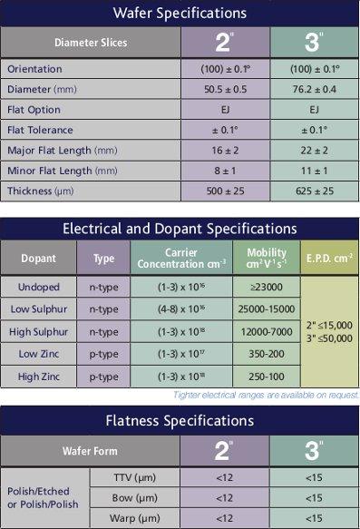
1 GaAs - Gallium Arsenide MECHANICAL SPECIFICATIONS Gallium Arsenide can be supplied in as-cut, etched or polished wafer forms. All slices are individually laser scribed with ingot and slice identity to ensure perfect traceability. ORIENTATION SPECIFICATIONS Surface orientations are offered to an accuracy of +/ degrees using a triple axis X-Ray diffractometer system. Substrates can also be supplied with very precise misorientations in any direction from the growth plane. Higher index substrates of the type (n,1,1) where n = 1,2,3,4,5,6 etc and orientations such as (110) are also available. We also offer wafers with cut and/or cleaved flats. SURFACE SPECIFICATIONS All wafers are offered with high quality epitaxy ready finishing. Surfaces are characterised by in-house, advanced optical metrology techniques which include Surfscan haze and particle monitoring, spectroscopic ellipsometry and grazing incidence interferometry. PACKAGING Polished Wafers coin-style tray, individually sealed in two outer bags in inert atmosphere. Cassette shipments are available on request). As-cut Wafers Cassette shipment. (Glassine bag available on request). 'Process Trial' wafers Packaged in coin-style wafer shipper, individually sealed in one outer bag.

2
3 GaSb - Gallium Antimonide MECHANICAL SPECIFICATIONS Gallium Antimonide is supplied in polished wafer form. All slices are individually laser scribed with ingot and slice identity to ensure perfect traceability. ORIENTATION SPECIFICATIONS Surface orientations are offered to an accuracy of +/ degrees using a triple axis X-Ray diffractometer system. Substrates can also be supplied with very precise misorientations in any direction from the growth plane. Higher index substrates of the type (n,1,1) where n = 1,2,3,4,5,6 etc and orientations such as (110) are also available. We also offer wafers with cut and/or cleaved flats. SURFACE SPECIFICATIONS All wafers are offered with high quality epitaxy ready finishing. Surfaces are characterised by in-house, advanced optical metrology techniques which include Surfscan haze and particle monitoring, spectroscopic ellipsometry and grazing incidence interferometry. PACKAGING Polished Wafers coin-style tray, individually sealed in two outer bags in inert atmosphere. Cassette shipments are available on request). As-cut Wafers

4 Cassette shipment. (Glassine bag available on request). 'Process Trial' wafers Packaged in coin-style wafer shipper, individually sealed in one outer bag.
5 InP - Indium Phosphide MECHANICAL SPECIFICATIONS Indium Phosphide can be supplied in as-cut, etched or polished wafer forms. All slices are individually laser scribed with ingot and slice identity to ensure perfect traceability. ORIENTATION SPECIFICATIONS Surface orientations are offered to an accuracy of +/ degrees using a triple axis X-Ray diffractometer system. Substrates can also be supplied with very precise misorientations in any direction from the growth plane. Higher index substrates of the type (n,1,1) where n = 1,2,3,4,5,6 etc and orientations such as (110) are also available. We also offer wafers with cut and/or cleaved flats. SURFACE SPECIFICATIONS All wafers are offered with high quality epitaxy ready finishing. Surfaces are characterised by in-house, advanced optical metrology techniques which include Surfscan haze and particle monitoring, spectroscopic ellipsometry and grazing incidence interferometry. PACKAGING Polished Wafers coin-style tray, individually sealed in two outer bags in inert atmosphere. Cassette shipments are available on request). As-cut Wafers

6 Cassette shipment. (Glassine bag available on request). 'Process Trial' wafers Packaged in coin-style wafer shipper, individually sealed in one outer bag.
7 InSb - Indium Antimonide MECHANICAL SPECIFICATIONS Indium Antimonide is supplied in polished wafer form. All slices are individually laser scribed with ingot and slice identity to ensure perfect traceability. ORIENTATION SPECIFICATIONS Surface orientations are offered to an accuracy of +/ degrees using a triple axis X-Ray diffractometer system. Substrates can also be supplied with very precise misorientations in any direction from the growth plane. Higher index substrates of the type (n,1,1) where n = 1,2,3,4,5,6 etc and orientations such as (110) are also available. We also offer wafers with cut and/or cleaved flats. SURFACE SPECIFICATIONS All wafers are offered with high quality epitaxy ready finishing. Surfaces are characterised by in-house, advanced optical metrology techniques which include Surfscan haze and particle monitoring, spectroscopic ellipsometry and grazing incidence interferometry. PACKAGING Polished Wafers coin-style tray, individually sealed in two outer bags in inert atmosphere. Cassette shipments are available on request). As-cut Wafers Cassette shipment. (Glassine bag available on request). 'Process Trial' wafers Packaged in coin-style wafer shipper, individually sealed in one outer bag.

8
9 InAs - Indium Arsenide MECHANICAL SPECIFICATIONS Indium Arsenide can be supplied as ingot sections or as-cut, etched or polished wafers. All slices are individually laser scribed with ingot and slice identity to ensure perfect traceability. ORIENTATION SPECIFICATIONS Surface orientations are offered to an accuracy of +/ degrees using a triple axis X-Ray diffractometer system. Substrates can also be supplied with very precise misorientations in any direction from the growth plane. Higher index substrates of the type (n,1,1) where n = 1,2,3,4,5,6 etc and orientations such as (110) are also available. We also offer wafers with cut and/or cleaved flats. SURFACE SPECIFICATIONS All wafers are offered with high quality epitaxy ready finishing. Surfaces are characterised by in-house, advanced optical metrology techniques which include Surfscan haze and particle monitoring, spectroscopic ellipsometry and grazing incidence interferometry. PACKAGING Polished Wafers coin-style tray, individually sealed in two outer bags in inert atmosphere. Cassette shipments are available on request). As-cut Wafers Cassette shipment. (Glassine bag available on request). 'Process Trial' wafers Packaged in coin-style wafer shipper, individually sealed in one outer bag.
10
Gallium Arsenide monocrystalline
 Gallium Arsenide CMK manufacture Semi-insulating and Semiconducting Gallium Arsenide wafers and ingots by LEC (Liquid Encapsulated Czochralsky) or VGF (Vertical Gradient Freeze) growth method. Required
id : class06 passwd: class06
 http://wwwee.stanford.edu/class_directory.php http://ocw.mit.edu/ocwweb/index.htm http://nanosioe.ee.ntu.edu.tw id : class06 passwd: class06 Display and OLED Market OLED on glass only ~US$ 0.5B in 04,
Certificate. Standard Reference Material Standard Sapphire Single Crystal Wafer for Crystalline Orientation
 National Institute of Standards & Technology Certificate Standard Reference Material 1995 Standard Sapphire Single Crystal Wafer for Crystalline Orientation This Standard Reference Material (SRM) is intended
Automating Hybrid Circuit Assembly
 Automating Hybrid Circuit Assembly Die Attach The demand for hybrid circuits has remained strong as emerging and existing applications continue to rely on this proven technology. Developers of applications
Bulk crystal growth. A reduction in Lg will increase g m and f oper but with some costs
 Bulk crystal growth The progress of solid state device technology has depended not only on the development of device concepts but also on the improvement of materials. A reduction in Lg will increase g
Data in Science and Technology. Editor in Chief: R. Poerschke. Editor: O. Madelung
 Data in Science and Technology Editor in Chief: R. Poerschke Semiconductors Group IV Elements and III -V Compounds Editor: O. Madelung Springer-Verlag Berlin Heidelberg New York London Paris Tokyo Hong
LANDOLT-BORNSTEIN. Zahlenwerte und Funktionen aus Naturwissenschaften und Technik. Neue Serie. Gesamtherausgabe: K.-H. Hellwege
 LANDOLT-BORNSTEIN Zahlenwerte und Funktionen aus Naturwissenschaften und Technik Neue Serie Gesamtherausgabe: K.-H. Hellwege Gruppe III: Kristall- und Festkörperphysik Band 17 Halbleiter Herausgeber: O.
Physics and Material Science of Semiconductor Nanostructures
 Physics and Material Science of Semiconductor Nanostructures PHYS 570P Prof. Oana Malis Email: omalis@purdue.edu Today Bulk semiconductor growth Single crystal techniques Nanostructure fabrication Epitaxial
Wolfspeed SiC and GaN Materials Catalog
 Wolfspeed SiC and GaN Materials Catalog Wolfspeed SiC and GaN Materials Industry-Leading Portfolio, Innovation and Scale Wolfspeed is a fully integrated materials supplier with the largest and most diverse
Fabrication Technology
 Fabrication Technology By B.G.Balagangadhar Department of Electronics and Communication Ghousia College of Engineering, Ramanagaram 1 OUTLINE Introduction Why Silicon The purity of Silicon Czochralski
Landolt-B örnstein Numerical Data and Functional Relationships in Science and Technology New Series I Editor in Chief: W.
 Landolt-B örnstein Numerical Data and Functional Relationships in Science and Technology New Series I Editor in Chief: W. Martienssen Group III: Condensed Matter Volume 41 Semiconductors Supplement to
TFS PRODUCTION SOLUTIONS. TFS Production Solutions. For thin-film solar modules
 TFS PRODUCTION SOLUTIONS TFS Production Solutions For thin-film solar modules 2 TFS PRODUCTION SOLUTIONS MANZ AG 3 TFS PRODUCTION SOLUTIONS MANZ AG GERMAN ENGINEERING INTERNATIONALLY STAGED GLOBAL REFERENCES
Optical Characterization of Epitaxial Semiconductor Layers
 Günther Bauer Wolfgang Richter (Eds.) Optical Characterization of Epitaxial Semiconductor Layers With 271 Figures Springer Contents Contributors XV 1 Introduction 1 Günther Bauer, Wolfgang Richter 2 Analysis
TFS PRODUCTION SOLUTIONS. TFS Production Solutions. For thin-film solar modules
 TFS PRODUCTION SOLUTIONS TFS Production Solutions For thin-film solar modules 2 TFS PRODUCTION SOLUTIONS MANZ AG 3 TFS PRODUCTION SOLUTIONS MANZ AG GERMAN ENGINEERING INTERNATIONALLY STAGED GLOBAL REFERENCES
Nanotechnology makes brighter LED s. Michael P.C. Watts
 Nanotechnology makes brighter LED s Michael P.C. Watts www.impattern.com Outline Why are LED s such a big deal? Brightness; lumens per watt & lumens per dollar Applications How does nanotechnology help?
1.3 Semiconducting materials
 8 Introduction Fig. 1.7 Periodic table of elements. Si and Ge in group IV, for example, are elementary semiconductors. Compound semiconductors contain, for example, elements from groups III and V, or II
TOWARD MEMS!Instructor: Riadh W. Y. Habash
 TOWARD MEMS!Instructor: Riadh W. Y. Habash Students are presented with aspects of general production and manufacturing of integrated circuit (IC) products to enable them to better liaise with and participate
Assignment Questions
 HIGH SPEED DEVICES AND CIRCUITS Assignment Questions 1) Why Silicon Semiconductors are widely used in the VLSI applications? Hint: Refer Video on Introduction to Basic Concepts 2) What are the parameters
Halbleiter Prof. Yong Lei Prof. Thomas Hannappel
 Halbleiter Prof. Yong Lei Prof. Thomas Hannappel yong.lei@tu-ilmenau.de thomas.hannappel@tu-ilmenau.de http://www.tu-ilmenau.de/nanostruk/ Solid State Structure of Semiconductor Semiconductor manufacturing
A discussion of crystal growth, lithography, etching, doping, and device structures is presented in
 Chapter 5 PROCESSING OF DEVICES A discussion of crystal growth, lithography, etching, doping, and device structures is presented in the following overview gures. SEMICONDUCTOR DEVICE PROCESSING: AN OVERVIEW
The components of. Technology focus: III-Vs on silicon. Fiber-optic gallium antimonide
 76 Direct growth of III-V laser structures on silicon substrates From infrared to ultraviolet wavelengths, researchers are enabling lower-cost production of silicon photonics. Mike Cooke reports. The components
THE NEXT GENERATION OF GERMANIUM SUBSTRATES: EXPOGER
 THE NEXT GENERATION OF GERMANIUM SUBSTRATES: EXPOGER Pieter Arickx (1), Rufi Kurstjens (1), Wim Geens (1), Kristof Dessein (1) (1) Umicore Electro-Optic Materials, Watertorenstraat 33 B2250 Olen (Belgium),
MOCVD Technology for LED
 MOCVD Technology for LED Prof. Dr.-Ing. Michael Heuken Vice President Corporate Research and Development AIXTRON AG, Fon: +49 (241) 8909-154, Fax: +49 (241) 8909-149, Email: M.Heuken@AIXTRON.com RWTH Aachen,
Semiconductor Optoelectronics Prof. M. R. Shenoy Department of Physics Indian Institute of Technology, Delhi. Lecture - 10 Semiconductor Materials
 Semiconductor Optoelectronics Prof. M. R. Shenoy Department of Physics Indian Institute of Technology, Delhi Lecture - 10 Semiconductor Materials Today we will discuss about semiconductor materials in
This lecture is part of the Basic XRD Course.
 This lecture is part of the Basic XRD Course. Basic XRD Course 1 A perfect polycrystalline sample should contain a large number of crystallites. Ideally, we should always be able to find a set of crystallites
Background Statement for SEMI Draft Document 4979 New Standard: SPECIFICATION FOR POLISHED MONOCRYSTALLINE GALLIUM NITRIDE WAFERS
 Background Statement for SEMI Draft Document 4979 New Standard: SPECIFICATION FOR POLISHED MONOCRYSTALLINE GALLIUM NITRIDE WAFERS NOTICE: This background statement is not part of the balloted item. It
Crystalline Silicon Solar Cells
 12 Crystalline Silicon Solar Cells As we already discussed in Chapter 6, most semiconductor materials have a crystalline lattice structure. As a starting point for our discussion on crystalline silicon
SOI: Challenges and Solutions to Increasing Yield in an Ultrathin Age
 New S U B S TIdeas R A T E Sfor New Materials SOI: Challenges and Solutions to Increasing Yield in an Ultrathin Age Christophe Maleville and George Celler, Soitec Silicon-on-insulator (SOI) wafers are
Making of a Chip Illustrations
 Making of a Chip Illustrations 22nm 3D/Trigate Transistors Version April 2015 1 The illustrations on the following foils are low resolution images that visually support the explanations of the individual
E. Buffagni, C. Ferrari, L. Zanotti, A. Zappettini
 E. Buffagni, C. Ferrari, L. Zanotti, A. Zappettini IMEM-CNR Institute, Parma (Italy) 1. Laue lenses for hard x-ray astronomy 2. Mosaic crystals 3. GaAs crystals 4. X-ray diffraction characterization 5.
GROWTH AND INVESTIGATION OF INDIUM ARSENIDE BASED DIODE HETEROSTRUCTURES FOR MID INFRARED APPLICATION
 GROWTH AND INVESTIGATION OF INDIUM ARSENIDE BASED DIODE HETEROSTRUCTURES FOR MID INFRARED APPLICATION V.A. Gevorkyan, K.M. Gambaryan, and M.S. Kazaryan Yerevan State University, E-mail: vgev@ysu.am 1.
Modification of Deposition Process Parameters for Uniform Indium Layer Deposition
 Old Dominion University ODU Digital Commons Electrical & Computer Engineering Theses & Disssertations Electrical & Computer Engineering Spring 2017 Modification of Deposition Process Parameters for Uniform
SINGLE CRYSTAL SAPPHIRE
 SINGLE CRYSTAL SAPPHIRE Single Crystal Sapphire plays an everincreasingly important role as a material for high reliability Opto-Electronics today due to excellent mechanical characteristics, chemical
Semiconductor Optical Communication Components and Devices Lecture 8: Epitaxial growth - I (Techniques)
") Semiconductor Optical Communication Components and Devices Lecture 8: Epitaxial growth - I (Techniques) Prof. Utpal Das Professor, Department of Electrical Engineering, Laser Technology Program, Indian
Semiconductor Optical Communication Components and Devices Lecture 8: Epitaxial growth - I (Techniques) Prof. Utpal Das Professor, Department of Electrical Engineering, Laser Technology Program, Indian
Thermal Oxidation and Growth of Insulators (Chapter 3 - Jaeger 3) Key advantage of Si: Oxidation of Si into SiO 2 (glass) Major factor in making
 Key advantage of Si: Oxidation of Si into SiO 2 (glass) Major factor in making") Thermal Oxidation and Growth of Insulators (Chapter 3 - Jaeger 3) Key advantage of Si: Oxidation of Si into SiO (glass) Major factor in making Silicon the main semiconductor Grown at high temperature in
Thermal Oxidation and Growth of Insulators (Chapter 3 - Jaeger 3) Key advantage of Si: Oxidation of Si into SiO (glass) Major factor in making Silicon the main semiconductor Grown at high temperature in
SPI Supplies Brand MgO Magnesium Oxide Single Crystal Substrates, Blocks, and Optical Components
 SPI Supplies Brand MgO Magnesium Oxide Single Crystal Substrates, Blocks, and Optical Components Used by high temperature thin film superconductor researchers worldwide! Purity better than 99.9%! Choose
ELEC 3908, Physical Electronics, Lecture 4. Basic Integrated Circuit Processing
 ELEC 3908, Physical Electronics, Lecture 4 Basic Integrated Circuit Processing Lecture Outline Details of the physical structure of devices will be very important in developing models for electrical behavior
High-Speed Infrared Imaging for Characterization of the Additive Manufacturing Process
 14 th Quantitative InfraRed Thermography Conference High-Speed Infrared Imaging for Characterization of the Additive Manufacturing Process by M.A. Langevin*, A. Huot*, S. Boubanga*, P. Lagueux*, E. Guyot*
MRSI-M1 1-Micron Die Bonder
 MRSI-M1 1-Micron Die Bonder Assembly Technologies: Eutectic Bonding Epoxy Component Attach In-situ UV Bonding Flip Chip Assembly Thermal Compression Bonding Overview The MRSI-M1 1-Micron Die Bonder builds
Hydrogen in Crystalline Semiconductors r
 S.J. Pearton J.W Corbett M. Stavola Hydrogen in Crystalline Semiconductors r ' With 250 Figures Springer-Verlag Berlin Heidelberg New York London Paris Tokyo Hong Kong Barcelona Budapest Contents 1. Introduction
Maintenance and Use of the MICROPOSITION PROBE
 Maintenance and Use of the MICROPOSITION PROBE Application Measurement of resistivity of samples by the four point technique using a Jandel four point probe head a) Where the probe needles need to be positioned
surface metrology. As the world s leader in precise, noncontact, 3-D surface metrology, Zygo has continually
 N E W V I E W 5 0 0 0 As the world s leader in precise, noncontact, 3-D surface metrology, Zygo has continually provided new advanced measurement capabilities to its existing line of powerful and reliable
Processing of Semiconducting Materials Prof. Pallab Benerji Department of Materials Science Center Indian Institute of Technology, Kharagpur
 Processing of Semiconducting Materials Prof. Pallab Benerji Department of Materials Science Center Indian Institute of Technology, Kharagpur Lecture - 11 Compound Semiconductors (Refer Slide Time: 00:20)
Alternate Channel Materials for High Mobility CMOS
 Alternate Channel Materials for High Mobility CMOS By Christopher Henderson This year s International Electron Device Meeting (IEDM) discussed a wide range of approaches for creating CMOS transistors with
Automated, reliable lapping and polishing systems make light work of hard silicon carbide and sapphire wafers
 Automated, reliable lapping and polishing systems make light work of hard silicon carbide and sapphire wafers Author: Mark Kennedy www.logitech.uk.com Overview The lapping and polishing of wafers made
Controlling Heat and Mass Transport during the Vertical Bridgman Growth of Homogeneous Ternary III-V Semiconductor Alloys
 Trans. Indian Inst. Met. Vol.60, Nos. 2-3, April-June 2007, pp. 155-160 TP 2117 Controlling Heat and Mass Transport during the Vertical Bridgman Growth of Homogeneous Ternary III-V Semiconductor Alloys
Silicon Carbide Substrates and Epitaxy
 MAT-CATALOG.00K Silicon Carbide Substrates and Epitaxy Product Specifications 4H Silicon Carbide Substrates N-type and Semi-Insulating 6H Silicon Carbide Substrates N-type N-type and P-type Epitaxy Subject
First Electrically Pumped Hybrid Silicon Laser
 First Electrically Pumped Hybrid Silicon Laser UCSB Engineering Insights Oct 18 th 2006 Mario Paniccia Intel Corporation 1 Sept 18 th 2006 What We are Announcing Research Breakthrough: 1st Electrically
Precision Optical Engineering
 Precision Optical Engineering Products: Prisms Windows Mirrors Flats and Master angles Sight Glasses Key Features: Prisms (Contacted, Cemented, AR coated, Mounted) Windows (Flat, wedged, curved, drilled,
CHAPTERS SUMMARY OF RESULTS
 CHAPTERS SUMMARY OF RESULTS Aluminium diffusion was investigated by NRA in five different semiconductors. Different experimental methods were employed. For in-diffusion investigation thin aluminium films
CHAPTER 4 LED LIGHT EMITTING DIODE
 CHAPTER 4 LED LIGHT EMITTING DIODE 1 PART II LIGHT EMITTING DIODE LED are semiconductor p-n junctions that under forward bias conditions can emit What is LED? radiation by electroluminescence in the UV,
Passivation of InAs and GaSb with novel high dielectrics
 Passivation of InAs and GaSb with novel high dielectrics Professor Minghwei HONG Department of Materials Science and Engineering, National Tsing Hua University 101, Section 2, Kuang-Fu Rd., Hsinchu, Taiwan,
Precision Without Compromise
 D1 EVOLUTION Precision Without Compromise Versatile and user-friendly high resolution and multipurpose X-ray diffractometer for the characterization of advanced materials www.jvsemi.com D1 Overview Introduction
Handbook of Optical Constants of Solids
 Handbook of Optical Constants of Solids Edited by EDWARD D. PALIK Naval Research Laboratory Washington, D.C. ACADEMIC PRESS, INC. Harcourt Brace Jovanovich, Publishers Boston San Diego New York London
Development Status of EUVL Blank and Substrate Asahi Glass Co. Ltd. Kazunobu Maeshige
 Development Status of EUVL Blank and Substrate Asahi Glass Co. Ltd. Kazunobu Maeshige 1 Contents 1. Introduction 2. Blank defect reduction 1. Inspection capability 2. Substrate 3. ML blank 4. Absorber
Safe Harbor Statement
 May June 2013 Safe Harbor Statement Certain statements in this presentation relate to future results that are forward-looking statements as defined in the Private Securities Litigation Reform Act of 1995.
Lecture 6. Monocrystalline Solar Cells
 Lecture 6 Monocrystalline Solar Cells References: 1. Physics of Solar Cells. Jenny Nelson. Imperial College Press, 2003. 2. Photovoltaic Materials, Series on Properties of Semiconductor Materials, Vol.1,
enabling tomorrow s technologies CVD Production Systems for Industrial Coatings powered by
 enabling tomorrow s technologies CVD Production Systems for Industrial Coatings powered by www.cvdequipment.com Equipment Design, Engineering, and Manufacturing Thin film deposition systems for industrial
Background Statement for SEMI Draft Document 4806 New Standard: GUIDE TO DEFECTS FOUND ON MONOCRYSTALLINE SILICON CARBIDE SUBSTRATES
 Background Statement for SEMI Draft Document 4806 New Standard: GUIDE TO DEFECTS FOUND ON MONOCRYSTALLINE SILICON CARBIDE SUBSTRATES NOTICE: This background statement is not part of the balloted item.
P.S. Dutta Introduction
 1 12 Crystal-Growth Technology for Ternary III-V Semiconductor Production by Vertical Bridgman and Vertical Gradient Freezing Methods with Accelerated Crucible Rotation Technique P.S. Dutta 12.1 Introduction
Spatially Resolved X-ray Diffraction Technique for Crystallographic Quality Inspection of Semiconductor Microstructures
 Vol. 114 (2008) ACTA PHYSICA POLONICA A No. 5 Proc. XXXVII International School of Semiconducting Compounds, Jaszowiec 2008 Spatially Resolved X-ray Diffraction Technique for Crystallographic Quality Inspection
PY2N20 Material Properties and Phase Diagrams
 PY2N20 Material Properties and Phase Diagrams Lecture 9 P. Stamenov, PhD School of Physics, TCD PY2N20-9 Semiconductor Wafer Production - Si Czochralski Growth Growth from melt Melt 99.999999% pure polycrystalline
Basics of Solar Photovoltaics. Photovoltaics (PV) Lecture-21
 Lecture-21") Lecture-21 Basics of Solar Photovoltaics Photovoltaics (PV) Photovoltaics (PV) comprise the technology to convert sunlight directly into electricity. The term photo means light and voltaic, electricity.
Lecture-21 Basics of Solar Photovoltaics Photovoltaics (PV) Photovoltaics (PV) comprise the technology to convert sunlight directly into electricity. The term photo means light and voltaic, electricity.
Figure 6. Rare-gas atom-beam diffraction patterns. These results were obtained by Wieland Schöllkopf and Peter Toennies at the Max-Planck Institute
 Figure 6. Rare-gas atom-beam diffraction patterns. These results were obtained by Wieland Schöllkopf and Peter Toennies at the Max-Planck Institute in Göttingen, Germany, using a freestanding, 100nm-period
Applications Et Realisations De La Technologie Plasma Reactive Atom Plasma (RAP) Pour La Fabrication De Grands Optiques R. Jourdain, M. Castelli, P.
 Pour La Fabrication De Grands Optiques R. Jourdain, M. Castelli, P.") Applications Et Realisations De La Technologie Plasma Reactive Atom Plasma (RAP) Pour La Fabrication De Grands Optiques R. Jourdain, M. Castelli, P. Morantz, P. Shore Cranfield University, Precision Engineering
Applications Et Realisations De La Technologie Plasma Reactive Atom Plasma (RAP) Pour La Fabrication De Grands Optiques R. Jourdain, M. Castelli, P. Morantz, P. Shore Cranfield University, Precision Engineering
Preparation of Gallium Antimonide and its Characterization
 Material Science Research India Vol. 12(1), 31-35 (2015) Preparation of Gallium Antimonide and its Characterization J.Chidanandappa 1, K. Eswara Prasad 2, K. Balaraju 3 and V. N. MANI 3 1 National Remote
LANDOLT-BÖRNSTEIN. Zahlenwerte und Funktionen aus Naturwissenschaften und Technik. Neue Serie. Gesamtherausgabe: O. Madelung
 LANDOLT-BÖRNSTEIN Zahlenwerte und Funktionen aus Naturwissenschaften und Technik Neue Serie Gesamtherausgabe: O. Madelung Gruppe III: Kristall- und Festkörperphysik Band 22 Halbleiter Ergänzungen und Erweiterungen
HIGH-RESOLUTION X-RAY DIFFRACTION OF EPITAXIAL LAYERS ON VICINAL SEMICONDUCTOR SUBSTRATES
 Philips J. Res. 47 (1993) 203-215 HIGH-RESOLUTION X-RAY DIFFRACTION OF EPITAXIAL LAYERS ON VICINAL SEMICONDUCTOR SUBSTRATES by P. VAN DER SLUIS Philips Research Laboratories, P'I), Box 80000.5600 JA Eindhoven.
Development of High-concentration Photovoltaics at Fraunhofer ISE: Cells and Systems
 Development of High-concentration Photovoltaics at Fraunhofer ISE: Cells and Systems Gerhard Peharz Fraunhofer-Institut für Solare Energiesysteme ISE 23 rd October 2008 Outline The Fraunhofer ISE III-V
PHYSICAL PROPERTIES OF AlGaAs EPILAYERS SUBJECTED TO HIGH PRESSURE HIGH TEMPERATURE TREATMENT
 Vol. 91 (1997) ACTA PHYSICA POLONICA A No. 5 Proceedings of the 3rd ISSSRNS Jaszowiec'96 PHYSICAL PROPERTIES OF AlGaAs EPILAYERS SUBJECTED TO HIGH PRESSURE HIGH TEMPERATURE TREATMENT W. SZUSZKIEWICZa,
REPORT DOCUMENTATION PAGE. 4.IUUIU111 lu S. MONITORING ORGANIZATION REPORT NUMIEWC
 REPORT DOCUMENTATION PAGE In. REPORT SECURITY CLASSIFICATION 1b. RIESTRICTIVE PKW Unclassified Nonrb 2&. SECURITY CLASSIFICATION AITI^0"1 3. DISTRITINAVAJAIjrV OF REPORT Approved for public release 2 A
X-RAY DIFFRACTION IN SEMICONDUCTOR INDUSTRY AND RESEARCH
 X-RAY DIFFRACTION IN SEMICONDUCTOR INDUSTRY AND RESEARCH M. Leszczyński High Pressure Research Center UNIPRESS, Sokolowska 29/37, 01 142 Warsaw, Poland, e-mail: mike@unipress.waw.pl ABSTRACT The paper
Table of Contents by Topic
 Table of Contents by Topic 0114 NOTICE: Starting with the November 2001 (1101) publishing cycle, a distinction is being made between Standards that have subordinate document designation numbers and require
Manufacturing Technologies for MEMS and SMART SENSORS
 4 Manufacturing Technologies for MEMS and SMART SENSORS Dr. H. K. Verma Distinguished Professor (EEE) Sharda University, Greater Noida (Formerly: Deputy Director and Professor of Instrumentation Indian
Table of Contents by Topic
 Table of Contents by Topic 0614 NOTICE: Starting with the November 2001 (1101) publishing cycle, a distinction is being made between Standards that have subordinate document designation numbers and require
United States Patent (19)
") United States Patent (19) Jiang et al. 54) VERTICAL CAVITY SURFACE EMITTING LASER FOR HIGH POWER SINGLE MODE OPERATION AND METHOD OF FABRICATION 75 Inventors: Wenbin Jiang, Phoenix; Rong-Ting Huang, Gilbert;
United States Patent (19) Jiang et al. 54) VERTICAL CAVITY SURFACE EMITTING LASER FOR HIGH POWER SINGLE MODE OPERATION AND METHOD OF FABRICATION 75 Inventors: Wenbin Jiang, Phoenix; Rong-Ting Huang, Gilbert;
Factory of the Future; Additive Manufacturing. Jon Porter Business Development AMSC
 Factory of the Future; Additive Manufacturing Jon Porter Business Development AMSC About Renishaw World leading metrology & engineering company A FTSE 250 company with headquarters in United Kingdom Advancing
C a r d if f UNIVERSITY
 C a r d if f UNIVERSITY PR I FYSCOL C a 'R D v^ BINDING SERVICES Tel +44 (0)29 2087 4949 Fax+44 (0)29 20371921 e-mail bindery@cardiff.ac.uk Cross-Sectional Atomic Force Microscopy of lll-v Semiconductor
Sample Preparation Procedure for TEM Imaging of Semiconductor Materials
 Sample Preparation Procedure for TEM Imaging of Semiconductor Materials by Wendy L. Sarney ARL-TR-3223 June 2004 Approved for public release; distribution unlimited. NOTICES Disclaimers The findings in
MRSI-M3 3-Micron Die Bonder
 MRSI-M3 3-Micron Die Bonder Assembly Technologies: Eutectic Bonding Epoxy Component Attach In-situ UV Bonding Flip Chip Assembly Thermal Compression Bonding Applications: MEMS Multi-Chip Modules Semiconductor
Course Outline ENSC495/851: Introduction to Microelectronic Fabrication (ENSC 495, 4 credits, 2-0-4: ENSC 851, 3 credits, 2-0-1)
") Course Outline 2014-1 ENSC495/851: Introduction to Microelectronic Fabrication (ENSC 495, 4 credits, 2-0-4: ENSC 851, 3 credits, 2-0-1) Professor: Glenn Chapman, Rm ASB 8831, Phone: 778-782-3814, email:
Course Outline 2014-1 ENSC495/851: Introduction to Microelectronic Fabrication (ENSC 495, 4 credits, 2-0-4: ENSC 851, 3 credits, 2-0-1) Professor: Glenn Chapman, Rm ASB 8831, Phone: 778-782-3814, email:
This document should be superseded by dimensional specification and technology-specific guidelines for circuit-quality wafers.
 Background Statement for SEMI Document 4624B (rev. 16) NEW STANDARD: SPECIFICATION FOR DEVELOPMENTAL 450 mm DIAMETER POLISHED SINGLE CRYSTAL SILICON WAFERS Note: This background statement is not part of
In Vivo Applications of Near-Infrared Quantum Dots
 In Vivo Applications of Near-Infrared Quantum Dots John V. Frangioni, M.D., Ph.D. Assistant Professor of Medicine Assistant Professor of Radiology Harvard Medical School Moungi G. Bawendi, Ph.D. Professor
Scribing-Cleaving-Passivation for High Energy Physics Silicon Sensors
 Scribing-Cleaving-Passivation for High Energy Physics Silicon Sensors Marc Christophersen 1, Bernard F. Phlips 1, Vitaliy Fadeyev 2, Scott Ely 2, Hartmut F.-W. Sadrozinski 2 (1) Code 7654, U.S. Naval Research
Study on the impurities segregation behaviour during zone refining of indium
 Study on the impurities segregation behaviour during zone refining of indium V. N. Mani* and K. Balaraju Centre for Materials for Electronics Technology (C-MET), Cherlapally, Hyderabad 500 051, India ABSTRACT
Germanium and silicon photonics
 76 Technical focus: III-Vs on silicon optoelectronics Germanium and silicon photonics Mike Cooke reports on recent research using germanium to enable infrared light-emitting devices to be created on silicon
Monitoring epiready semiconductor wafers
 Thin Solid Films 412 (2002) 76 83 Monitoring epiready semiconductor wafers D.A. Allwood, S. Cox, N.J. Mason*, R. Palmer, R. Young, P.J. Walker Physics Department, Clarendon Laboratory, University of Oxford,
Glass Wafer. Specification
 Glass Wafer Specification Glass Wafer Specification SCHOTT Thin Glass and Wafer products are the result of deep technological expertise. With a product portfolio of more than 100 optical glasses, special
Specimen Preparation Technique for a Microstructure Analysis Using the Focused Ion Beam Process
 Specimen Preparation Technique for a Microstructure Analysis Using the Focused Ion Beam Process by Kozue Yabusaki * and Hirokazu Sasaki * In recent years the FIB technique has been widely used for specimen
Synchrotron x-ray topographic and high-resolution diffraction analysis of mask-induced strain in epitaxial laterally overgrown GaAs layers
 JOURNAL OF APPLIED PHYSICS VOLUME 86, NUMBER 8 15 OCTOBER 1999 Synchrotron x-ray topographic and high-resolution diffraction analysis of mask-induced strain in epitaxial laterally overgrown GaAs layers
Thin Film Scattering: Epitaxial Layers
 Thin Film Scattering: Epitaxial Layers 6th Annual SSRL Workshop on Synchrotron X-ray Scattering Techniques in Materials and Environmental Sciences: Theory and Application May 29-31, 2012 Thin films. Epitaxial
LED Production Yield Improvement Through Advanced In-Situ Metrology. Tom Thieme director marketing & sales
 LED Production Yield Improvement Through Advanced In-Situ Metrology Tom Thieme director marketing & sales 2 Outline - Introduction - In-situ metrology the concept - Up-time: fault detection and rapid root
At wavelength characterization of EUV and soft X-ray gratings
 At wavelength characterization of EUV and soft X-ray gratings F. Scholze, A, Haase, C. Laubis, V. Soltwisch, J. Wernecke, M. Krumrey Physikalisch-Technische Bundesanstalt, Abbestraße 2-12, 10587 Berlin,
MATERIALS J 01. MATERIALS / Inorganics & thin films guide
 J MATERIALS SUBSTRATES Silicon Wafers... J 04 Single Crystal Substrates... J 07 Glass & Fused Quartz Substrates... J 44 Ceramic Substrates... J 48 Glassy Carbon Substrates... J 49 HOPG & Mica Substrates...
MRSI Micron Die Bonder
 MRSI-705 5-Micron Die Bonder Assembly Technologies: Eutectic Bonding Epoxy Component Attach In-situ UV Bonding Flip Chip Assembly Thermal Compression Bonding Applications: 3D Packaging Wafer Scale Packaging
warwick.ac.uk/lib-publications
 A Thesis Submitted for the Degree of PhD at the University of Warwick Permanent WRAP URL: http://wrap.warwick.ac.uk/107946/ Copyright and reuse: This thesis is made available online and is protected by
High Resolution X-ray Diffraction Analysis of Gallium Nitride/Silicon Carbide Heterostructures H.M. Volz 1, R.J. Matyi 2, and J.M.
 Copyright ISSN (C) 197-2, JCPDS-International Advances in X-ray Centre Analysis, for Volume Diffraction 41 Data 1999 139 High Resolution X-ray Diffraction Analysis of Gallium Nitride/Silicon Carbide Heterostructures
MRSI Micron Die Bonder
 MRSI-705 5-Micron Die Bonder Assembly Technologies: Eutectic Bonding Epoxy Component Attach In-situ UV Bonding Flip Chip Assembly Thermal Compression Bonding Applications: 3D Packaging Wafer Scale Packaging
Enhanced Material Removal Rate For III/V Semiconductors
 Enhanced Material Removal Rate For III/V Semiconductors G. Bahar Basim, Sebnem Ozbek, Wazir Akbar Ozyegin University Department of Mechanical Engineering, Nisantepe Mevki, No 34-36, Cekmekoy, Istanbul,
MATERIALS. Silicon Wafers... J 04 J 01. MATERIALS / Inorganics & thin films guide
 J MATERIALS SUBSTRATES Silicon Wafers... J 04 J J 01 MATERIALS SUBSTRATES NEYCO has a complete range of crystal substrates for a wide variety of applications, including Semiconductor, Biotechnology, Nanotechnology,