Monte Carlo approach to island formation during thermal treatment of thin films*
|
|
|
- Dennis Strickland
- 6 years ago
- Views:
Transcription
1 Monte Carlo approach to island formation during thermal treatment of thin films* Ann Marie Hardin December 6, 2006 *F. Lallet, R. Bachelet, A. Dauger, and N. Olivi-Tran, (2006) Physical Review B, 74
2 Outline Background Monte Carlo Simulation of Thin Films Simulation Results Extended Investigations Conclusions
3 Thin Film Applications Electronic semiconductor Optical coatings Corrosion, oxidation and wear resistance Computer memory Photovoltaic cells
4 Challenges Physics of thin films are not completely understood Dewetting Island formation Effect of substrate inpurities Film thickness control
5 Methods of manufacture Dip coating Spin coating Sputtering Chemical Vapor Deposition Sol-gel
6 Methods of Manufacture All methods require coating of substrate surface with polymer film and then curing to form stable film
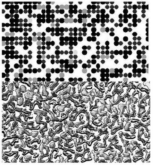
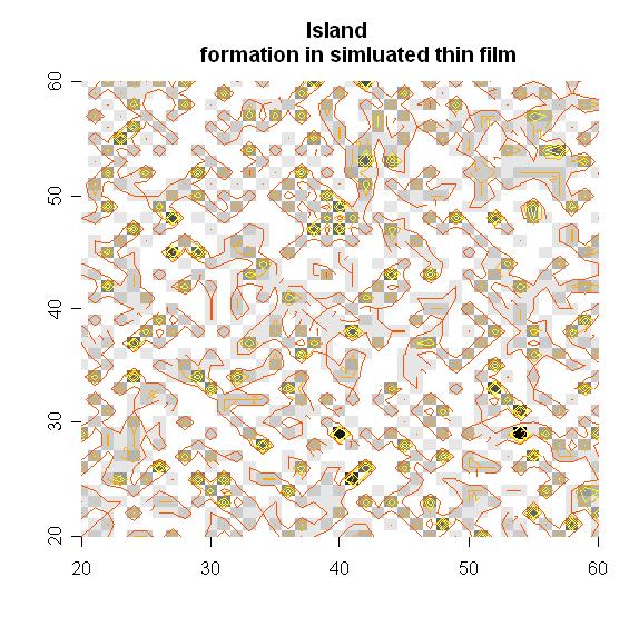
7 Island Formation Accompanied by dewetting During thermal treatment, areas of increased height form spontaneously in film Initial flat surface is a strained fromation Film stabilizes to lowest-energy configuration

8 Island Formation Zhang, Y. W., Self-organization, shape transition, and stability of epitaxially strained islands., Physical Review B. 61(15):
9 Simulation of Island Formation: a Monte Carlo Approach Surface modeled as array of square domains atoms per domain Initial film thickness is 1 nm Crystallographic orientation randomly assigned
10 Model Parameters Film thickness Crystallographic orientation related to inter-plane spacing Film energy Surface strain due to neighboring domains with different crystallographic orientation Interfacial energy between one domain and substrate Surface strain due to neighboring domains with different heights
11 Model Implentation Each domain owns three states Vertical interplane spacing ( ) Horizontal interplane spacing ( ) Domain height (0 4) Film energy given as sum of all domain state energies
12 Monte Carlo Algorithm Choose domain Propose new horizontal spacing Accept or reject proposed change Propose new vertical spacing Accept or reject proposed change
13 Monte Carlo Algorithm Choose neighbor of chosen domain Propose height exchange between two domains
14 Proposal Vertical and horizontal spacing Increase or decrease by 0.5 Bounded at 0.2 and 2.5 Reflect back to interior if at boundary. Domain height Target domain increased or decreased by 1 Neighbor changed by same amount but opposing direction
15 Acceptance criteria Calculate energy change associated with proposed configurational change E E E 2 1 Accept proposed change with probability P P 1, E 0 E kbt e, E 0
16 Calculation of Surface Energy E l B l c c l C l d d Dl h h 2 NN 2 NN NN i i i i j i i j i i j hi j 1 hi j 1 j 1 i 2 B scales interfacial energy between two domains C scales interfacial energy between a domain and the substrate D scales the surface strain between two neighboring domains of differing heights
17 Efficiency Chain requires 1 million steps 3 evaluations per step Effeciency is important Calculate energy only at affected domains, not entire film
18 Results
19 Island Formation z y x
20 Evolution of Film Thickness
21 Published evolution of domain height
22 Evolution of Interplane Spacing
23 Effect of various components Parameter B and C are symmetrical B scales horizontal effects C scales vertical effects Affect inter-plane spacing or crystallographic orientation D scales surface strain due to height differences Affects island height and formation
24 Effect of inter-plane surface strain
25 Effect of inter-plane surface strain
26 Effect of Surface Strain due to Height differences
27 Effect of Surface Strain due to Height differences B=C=10 5, D = 10-5 B=C= D=1
28 Effect of Curing Temperature on Film Thickness Domains h=0 h=1 h=2 h=3 h=
29 Effect of Curing Temperature on Crystallographic Orientation c=0.5 c=1.0 c=1.5 c=2.0 c=2.5 Temperature d=0.5 d=1.0 d=1.5 d=2.0 d=2.5 Temperature
30 Effect of Initial Film Thickness Evolution of domain height Number of domains h=0 nm h=1 nm h=2 nm h=3 nm h=4 nm 0 e+00 2 e+05 4 e+05 6 e+05 8 e+05 1 e+06 Monte Carlo Steps
31 Conclusions Islands will form spontaneously during thermal annealing of thin films Monte Carlo simulations can be used to study island formation I was able to approximate but not replicated published results
Verwey transition in Fe 3 O 4 thin films: Influence of oxygen stoichiometry and substrate-induced microstructure
 Verwey transition in Fe 3 O 4 thin films: Influence of oxygen stoichiometry and substrate-induced microstructure Physical Review B 90, 125142 (2014) Xiaozhe Zhang 20150403 Verwey transition Charge ordering
MATERIALS. Silicon Wafers... J 04 J 01. MATERIALS / Inorganics & thin films guide
 J MATERIALS SUBSTRATES Silicon Wafers... J 04 J J 01 MATERIALS SUBSTRATES NEYCO has a complete range of crystal substrates for a wide variety of applications, including Semiconductor, Biotechnology, Nanotechnology,
Micromachining AMT 2505
 Micromachining AMT 2505 Shanmuga Raja.B (BVB0912004) Module leader : Mr. Raja Hussain Introduction Micromachining are inherently connected to the evolution of Micro Electro Mechanical Systems (MEMS). Decades
Nucleation and growth of nanostructures and films. Seongshik (Sean) Oh
 Oh") Nucleation and growth of nanostructures and films Seongshik (Sean) Oh Outline Introduction and Overview 1. Thermodynamics and Kinetics of thin film growth 2. Defects in films 3. Amorphous, Polycrystalline
Nucleation and growth of nanostructures and films Seongshik (Sean) Oh Outline Introduction and Overview 1. Thermodynamics and Kinetics of thin film growth 2. Defects in films 3. Amorphous, Polycrystalline
Technology Drivers for Plasma Prior to Wire Bonding
 Technology Drivers for Plasma Prior to Wire Bonding James D. Getty Nordson MARCH Concord, CA, USA info@nordsonmarch.com Technology Drivers for Plasma Prior to Wire Bonding Page 1 ABSTRACT Advanced packaging
Morphology of Thin Aluminum Film Grown by DC Magnetron Sputtering onto SiO 2 on Si(100) Substrate
 Substrate") Morphology of Thin Aluminum Film Grown by DC Magnetron Sputtering onto SiO 2 on Si(1) Substrate Fan Wu Microelectronics Center, Medtronic Inc., Tempe, AZ 85261 James E. Morris Department of Electrical
Morphology of Thin Aluminum Film Grown by DC Magnetron Sputtering onto SiO 2 on Si(1) Substrate Fan Wu Microelectronics Center, Medtronic Inc., Tempe, AZ 85261 James E. Morris Department of Electrical
Ceramic Processing Research
 Journal of Ceramic Processing Research. Vol. 10, No. 4, pp. 536~540 (009) J O U R N A L O F Ceramic Processing Research Electrical and optical properties of MgO films deposited on soda lime glass by a
Preface Preface to First Edition
 Contents Foreword Preface Preface to First Edition xiii xv xix CHAPTER 1 MEMS: A Technology from Lilliput 1 The Promise of Technology 1 What Are MEMS or MST? 2 What Is Micromachining? 3 Applications and
much research (in physics, chemistry, material science, etc.) have been done to understand the difference in materials properties.
 have been done to understand the difference in materials properties.") 1.1: Introduction Material science and engineering Classify common features of structure and properties of different materials in a well-known manner (chemical or biological): * bonding in solids are classified
1.1: Introduction Material science and engineering Classify common features of structure and properties of different materials in a well-known manner (chemical or biological): * bonding in solids are classified
Macroscopic Arrays of Block Copolymers with Areal Densities of 10 Terbit/inch 2 and Beyond
 Macroscopic Arrays of Block Copolymers with Areal Densities of 10 Terbit/inch 2 and Beyond Soojin Park*, Dong Hyun Lee, Bokyung Kim, Sung Woo Hong Department of Polymer Science and Engineering, University
Tribological Characterization of Ti-WS2 Coating
 Tribological Characterization of Ti-WS2 Coating Prepared by Johans Restrepo 6 Morgan, Ste156, Irvine CA 92618 P: 949.461.9292 F: 949.461.9232 nanovea.com Today's standard for tomorrow's materials. 2010
Handbook Of Thin Film Deposition Processes And Techniques (materials And Processing Technology)
") Handbook Of Thin Film Deposition Processes And Techniques (materials And Processing Technology) R. Glang, in: Handbook of Thin Film Technology (L. I. Maissel and R. Glang, eds.) T. A. Delchar, Vacuum Physics
Handbook Of Thin Film Deposition Processes And Techniques (materials And Processing Technology) R. Glang, in: Handbook of Thin Film Technology (L. I. Maissel and R. Glang, eds.) T. A. Delchar, Vacuum Physics
Lattice Kinetic Monte Carlo: Building a bridge between ab-initio calculations and process simulation
 Lattice Kinetic Monte Carlo: Building a bridge between ab-initio calculations and process simulation Polycrystalline Materials E. Rubio, M. Jaraiz, L.A. Bailon, J. Barbolla, M.J. Lopez University of Valladolid,
Imperfections in the Atomic and Ionic Arrangements
 Objectives Introduce the three basic types of imperfections: point defects, line defects (or dislocations), and surface defects. Explore the nature and effects of different types of defects. Outline Point
Supporting Information. The alignment of thermally conducting nanotubes making. high-performance light-driving motors
 Supporting Information The alignment of thermally conducting nanotubes making high-performance light-driving motors Meng Liao, Hao Sun, Xin Tao, Xiaojie Xu, Zhi Li, Xuemei Fu, Songlin Xie, Lei Ye, Ye Zhang,
Influence of Underlayer on Crystallography and Roughness of Aluminum Nitride Thin Film Reactively Sputtered by Ion-Beam Kaufman Source
 Influence of Underlayer on Crystallography and Roughness of Aluminum Nitride Thin Film Reactively Sputtered by Ion-Beam Kaufman Source GABLECH Imrich 1,*, SVATOŠ Vojtěch 1,, PRÁŠEK Jan 1,, HUBÁLEK Jaromír
Inline Sputtering System for Heterojunction Cells
 GENERIS PVD Inline Sputtering System for Heterojunction Cells GENERIS PVD Inline Sputter System for ITO and Ag Deposition on Heterojunction Solar Cells Sputtering Technology at a Glance has delivered far
Effect of nanoimprinted surface relief on Si and Ge nucleation and ordering
 Microelectronics Journal 37 (2006) 1481 1485 www.elsevier.com/locate/mejo Effect of nanoimprinted surface relief on Si and Ge nucleation and ordering T.I. Kamins a,, A.A. Yasseri a,1, S. Sharma a,2, R.F.W.
Fabrication of Ru/Bi 4-x La x Ti 3 O 12 /Ru Ferroelectric Capacitor Structure Using a Ru Film Deposited by Metalorganic Chemical Vapor Deposition
 Mat. Res. Soc. Symp. Proc. Vol. 784 2004 Materials Research Society C7.7.1 Fabrication of Ru/Bi 4-x La x Ti 3 O 12 /Ru Ferroelectric Capacitor Structure Using a Ru Film Deposited by Metalorganic Chemical
FePd (216 Å) grown on (001) MgO. 2θ(deg)
 grown on (001) MgO. 2θ(deg)") Major Findings 1. FePd thin films The structural characterization of the films grown at various substrate temperatures (RT- 700 o C) was performed ex-situ using X-Ray Diffraction (XRD). The optimum substrate
Major Findings 1. FePd thin films The structural characterization of the films grown at various substrate temperatures (RT- 700 o C) was performed ex-situ using X-Ray Diffraction (XRD). The optimum substrate
Control of Grain Growth Process by a Local Heating Method
 Trans. JWRI, Vol.34 (2005), No.1 Control of Grain Growth Process by a Local Heating Method SHIBAYANAGI Toshiya *, TSUKAMOTO Masahiro** and ABE Nobuyuki * Abstract The present work deals with a preferential
"Thin Film Technology" "Physics of Thin Films"
 D r d "Thin Film Technology" "Physics of Thin Films" Contents: Preface 1. Introduction 1.1. General 1.2. History 1.3. Definition of Terms 1.4. Applications of Thin Film Technology 1.5. Deposition Methods
Epitaxial growth of (001) and (111) Ni films on MgO substrates
 and (111) Ni films on MgO substrates") Epitaxial growth of (001) and (111) Ni films on MgO substrates Rosa Alejandra Lukaszew 1, Vladimir Stoica, Ctirad Uher and Roy Clarke Physics Department, University of Michigan, Ann Arbor 1 Presently at
Epitaxial growth of (001) and (111) Ni films on MgO substrates Rosa Alejandra Lukaszew 1, Vladimir Stoica, Ctirad Uher and Roy Clarke Physics Department, University of Michigan, Ann Arbor 1 Presently at
Colossal Electroresistance in. (La 1-y Pr y ) 0.67 Ca 0.33 MnO 3. Rafiya Javed. July 29, Abstract
 0.67 Ca 0.33 MnO 3. Rafiya Javed. July 29, Abstract") Colossal Electroresistance in (La 1-y Pr y ) 0.67 Ca 0.33 MnO 3 Rafiya Javed July 29, 2010 Abstract At low temperatures, LaPrCaMnO3(LPCMO), a perovskite manganite, exhibits a coexistence of ferromagnetic
Colossal Electroresistance in (La 1-y Pr y ) 0.67 Ca 0.33 MnO 3 Rafiya Javed July 29, 2010 Abstract At low temperatures, LaPrCaMnO3(LPCMO), a perovskite manganite, exhibits a coexistence of ferromagnetic
Thin Film Gas Sensor. Nanoelectronics and MEMS Laboratory National Electronics and Computer Technology
 Ion-assisted E-beam E Evaporated Thin Film Gas Sensor A. Wisitsoraat,, A. A Tuantranont,, V. V Patthanasettakul, T. Lomas,, and P. Chindaudom Nanoelectronics and MEMS Laboratory National Electronics and
Fully-integrated, Bezel-less Transistor Arrays Using Reversibly Foldable Interconnects and Stretchable Origami Substrates
 Electronic Supplementary Material (ESI) for Nanoscale. This journal is The Royal Society of Chemistry 2016 Fully-integrated, Bezel-less Transistor Arrays Using Reversibly Foldable Interconnects and Stretchable
More on VLSI Fabrication Technologies. Emanuele Baravelli
 More on VLSI Fabrication Technologies Emanuele Baravelli Some more details on: 1. VLSI meaning 2. p-si epitaxial layer 3. Lithography 4. Metallization 5. Process timings What does VLSI mean, by the way?
ATOMIC LAYER DEPOSITION OF 2D TRANSITION METAL DICHALOGENIDES
 ATOMIC LAYER DEPOSITION OF 2D TRANSITION METAL DICHALOGENIDES Annelies Delabie, M. Caymax, B. Groven, M. Heyne, K. Haesevoets, J. Meersschaut, T. Nuytten, H. Bender, T. Conard, P. Verdonck, S. Van Elshocht,
Journal of Asian Scientific Research. SIGNIFICANCE OF SUBSTRATES AND BUFFER LAYERS IN CdTe THIN FILM SOLAR CELL FABRICATION N.
 Journal of Asian Scientific Research journal homepage: http://aessweb.com/journal-detail.php?id=5003 SIGNIFICANCE OF SUBSTRATES AND BUFFER LAYERS IN CdTe THIN FILM SOLAR CELL FABRICATION N. Dhar 1 ABSTRACT
Grazing Incidence X-Ray Diffraction of Longitudinal and Perpendicular Magnetic Recording Media for HDD
 Grazing Incidence X-Ray Diffraction of Longitudinal and Perpendicular Magnetic Recording Media for HDD Michio OHSAWA, Fuji Electric Corporate Research and Development, Ltd. ohsawa-michio@fujielectric.co.jp
and cost implications of corrosion, casting a spot light on the need for innovation in pipe coating materials and processes.
 A ccording to the Energy Information Administration s International Energy Outlook for 2006, world oil demand is expected to grow from 80 million barrels per day in 2003 to 98 million barrels per day in
Lecture 1A: Manufacturing& Layout
 Introduction to CMOS VLSI Design Lecture 1A: Manufacturing& Layout David Harris Harvey Mudd College Spring 2004 Steven Levitan Fall 2008 1 The Manufacturing Process For a great tour through the IC manufacturing
Latching Shape Memory Alloy Microactuator
 Latching Shape Memory Alloy Microactuator ENMA490, Fall 00 S. Cabrera, N. Harrison, D. Lunking, R. Tang, C. Ziegler, T. Valentine Outline Background Problem Project Development Design Evaluation Applications
X-RAY DIFFRACTION IN SEMICONDUCTOR INDUSTRY AND RESEARCH
 X-RAY DIFFRACTION IN SEMICONDUCTOR INDUSTRY AND RESEARCH M. Leszczyński High Pressure Research Center UNIPRESS, Sokolowska 29/37, 01 142 Warsaw, Poland, e-mail: mike@unipress.waw.pl ABSTRACT The paper
ZnO-based Transparent Conductive Oxide Thin Films
 IEEE EDS Mini-colloquium WIMNACT 32 ZnO-based Transparent Conductive Oxide Thin Films Weijie SONG Ningbo Institute of Material Technology and Engineering, Chinese Academy of Sciences, Ningbo, P. R. China
and Technology of Thin Films
 An Introduction to Physics and Technology of Thin Films This page is intentionally left blank An Introduction to Physics and Technology of Thin Films Alfred Wagendriste1 Institute of Applied and Technical
Grain Growth Modeling for Additive Manufacturing of Nickel Based Superalloys
 Grain Growth Modeling for Additive Manufacturing of Nickel Based Superalloys H. L. Wei 1, T. Mukherjee 1 and T. DebRoy 1 1 The Pennsylvania State University, University Park, PA, 16801, USA Why grain growth
Pulsed Laser Deposition of Epitaxial Titanium Nitride on Magnesium Oxide substrate
 Pulsed Laser Deposition of Epitaxial Titanium Nitride on Magnesium Oxide substrate By, Preetam ANBUKARASU UTRIP 2012 (1 st Crew) Under the Guidance of, Prof. Tetsuya HASEGAWA, Solid State Chemistry Lab,
EFFECT OF CRYSTALORIENTATIONIN OXIDATION PROCESS OF VLSI FABRICATION
 International Journal of Research in Engineering, Technology and Science, Volume VII, Special Issue, Feb 2017 www.ijrets.com, editor@ijrets.com, ISSN 2454-1915 EFFECT OF CRYSTALORIENTATIONIN OXIDATION
EE 330 Lecture 8. IC Fabrication Technology Part II. - Oxidation - Epitaxy - Polysilicon - Interconnects
 EE 330 Lecture 8 IC Fabrication Technology Part II - Oxidation - Epitaxy - Polysilicon - Interconnects Review from Last Time MOS Transistor Bulk Source Gate Drain p-channel MOSFET Lightly-doped n-type
Amorphous Silicon Solar Cells
 The Birnie Group solar class and website were created with much-appreciated support from the NSF CRCD Program under grants 0203504 and 0509886. Continuing Support from the McLaren Endowment is also greatly
Pre-treatment of low temperature GaN buffer layer deposited on AlN Si substrate by hydride vapor phase epitaxy
 Ž. Surface and Coatings Technology 131 000 465 469 Pre-treatment of low temperature GaN buffer layer deposited on AlN Si substrate by hydride vapor phase epitaxy Ha Jin Kim, Ho-Sun Paek, Ji-Beom Yoo Department
Metallization deposition and etching. Material mainly taken from Campbell, UCCS
 Metallization deposition and etching Material mainly taken from Campbell, UCCS Application Metallization is back-end processing Metals used are aluminum and copper Mainly involves deposition and etching,
Silver Diffusion Bonding and Layer Transfer of Lithium Niobate to Silicon
 Chapter 5 Silver Diffusion Bonding and Layer Transfer of Lithium Niobate to Silicon 5.1 Introduction In this chapter, we discuss a method of metallic bonding between two deposited silver layers. A diffusion
A Functional Micro-Solid Oxide Fuel Cell with. Nanometer Freestanding Electrolyte
 Electronic Supplementary Material (ESI) for Journal of Materials Chemistry A. This journal is The Royal Society of Chemistry 2017 SUPPLEMENTARY INFORMATION A Functional Micro-Solid Oxide Fuel Cell with
Materials Characterization
 Materials Characterization C. R. Abernathy, B. Gila, K. Jones Cathodoluminescence (CL) system FEI Nova NanoSEM (FEG source) with: EDAX Apollo silicon drift detector (TE cooled) Gatan MonoCL3+ FEI SEM arrived
High-resolution electron microscopy of grain boundary structures in yttria-stabilized cubic zirconia
 Mat. Res. Soc. Symp. Proc. Vol. 654 2001 Materials Research Society High-resolution electron microscopy of grain boundary structures in yttria-stabilized cubic zirconia K. L. Merkle, L. J. Thompson, G.-R.
Anirban Som
 Anirban Som 08-02-14 Introduction Few electronic conductors are both stretchable and transparent. The existing stretchable and transparent electrodes, such as graphene sheets, carbon nanotube films and
Advances in Contact Cleaning for Yield Improvement
 Advances in Contact Cleaning for Yield Improvement Sheila Hamilton Teknek Ltd Inchinnan Business Park Scotland, PA4 9RT United Kingdom Abstract There is an increasing trend towards coatings containing
X-Ray Reflectivity Study of Hafnium Silicate Thin Films Prepared by Thermal Chemical Vapor Deposition
 X-Ray Reflectivity Study of Hafnium Silicate Thin Films Prepared by Thermal Chemical Vapor Deposition Hideyuki YAMAZAKI, Advanced LSI Technology Laboratory, Toshiba Corporation hideyuki.yamazaki@toshiba.co.jp
Electrical and Fluidic Microbumps and Interconnects for 3D-IC and Silicon Interposer
 Electrical and Fluidic Microbumps and Interconnects for 3D-IC and Silicon Interposer Li Zheng, Student Member, IEEE, and Muhannad S. Bakir, Senior Member, IEEE Georgia Institute of Technology Atlanta,
Ruthenium Oxide Films Prepared by Reactive Biased Target Sputtering
 Ruthenium Oxide Films Prepared by Reactive Biased Target Sputtering Hengda Zhang Anthony Githinji 1. Background RuO2 in both crystalline and amorphous forms is of crucial importance for theoretical as
ABSTRACT: INTRODUCTION:
 ABSTRACT: Nano-Composite Polymer Optical Coatings Tom Faris Vampire Optical Coatings, Inc. P.O. Box 240 Kirkersville, Ohio 43033 (740)-927-5257 f(740)-927-5032 vampirecoatings@earthlink.net Traditionally
SIMULATION OF THE DEPOSITION OF BCC METALS INCLUDING ANISTROPIC EFFECTS USING 3D-Films
 SIMULATION OF THE DEPOSITION OF BCC METALS INCLUDING ANISTROPIC EFFECTS USING 3D-Films T. Smy and R.V. Joshi 1 Dept. of Electronics, Carleton University, Ottawa, ON, Canada K1S 5B6, ph: 613-520-3967, fax:
Surface Micromachining
 Surface Micromachining Outline Introduction Material often used in surface micromachining Material selection criteria in surface micromachining Case study: Fabrication of electrostatic motor Major issues
Session 1A4a AC Transport, Impedance Spectra, Magnetoimpedance
 Session 1A4a AC Transport, Impedance Spectra, Magnetoimpedance Magneto-impedance of [Co 40Fe 40B 20/Cu] Multilayer Films S. U. Jen, T. Y. Chou, C. K. Lo,.................................................................
Vertically aligned Ni magnetic nanowires fabricated by diblock-copolymer-directed Al thin film anodization
 Vertically aligned Ni magnetic nanowires fabricated by diblock-copolymer-directed Al thin film anodization Researcher: Kunbae (Kevin) Noh, Graduate Student, MAE Dept. and CMRR Collaborators: Leon Chen,
In Situ Observation of Dislocation Nucleation and Escape in a Submicron Al Single Crystal
 Supplementary Information for In Situ Observation of Dislocation Nucleation and Escape in a Submicron Al Single Crystal Sang Ho Oh*, Marc Legros, Daniel Kiener and Gerhard Dehm *To whom correspondence
Optical parameter determination of ZrO 2 thin films prepared by sol gel dip coating
 International Journal of ChemTech Research CODEN (USA): IJCRGG ISSN : 0974-490 Vol.6, No.13, pp 534-5346, November 014 MESCon 014 [4th -5 th September 014] National Conference on Material for Energy Storage
Optical, microstructural and electrical studies on sol gel derived TiO 2 thin films
 Indian Journal of Pure & Applied Physics Vol. 55, January 2017, pp. 81-85 Optical, microstructural and electrical studies on sol gel derived TiO 2 thin films M Bilal Tahir*, S Hajra, M Rizwan & M Rafique
Nonplanar Metallization. Planar Metallization. Professor N Cheung, U.C. Berkeley
 Nonplanar Metallization Planar Metallization Passivation Metal 5 (copper) Metal 3 (copper) Interlevel dielectric (ILD) Via (tungsten) Metal 1 (copper) Tungsten Plug to Si Silicon Caps and Plugs oxide oxide
Czochralski Crystal Growth
 Czochralski Crystal Growth Crystal Pulling Crystal Ingots Shaping and Polishing 300 mm wafer 1 2 Advantage of larger diameter wafers Wafer area larger Chip area larger 3 4 Large-Diameter Wafer Handling
Supporting Information
 Supporting Information Fast-Response, Sensitivitive and Low-Powered Chemosensors by Fusing Nanostructured Porous Thin Film and IDEs-Microheater Chip Zhengfei Dai,, Lei Xu,#,, Guotao Duan *,, Tie Li *,,
Lecture Day 2 Deposition
 Deposition Lecture Day 2 Deposition PVD - Physical Vapor Deposition E-beam Evaporation Thermal Evaporation (wire feed vs boat) Sputtering CVD - Chemical Vapor Deposition PECVD LPCVD MVD ALD MBE Plating
ECE 440 Lecture 27 : Equilibrium P-N Junctions I Class Outline:
 ECE 440 Lecture 27 : Equilibrium P-N Junctions I Class Outline: Fabrication of p-n junctions Contact Potential Things you should know when you leave Key Questions What are the necessary steps to fabricate
Chapter 5: Atom and Ion Movements in Materials
 Slide 1 Chapter 5: Atom and Ion Movements in Materials 5-1 Slide 2 Learning Objectives 1. Applications of diffusion 2. Stability of atoms and ions 3. Mechanisms for diffusion 4. Activation energy for diffusion
Formation of Cupric Oxide Films on Quartz Substrates by Annealing the Copper Films
 Journal of Applied Chemical Research, 9, 2, 73-79 (2015) Journal of Applied Chemical Research www.jacr.kiau.ac.ir Formation of Cupric Oxide Films on Quartz Substrates by Annealing the Copper Films Abstract
Introduction to Polymer-Dispersed Liquid Crystals
 Introduction to Polymer-Dispersed Liquid Crystals Polymer-dispersed liquid crystals (PDLCs) are a relatively new class of materials that hold promise for many applications ranging from switchable windows
Crystal morphology and growth in annealed rubrene thin films
 Supporting Information Crystal morphology and growth in annealed rubrene thin films Thomas R. Fielitz and Russell J. Holmes In the majority of this paper, the polymorph composition is inferred from the
Chapter 4. Sample preparation
 Chapter 4 Sample preparation The polystyrene-polymethylmethacrylate diblock copolmyer with the PS component totally deuterated, denoted as P(dS-b-PMMA), was bought from the Polymer Standards Service GmbH
SPI Supplies Brand MgO Magnesium Oxide Single Crystal Substrates, Blocks, and Optical Components
 SPI Supplies Brand MgO Magnesium Oxide Single Crystal Substrates, Blocks, and Optical Components Used by high temperature thin film superconductor researchers worldwide! Purity better than 99.9%! Choose
The influence of the internal microstructure on the surface parameters of polycrystalline thin films
 The influence of the internal microstructure on the surface parameters of polycrystalline thin films C. Eisenmenger-Sittner and A. Bergauer Institut für Angewandte und Technische Physik, Technische Universität
Magnetic pinning in hybrid YBa 2 Cu 3 O 7-x /ferromagnetic nano-dot structures obtained by di-block copolymer self-assembly method
 Magnetic pinning in hybrid YBa 2 Cu 3 O 7-x /ferromagnetic nano-dot structures obtained by di-block copolymer self-assembly method Traian Petrişor Jr., Bianca Moş, Mihai Gabor, Mircea Năsui, Amalia Mesaroş,
Ion-Implantation Induced Layer Transfer of Single Crystalline Barium Titanate Thin Films
 Chapter 3 Ion-Implantation Induced Layer Transfer of Single Crystalline Barium Titanate Thin Films 3.1 Introduction In this chapter, we examine the optimization of the ion implantation process by studying
Low Thermal Budget NiSi Films on SiGe Alloys
 Mat. Res. Soc. Symp. Proc. Vol. 745 2003 Materials Research Society N6.6.1 Low Thermal Budget NiSi Films on SiGe Alloys S. K. Ray 1,T.N.Adam,G.S.Kar 1,C.P.SwannandJ.Kolodzey Department of Electrical and
LOW TEMPERATURE GROWTH OF SMOOTH INDIUM TIN OXIDE FILMS BY ULTRAVIOLET ASSISTED PULSED LASER DEPOSITION
 Journal of Optoelectronics and Advanced Materials Vol. 4, No. 1, March 2002, p. 21-25 LOW TEMPERATURE GROWTH OF SMOOTH INDIUM TIN OXIDE FILMS BY ULTRAVIOLET ASSISTED PULSED LASER DEPOSITION V. Craciun,
VLSI INTRODUCTION P.VIDYA SAGAR ( ASSOCIATE PROFESSOR) Department of Electronics and Communication Engineering, VBIT
 Department of Electronics and Communication Engineering, VBIT") VLSI INTRODUCTION P.VIDYA SAGAR ( ASSOCIATE PROFESSOR) contents UNIT I INTRODUCTION: Introduction to IC Technology MOS, PMOS, NMOS, CMOS & BiCMOS technologies. BASIC ELECTRICAL PROPERTIES : Basic Electrical
VLSI INTRODUCTION P.VIDYA SAGAR ( ASSOCIATE PROFESSOR) contents UNIT I INTRODUCTION: Introduction to IC Technology MOS, PMOS, NMOS, CMOS & BiCMOS technologies. BASIC ELECTRICAL PROPERTIES : Basic Electrical
Applications of Energy-Assistance to the formation of novel surface coatings
 Innovation Into Success; The quarterly Journal of the UK Science Park Association Issue No 17 Spring 2015 p65-8 (www.scienceparks.co.uk) Applications of Energy-Assistance to the formation of novel surface
WEDNESDAY SEPTEMBER 20, 2017
 WEDNESDAY SEPTEMBER 20, 2017 Session Title: Multiscalle modeling and connecting to continuum level descriptions Chairperson: Harmandaris-Goddin 11.20 Atomistically informed full-field simulation of tempered
NEMI Sn Whisker Modeling Group Part 2:Future Work
 NEMI Sn Whisker Modeling Group Part 2:Future Work IPC/NEMI Meeting Maureen Williams, NIST Irina Boguslavsky, NEMI Consultant November 7, 2002 New Orleans, LA Capabilities of NEMI Modeling Group NEMI Fundamental
Copper Interconnect Technology
 Tapan Gupta Copper Interconnect Technology i Springer Contents 1 Introduction 1 1.1 Trends and Challenges 2 1.2 Physical Limits and Search for New Materials 5 1.3 Challenges 6 1.4 Choice of Materials 7
ITO. Crystal structure: Cubic, space group Ia3 No. 206, ci80, a = nm, Z = 16
 ITO Indium tin oxide (ITO) is a ternary composition of indium, tin and oxygen in varying proportions. Depending on the oxygen content, it can either be described as a ceramic or alloy. Indium tin oxide
Introduction. 1. Sputtering process, target materials and their applications
 Sputtering is widely used in the production of electronic devices such as liquid crystal displays (LCDs), optical media, magnetic media and semiconductors. The Kobelco Research Institute, Inc. has been
Fabrication and Layout
 ECEN454 Digital Integrated Circuit Design Fabrication and Layout ECEN 454 3.1 A Glimpse at MOS Device Polysilicon Aluminum ECEN 475 4.2 1 Material Classification Insulators Glass, diamond, silicon oxide
Microelectronics. Integrated circuits. Introduction to the IC technology M.Rencz 11 September, Expected decrease in line width
 Microelectronics Introduction to the IC technology M.Rencz 11 September, 2002 9/16/02 1/37 Integrated circuits Development is controlled by the roadmaps. Self-fulfilling predictions for the tendencies
Journal of Applied Science and Agriculture. Structural Properties of NiTi nano Alloys Under Different Deposition Angles
 AENSI Journals Journal of Applied Science and Agriculture ISSN 1816-9112 Journal home page: www.aensiweb.com/jasa/index.html Structural Properties of NiTi nano Alloys Under Different Deposition Angles
CMOS FABRICATION. n WELL PROCESS
 CMOS FABRICATION n WELL PROCESS Step 1: Si Substrate Start with p- type substrate p substrate Step 2: Oxidation Exposing to high-purity oxygen and hydrogen at approx. 1000 o C in oxidation furnace SiO
M. Hasumi, J. Takenezawa, Y. Kanda, T. Nagao and T. Sameshima
 Proceedings of 6th Thin Film Materials & Devices Meeting November 2-3, 2009, Kyoto, Japan http://www.tfmd.jp/ Characterization of SiO x /Si Interface Properties by Photo Induced Carrier Microwave Absorption
Growth and Doping of SiC-Thin Films on Low-Stress, Amorphous Si 3 N 4 /Si Substrates for Robust Microelectromechanical Systems Applications
 Journal of ELECTRONIC MATERIALS, Vol. 31, No. 5, 2002 Special Issue Paper Growth and Doping of SiC-Thin Films on Low-Stress, Amorphous Si 3 N 4 /Si Substrates for Robust Microelectromechanical Systems
Future Thin and Flexible Systems?
 Packaging and Thermal Management Challenges for Future 1-mm Thin Smartphones? Y. C. Lee, University of Colorado - Boulder Three CU technologies: Flexible thermal ground planes All solid state battery Atomic
Nanodiamond-Polymer Composite Fibers and Coatings
 Nanodiamond-Polymer Composite Fibers and Coatings Yury Gogotsi et al. A.J. Drexel Nanotechnology Institute and Department of Materials Science and Engineering Drexel University, Philadelphia, Pennsylvania
Contents. 1. Introduction to Materials Processing Starting Materials 21. Acknowledgements
 Preface Acknowledgements xiii xv 1. Introduction to Materials Processing 1 1.1 Materials Processing: Definition and Scope 1 1.2 Three Approaches to Materials Processing 4 1.3 Materials Processing Steps
Effects of Film Thickness on the Yielding Behavior of Polycrystalline Gold Films
 Effects of Film Thickness on the Yielding Behavior of Polycrystalline Gold Films H.D. Espinosa and B.C. Prorok Department of Mechanical Engineering, Northwestern University Evanston, IL 628-3111, USA ABSTRACT
Recrystallization in CdTe/CdS
 Thin Solid Films 361±362 (2000) 420±425 www.elsevier.com/locate/tsf Recrystallization in CdTe/CdS A. Romeo, D.L. BaÈtzner, H. Zogg, A.N. Tiwari* Thin Film Physics Group, Institute of Quantum Electronics,
FABRICATION ENGINEERING MICRO- NANOSCALE ATTHE AND. Fourth Edition STEPHEN A. CAMPBELL. of Minnesota. University OXFORD UNIVERSITY PRESS
 AND FABRICATION ENGINEERING ATTHE MICRO- NANOSCALE Fourth Edition STEPHEN A. CAMPBELL University of Minnesota New York Oxford OXFORD UNIVERSITY PRESS CONTENTS Preface xiii prrt i OVERVIEW AND MATERIALS
EE C245 ME C218 Introduction to MEMS Design
 EE C245 ME C218 Introduction to MEMS Design Fall 2007 Prof. Clark T.-C. Nguyen Dept. of Electrical Engineering & Computer Sciences University of California at Berkeley Berkeley, CA 94720 Lecture 10: Surface
Chapter 3 Silicon Device Fabrication Technology
 Chapter 3 Silicon Device Fabrication Technology Over 10 15 transistors (or 100,000 for every person in the world) are manufactured every year. VLSI (Very Large Scale Integration) ULSI (Ultra Large Scale
Xp - constant «7xl0~ 3 m.pa for air. (1)
") 398 MONTE-CARLO SIMULATION OF THIN FILM DEPOSITION IN A SQUARE GROOVE M J Cooke University College Swansea, Singleton Park, Swansea SA2 8PP, United Kingdom 1 ABSTRACT A Monte-Carlo programme has been developed
398 MONTE-CARLO SIMULATION OF THIN FILM DEPOSITION IN A SQUARE GROOVE M J Cooke University College Swansea, Singleton Park, Swansea SA2 8PP, United Kingdom 1 ABSTRACT A Monte-Carlo programme has been developed
Mechanical Characterization of Sol-Gel Coatings Using a Nano Indenter G200
 Mechanical Characterization of Sol-Gel Coatings Using a Nano Indenter G200 Application Note Jennifer Hay Agilent Technologies Introduction This application note presents the results of nanomechanical tests
 2007 PLACE Conference September 16-20 St Louis, MO Nano-Composite Polymer Optical Coatings Vampire Optical Coatings, Inc. Tom Faris vcoat@copper.net Introduction What is a nano-composite polymer coating?