Surface Micromachining
|
|
|
- Dorcas Murphy
- 6 years ago
- Views:
Transcription
1 Surface Micromachining
2 Outline Introduction Material often used in surface micromachining Material selection criteria in surface micromachining Case study: Fabrication of electrostatic motor Major issues in sacrificial layer etching Accelerating the etching process Anti-stiction methods 3D assembly of surface-micromachined structures Surface micromachining foundry process: MUMPS


3 Introduction Surface micromachining creates movable (vertical, horizontal or rotational) thin-film microstructures that reside near and above the surfaces of a substrate.
4 Sacrificial Layer Etching Process Sacrificial layer etching is the core of surface micromachining. Sacrificial layer etching utilizes lateral etching to completely undercut the sacrificial layer underneath the structure layer. The structure layer then can have horizontal, vertical or rotational motion.


5 Materials Frequently Used in Surface Micromachining Silicon-based materials: polycrystalline silicon (poly), SiO, SiN Deposited with low-pressure chemical vapor deposition (LPCVD)
6 Materials Frequently Used in Surface Micromachining Polycrystalline silicon (poly) Structural material, etched with F-based plasma SiH 4 = Si + 2H 2 (580~620 o C) Intrinsic stress: tensile or compressive Can be in-situ doped during deposition Adjusting resistivity or intrinsic stress Silicon Nitride (SiN) Structural material, etched with F-based plasma SiH 4 + NH 3 = SiN + H 2 (~800 o C) Intrinsic stress: tensile or compressive Can be adjusted by changing gas mixture ratio Silicon Oxide (SiO) Sacrificial, etched with HF SiH 4 + NO 2 = SiO 2 + H 2 + N 2 (~500 o C) (also called LTO) Can be deposited on top of metal structures for passivation and protection Intrinsic stress: compressive Can be in-situ doped during deposition PSG: phosphorous-silicate glass for higher etch rate in HF
7 Materials Frequently Used in Surface Micromachining Metals Gold. Copper, aluminum, nickel Low-temperature deposition: evaporation, sputtering, electroplating Etch with wet acidic solutions Polymers Photoresisit, polyimide, parylene, SU-8 resist. Low-temperature deposition: spin coating, vapor coating. Remove with solvents or etch with oxygen plasma Metal-polymer combination can be used to achieve lowtemperature surface micromachining process Friendly to integrated circuit components Use metal as structural layer and polymer as sacrificial layer Use polymer as structural layer and metal as sacrificial layer
8 Structural-Sacrificial Materials Selection Criteria The deposition of the structural material on top of the sacrificial material must not cause the sacrificial layer to melt, dissolve, crack, disintegrate, or becomes unstable or destroyed in any other ways (step c). The method used for patterning the structural layer must not attack the sacrificial layer and any existing layers on a substrate (step d). The method used for removing the sacrificial layer must not attack, dissolve, or destroy the structural layer and the substrate (step e and f).

9 Structural-Sacrificial Materials Selection Criteria Temperature and achievable thickness of material deposition Intrinsic stress of the structural layer material Long-term stability of structural layer material Sacrificial layer etch rate and selectivity Smoothness and cross-sectional profile Conformal or non-conformal deposition Cost of material and processing
10 Example

11 Micro Motor Fabrication Process 1 st Pass Si PSG Poly

12 Acceleration of Sacrificial Etching For large planar structures, the sacrificial layer etching usually takes very long time. The etch rate is limited by the diffusion of etchants into the small gap between the planar structure and the substrate. Increasing the etching solution concentration helps, but is still limited by the diffusion. Available sacrificial layer material is not always fast-etch material Deploying small through-holes (etch holes) on the planar structure can significantly speed-up the sacrificial layer etching. The trade-off is that the etch holes would affect the mechanical, electrical, optical properties of the planar structure.
13 Stiction in Surface Micromachinining Suspended structure Liquid layer Substrate Suspended structure Substrate Suspended structure Substrate Sacrificial layer etching usually is performed in wet chemical solutions. After the etching and rinse, a liquid (usually water) layer is trapped in the small gap between the substrate and the suspended structure. As the liquid layer is drying, the surface tension force will drag suspended structure toward the substrate until getting into contact. The worst scenario is the suspended structure permanently bonds to the substrate surface. The bonding force is related to the area of the suspended structure. Larger structure is more likely to have stiction.
14 Anti-stiction Methods Releasing stuck structures using ultrasonic vibration. Using additional support to prevent the suspended structure from touching the substrate surface. Reducing the surface tension force Replace water with liquid having smaller surface tension (alcohol) before drying Treat the surface of the substrate and the suspended structure with special chemical to form hydrophobic surface Replace water with liquid having zero surface tension before drying


15 Anti-stiction Methods Using additional support to prevent the suspended structure from touching the substrate surface. photoresisit
: 800psi/20 o C Having surface tension Apply heating Supercritical phase (2): >1100psi/>32 o C No surface tension Stop heating and discharge CO 2 from the chamber Gas phase (3):")
16 Supercritical CO 2 drying Anti-stiction Methods Soak the device in ethanol or methanol. Put the device into the high pressure chamber and send in LCO 2. Liquid phase (1): 800psi/20 o C Having surface tension Apply heating Supercritical phase (2): >1100psi/>32 o C No surface tension Stop heating and discharge CO 2 from the chamber Gas phase (3): pressure drop to ATM and temperature kept >32 o C
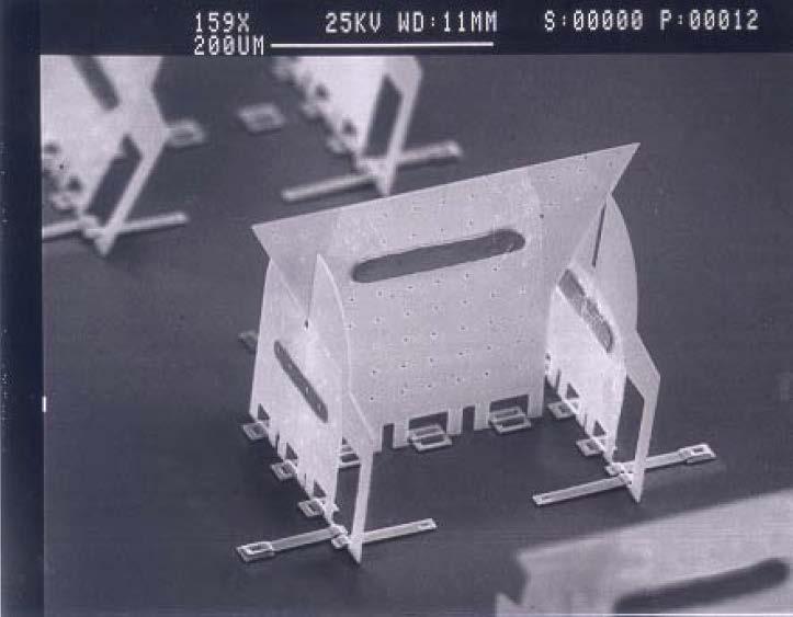
17 3D Assembly of Surface Micromachined Structures Surface micromachining usually generates planar structures (2D flaps). These 2D flaps could be moved out-of-plane using a number of methods to form 3D structures (micro assembly). Serial assembly: Piece by piece and device by device Using robot and micro manipulator (Zyvex) Low efficiency Parallel (self) assembly: Assembling all devices on substrate simultaneously Using integrated micro actuators High efficiency Configuration of the 2D flaps With micro hinges Without micro hinges


18 Micro Hinged Structures Etch hole The main flap can be rotated out of substrate surface around the hinge. Needs two structural layer and two sacrificial layer Rely on conformal deposition process


19 Self-assembly of Micro Hinged Structures Permalloy Wu, Proc. IEEE, 1997 Use magnetic force Use electrostatic force


20 Self-assembly of Planar Structures without Hinges Plastic Deformation Magnetic Assembly (PDMA) Magnetic material piece can be removed after PDMA.


21 Self-assembly of Planar Structures without Hinges Self-Assembly using surface tension force PR Solder Thermal stability is an issue. Syms, JMEMS, 2003
22 Self-assembly of Planar Structures without Hinges Self-Assembly using surface tension force


23 Surface Micromachining Foundry Process Multi-user MEMS Process 3 polysilicon surface micromachining process One process for different designs PolyMUMPS, SOIMUMPS, MetalMUMPS
24 Poly-MUMPS Examples
25 MUMPS Design Rules Overlapped region


26 Micro Motor Fabrication Process 2 nd Pass Si PSG Poly SiN


27 Micro Motor Fabrication Process 3 rd Pass Si PSG Poly SiN
Surface Micromachining
 Surface Micromachining Micro Actuators, Sensors, Systems Group University of Illinois at Urbana-Champaign Outline Definition of surface micromachining Most common surface micromachining materials - polysilicon
Surface micromachining and Process flow part 1
 Surface micromachining and Process flow part 1 Identify the basic steps of a generic surface micromachining process Identify the critical requirements needed to create a MEMS using surface micromachining
Regents of the University of California
 Surface-Micromachining Process Flow Photoresist Sacrificial Oxide Structural Polysilcon Deposit sacrificial PSG: Target = 2 m 1 hr. 40 min. LPCVD @450 o C Densify the PSG Anneal @950 o C for 30 min. Lithography
Lecture 10: MultiUser MEMS Process (MUMPS)
") MEMS: Fabrication Lecture 10: MultiUser MEMS Process (MUMPS) Prasanna S. Gandhi Assistant Professor, Department of Mechanical Engineering, Indian Institute of Technology, Bombay, 1 Recap Various VLSI based
MEMS: Fabrication Lecture 10: MultiUser MEMS Process (MUMPS) Prasanna S. Gandhi Assistant Professor, Department of Mechanical Engineering, Indian Institute of Technology, Bombay, 1 Recap Various VLSI based
EE C245 ME C218 Introduction to MEMS Design Fall 2011
 Lecture Outline EE C245 ME C218 Introduction to MEMS Design Fall 2011 Prof. Clark T.-C. Nguyen Dept. of Electrical Engineering & Computer Sciences University of California at Berkeley Berkeley, CA 94720
Regents of the University of California 1
 Electroplating: Metal MEMS Nickel Surface-Micromachining Process Flow Photoresist Wafer Release Etchant Use electroplating to obtain metal μstructures When thick: call it LIGA Pros: fast low temp deposition,
Lecture 5. SOI Micromachining. SOI MUMPs. SOI Micromachining. Silicon-on-Insulator Microstructures. Agenda:
 EEL6935 Advanced MEMS (Spring 2005) Instructor: Dr. Huikai Xie SOI Micromachining Agenda: SOI Micromachining SOI MUMPs Multi-level structures Lecture 5 Silicon-on-Insulator Microstructures Single-crystal
Today s Class. Materials for MEMS
 Lecture 2: VLSI-based Fabrication for MEMS: Fundamentals Prasanna S. Gandhi Assistant Professor, Department of Mechanical Engineering, Indian Institute of Technology, Bombay, Recap: Last Class What is
Regents of the University of California
 Topography Issues Degradation of lithographic resolution PR step coverage, streaking Thickness differences pose problems for reduction steppers Direction of Spin PR PR PR Stringers Problematic when using
Micro-Electro-Mechanical Systems (MEMS) Fabrication. Special Process Modules for MEMS. Principle of Sensing and Actuation
 Fabrication. Special Process Modules for MEMS. Principle of Sensing and Actuation") Micro-Electro-Mechanical Systems (MEMS) Fabrication Fabrication Considerations Stress-Strain, Thin-film Stress, Stiction Special Process Modules for MEMS Bonding, Cavity Sealing, Deep RIE, Spatial forming
Micro-Electro-Mechanical Systems (MEMS) Fabrication Fabrication Considerations Stress-Strain, Thin-film Stress, Stiction Special Process Modules for MEMS Bonding, Cavity Sealing, Deep RIE, Spatial forming
IC/MEMS Fabrication - Outline. Fabrication
 IC/MEMS Fabrication - Outline Fabrication overview Materials Wafer fabrication The Cycle: Deposition Lithography Etching Fabrication IC Fabrication Deposition Spin Casting PVD physical vapor deposition
4/10/2012. Introduction to Microfabrication. Fabrication
 Introduction to Microfabrication Fabrication 1 MEMS Fabrication Flow Basic Process Flow in Micromachining Nadim Maluf, An introduction to Microelectromechanical Systems Engineering 2 Thin Film Deposition
Mostafa Soliman, Ph.D. May 5 th 2014
 Mostafa Soliman, Ph.D. May 5 th 2014 Mostafa Soliman, Ph.D. 1 Basic MEMS Processes Front-End Processes Back-End Processes 2 Mostafa Soliman, Ph.D. Wafers Deposition Lithography Etch Chips 1- Si Substrate
Micro-Electro-Mechanical Systems (MEMS) Fabrication. Special Process Modules for MEMS. Principle of Sensing and Actuation
 Fabrication. Special Process Modules for MEMS. Principle of Sensing and Actuation") Micro-Electro-Mechanical Systems (MEMS) Fabrication Fabrication Considerations Stress-Strain, Thin-film Stress, Stiction Special Process Modules for MEMS Bonding, Cavity Sealing, Deep RIE, Spatial forming
Micro-Electro-Mechanical Systems (MEMS) Fabrication Fabrication Considerations Stress-Strain, Thin-film Stress, Stiction Special Process Modules for MEMS Bonding, Cavity Sealing, Deep RIE, Spatial forming
Solid State Sensors. Microfabrication 8/22/08 and 8/25/08
 Solid State Sensors Microfabrication 8/22/08 and 8/25/08 Purpose of This Material To introduce the student to microfabrication techniques as used to fabricate MEMS Sensors Understand concepts not specifics
Proceedings Post Fabrication Processing of Foundry MEMS Structures Exhibiting Large, Out-of-Plane Deflections
 Proceedings Post Fabrication Processing of Foundry MEMS Structures Exhibiting Large, Out-of-Plane Deflections LaVern Starman 1, *, John Walton 1, Harris Hall 1 and Robert Lake 2 1 Sensors Directorate,
Welcome MNT Conference 1 Albuquerque, NM - May 2010
 Welcome MNT Conference 1 Albuquerque, NM - May 2010 Introduction to Design Outline What is MEMs Design General Considerations Application Packaging Process Flow What s available Sandia SUMMiT Overview
EE C245 ME C218 Introduction to MEMS Design Fall 2007
 EE C245 ME C218 Introduction to MEMS Design Fall 2007 Prof. Clark T.-C. Nguyen Dept. of Electrical Engineering & Computer Sciences University of California at Berkeley Berkeley, CA 94720 Lecture 9: Surface
EE 5344 Introduction to MEMS. CHAPTER 3 Conventional Si Processing
 3. Conventional licon Processing Micromachining, Microfabrication. EE 5344 Introduction to MEMS CHAPTER 3 Conventional Processing Why silicon? Abundant, cheap, easy to process. licon planar Integrated
Cambridge University Press A Guide to Hands-on MEMS Design and Prototyping Joel A. Kubby Excerpt More information.
 1 Introduction 1.1 Overview of MEMS fabrication Microelectromechanical systems (MEMS) fabrication developed out of the thin-film processes first used for semiconductor fabrication. To understand the unique
EE C245 ME C218 Introduction to MEMS Design
 EE C245 ME C218 Introduction to MEMS Design Fall 2007 Prof. Clark T.-C. Nguyen Dept. of Electrical Engineering & Computer Sciences University of California at Berkeley Berkeley, CA 94720 Lecture 10: Surface
General Introduction to Microstructure Technology p. 1 What is Microstructure Technology? p. 1 From Microstructure Technology to Microsystems
 General Introduction to Microstructure Technology p. 1 What is Microstructure Technology? p. 1 From Microstructure Technology to Microsystems Technology p. 9 The Parallels to Microelectronics p. 15 The
Chapter 3 Silicon Device Fabrication Technology
 Chapter 3 Silicon Device Fabrication Technology Over 10 15 transistors (or 100,000 for every person in the world) are manufactured every year. VLSI (Very Large Scale Integration) ULSI (Ultra Large Scale
Micro-Electro-Mechanical Systems (MEMS) Fabrication. Special Process Modules for MEMS. Principle of Sensing and Actuation
 Fabrication. Special Process Modules for MEMS. Principle of Sensing and Actuation") Micro-Electro-Mechanical Systems (MEMS) Fabrication Fabrication Considerations Stress-Strain, Thin-film Stress, Stiction Special Process Modules for MEMS Bonding, Cavity Sealing, Deep RIE, Spatial forming
Micro-Electro-Mechanical Systems (MEMS) Fabrication Fabrication Considerations Stress-Strain, Thin-film Stress, Stiction Special Process Modules for MEMS Bonding, Cavity Sealing, Deep RIE, Spatial forming
FABRICATION PROCESSES FOR MAGNETIC MICROACTUATORS WITH POLYSILICON FLEXURES. Jack W. Judy and Richard S. Muller
 FABRICATION PROCESSES FOR MAGNETIC MICROACTUATORS WITH POLYSILICON FLEXURES Jack W. Judy and Richard S. Muller Berkeley Sensor & Actuator Center (BSAC) Department of EECS, University of California, Berkeley,
MEMS II: January 23. Lab 1: Pop-up mirror - PolyMUMPS - Thermal actuators - Mirror CoventorWare
 MEMS II: January 23 Lab 1: Pop-up mirror - PolyMUMPS - Thermal actuators - Mirror CoventorWare Microelectromechanical Systems (MEMS) Multi-User MEMS Processes (MUMPS) Example Design Anchor hole 2.0 0.5
Poly-SiGe MEMS actuators for adaptive optics
 Poly-SiGe MEMS actuators for adaptive optics Blake C.-Y. Lin a,b, Tsu-Jae King a, and Richard S. Muller a,b a Department of Electrical Engineering and Computer Sciences, b Berkeley Sensor and Actuator
The Physical Structure (NMOS)
") The Physical Structure (NMOS) Al SiO2 Field Oxide Gate oxide S n+ Polysilicon Gate Al SiO2 SiO2 D n+ L channel P Substrate Field Oxide contact Metal (S) n+ (G) L W n+ (D) Poly 1 3D Perspective 2 3 Fabrication
The Physical Structure (NMOS) Al SiO2 Field Oxide Gate oxide S n+ Polysilicon Gate Al SiO2 SiO2 D n+ L channel P Substrate Field Oxide contact Metal (S) n+ (G) L W n+ (D) Poly 1 3D Perspective 2 3 Fabrication
Fabrication Process. Crystal Growth Doping Deposition Patterning Lithography Oxidation Ion Implementation CONCORDIA VLSI DESIGN LAB
 Fabrication Process Crystal Growth Doping Deposition Patterning Lithography Oxidation Ion Implementation 1 Fabrication- CMOS Process Starting Material Preparation 1. Produce Metallurgical Grade Silicon
Surface Micromachining II
 Surface Micromachining II Dr. Thara Srinivasan Lecture 4 Picture credit: Sandia National Lab Lecture Outline Reading From reader: Bustillo, J. et al., Surface Micromachining of Microelectromechanical Systems,
Lecture #18 Fabrication OUTLINE
 Transistors on a Chip Lecture #18 Fabrication OUTLINE IC Fabrication Technology Introduction the task at hand Doping Oxidation Thin-film deposition Lithography Etch Lithography trends Plasma processing
PHYS 534 (Fall 2008) Process Integration OUTLINE. Examples of PROCESS FLOW SEQUENCES. >Surface-Micromachined Beam
 Process Integration OUTLINE. Examples of PROCESS FLOW SEQUENCES. >Surface-Micromachined Beam") PHYS 534 (Fall 2008) Process Integration Srikar Vengallatore, McGill University 1 OUTLINE Examples of PROCESS FLOW SEQUENCES >Semiconductor diode >Surface-Micromachined Beam Critical Issues in Process
PHYS 534 (Fall 2008) Process Integration Srikar Vengallatore, McGill University 1 OUTLINE Examples of PROCESS FLOW SEQUENCES >Semiconductor diode >Surface-Micromachined Beam Critical Issues in Process
Metallization deposition and etching. Material mainly taken from Campbell, UCCS
 Metallization deposition and etching Material mainly taken from Campbell, UCCS Application Metallization is back-end processing Metals used are aluminum and copper Mainly involves deposition and etching,
INF5490 RF MEMS. LN02: MEMS Fabrication. Spring 2012, Oddvar Søråsen Department of Informatics, UoO
 INF5490 RF MEMS LN02: MEMS Fabrication Spring 2012, Oddvar Søråsen Department of Informatics, UoO 1 Micromachining Today s lecture Important process steps General Summary: MEMS-specific steps Examples
SURFACE MICROMACHINING
 SURFACE MICROMACHINING Features are built up, layer by layer on the surface of a substrate. Surface micromachined devices are much smaller than bulk micromachined components. Nature of deposition process
PECVD SiO 2 SACRIFICIAL LAYERS FOR FABRICATION OF FREE - STANDING POLYSILICON FILAMENTS
 PECVD SiO 2 SACRIFICIAL LAYERS FOR FABRICATION OF FREE - STANDING POLYSILICON FILAMENTS Eliphas W. Simões 1, Rogério Furlan 2, Nilton I. Morimoto 3, Olivier Bonnaud 4*, Ana N. R. da Silva 5, Maria L. P.
Chapter 2 Manufacturing Process
 Digital Integrated Circuits A Design Perspective Chapter 2 Manufacturing Process 1 CMOS Process 2 CMOS Process (n-well) Both NMOS and PMOS must be built in the same silicon material. PMOS in n-well NMOS
EE 330 Lecture 9. IC Fabrication Technology Part II. -Oxidation -Epitaxy -Polysilicon -Planarization -Resistance and Capacitance in Interconnects
 EE 330 Lecture 9 IC Fabrication Technology Part II -Oxidation -Epitaxy -Polysilicon -Planarization -Resistance and Capacitance in Interconnects Review from Last Time Etching Dry etch (anisotropic) SiO
Chapter 4 Fabrication Process of Silicon Carrier and. Gold-Gold Thermocompression Bonding
 Chapter 4 Fabrication Process of Silicon Carrier and Gold-Gold Thermocompression Bonding 4.1 Introduction As mentioned in chapter 2, the MEMs carrier is designed to integrate the micro-machined inductor
Process Integration. MEMS Release Techniques Sacrificial Layer Removal Substrate Undercut
 Process Integration Self-aligned Techniques LOCOS- self-aligned channel stop Self-aligned Source/Drain Lightly Doped Drain (LDD) Self-aligned silicide (SALICIDE) Self-aligned oxide gap MEMS Release Techniques
Wireless implantable chip with integrated Nitinol-based pump for radio-controlled local drug delivery
 Electronic Supplementary Material (ESI) for Lab on a Chip. This journal is The Royal Society of Chemistry 2014 Electronic Supplementary Information Wireless implantable chip with integrated Nitinol-based
Chapter 2 OVERVIEW OF MEMS
 6 Chapter 2 OVERVIEW OF MEMS 2.1 MEMS and Microsystems The term MEMS is an abbreviation of microelectromechanical system. MEMS contains components ofsizes in 1 micrometer to 1 millimeter. The core element
Manufacturing Technologies for MEMS and SMART SENSORS
 4 Manufacturing Technologies for MEMS and SMART SENSORS Dr. H. K. Verma Distinguished Professor (EEE) Sharda University, Greater Noida (Formerly: Deputy Director and Professor of Instrumentation Indian
Lecture 7 CMOS MEMS. CMOS MEMS Processes. CMOS MEMS Processes. Why CMOS-MEMS? Agenda: CMOS MEMS: Fabrication. MEMS structures can be made
 EEL6935 Advanced MEMS (Spring 2005) Instructor: Dr. Huikai Xie CMOS MEMS Agenda: Lecture 7 CMOS MEMS: Fabrication Pre-CMOS Intra-CMOS Post-CMOS Deposition Etching Why CMOS-MEMS? Smart on-chip CMOS circuitry
Mikrosensorer. Microfabrication 1
 Mikrosensorer Microfabrication 1 Literature Introductory MEMS Fabrication and Applications Thomas M. Adams and Richard A. Layton Available as ebook on http://www.lub.lu.se/en/search/lubsearch.html This
EE C245 ME C218 Introduction to MEMS Design Fall 2007
 EE C245 ME C218 Introduction to MEMS Design Fall 2007 Prof. Clark T.-C. Nguyen Dept. of Electrical Engineering & Computer Sciences University of California at Berkeley Berkeley, CA 94720 Lecture 10: Bulk
CMOS Manufacturing process. Design rule set
 CMOS Manufacturing process Circuit design Set of optical masks Fabrication process Circuit designer Design rule set Process engineer All material: Chap. 2 of J. Rabaey, A. Chandrakasan, B. Nikolic, Digital
9/4/2008 GMU, ECE 680 Physical VLSI Design
 ECE680: Physical VLSI Design Chapter II CMOS Manufacturing Process 1 Dual-Well Trench-Isolated CMOS Process gate-oxide TiSi 2 AlCu Tungsten SiO 2 p-well poly n-well SiO 2 n+ p-epi p+ p+ 2 Schematic Layout
Lecture 6. Through-Wafer Interconnect. Agenda: Through-wafer Interconnect Polymer MEMS. Through-Wafer Interconnect -1. Through-Wafer Interconnect -2
 Agenda: EEL6935 Advanced MEMS (Spring 2005) Instructor: Dr. Huikai Xie Lecture 6 Through-wafer Interconnect EEL6935 Advanced MEMS 2005 H. Xie 1/21/2005 1 Motivations: Wafer-level packaging CMOS 3D Integration
Czochralski Crystal Growth
 Czochralski Crystal Growth Crystal Pulling Crystal Ingots Shaping and Polishing 300 mm wafer 1 2 Advantage of larger diameter wafers Wafer area larger Chip area larger 3 4 Large-Diameter Wafer Handling
Sensors and Actuators Designed and Fabricated in a. Micro-Electro-Mechanical-Systems (MEMS) Course. Using Standard MEMS Processes
 Course. Using Standard MEMS Processes") Sensors and Actuators Designed and Fabricated in a Micro-Electro-Mechanical-Systems (MEMS) Course Using Standard MEMS Processes M.G. Guvench University of Southern Maine guvench@maine.edu Abstract Use
Sensors and Actuators Designed and Fabricated in a Micro-Electro-Mechanical-Systems (MEMS) Course Using Standard MEMS Processes M.G. Guvench University of Southern Maine guvench@maine.edu Abstract Use
EE C247B ME C218 Introduction to MEMS Design Spring 2015
 EE C247B ME C218 Introduction to MEMS Design Spring 2015 Prof. Clark T.-C. Nguyen Dept. of Electrical Engineering & Computer Sciences University of California at Berkeley Berkeley, CA 94720 Lecture EE
EE C245 ME C218 Introduction to MEMS Design Fall 2011
 EE C245 ME C218 Introduction to MEMS Design Fall 2011 Prof. Clark T.-C. Nguyen Dept. of Electrical Engineering & Computer Sciences University of California at Berkeley Berkeley, CA 94720 Lecture EE C245:
EE C247B ME C218 Introduction to MEMS Design Spring 2014
 EE C247B ME C218 Introduction to MEMS Design Spring 2014 Prof. Clark T.-C. Nguyen Dept. of Electrical Engineering & Computer Sciences University of California at Berkeley Berkeley, CA 94720 Lecture EE
6.777J/2.732J Design and Fabrication of Microelectromechanical Devices Spring Term Solution to Problem Set 2 (16 pts)
") 6.777J/2.732J Design and Fabrication of Microelectromechanical Devices Spring Term 2007 By Brian Taff (Adapted from work by Feras Eid) Solution to Problem Set 2 (16 pts) Issued: Lecture 4 Due: Lecture
6.777J/2.732J Design and Fabrication of Microelectromechanical Devices Spring Term 2007 By Brian Taff (Adapted from work by Feras Eid) Solution to Problem Set 2 (16 pts) Issued: Lecture 4 Due: Lecture
Physical Vapor Deposition (PVD) Zheng Yang
 Zheng Yang") Physical Vapor Deposition (PVD) Zheng Yang ERF 3017, email: yangzhen@uic.edu Page 1 Major Fabrication Steps in MOS Process Flow UV light Mask oxygen Silicon dioxide photoresist exposed photoresist oxide
Physical Vapor Deposition (PVD) Zheng Yang ERF 3017, email: yangzhen@uic.edu Page 1 Major Fabrication Steps in MOS Process Flow UV light Mask oxygen Silicon dioxide photoresist exposed photoresist oxide
CS/ECE 5710/6710. N-type Transistor. N-type from the top. Diffusion Mask. Polysilicon Mask. CMOS Processing
 CS/ECE 5710/6710 CMOS Processing Addison-Wesley N-type Transistor D G +Vgs + Vds S N-type from the top i electrons - Diffusion Mask Mask for just the diffused regions Top view shows patterns that make
Chapter 3 CMOS processing technology
 Chapter 3 CMOS processing technology (How to make a CMOS?) Si + impurity acceptors(p-type) donors (n-type) p-type + n-type => pn junction (I-V) 3.1.1 (Wafer) Wafer = A disk of silicon (0.25 mm - 1 mm thick),
Micromachining AMT 2505
 Micromachining AMT 2505 Shanmuga Raja.B (BVB0912004) Module leader : Mr. Raja Hussain Introduction Micromachining are inherently connected to the evolution of Micro Electro Mechanical Systems (MEMS). Decades
Lecture 8-1 MCNC/MUMPS Process
 F. G. Tseng Fall/2016, 8-1, p1 Lecture 8-1 MCNC/MUMPS Process!! MCNC/MUMPS structure Layers provided: 7.0 µm Cr/Au=0.5 poly2=1.5 ox2=0.5 poly1=2.0 ox1=2.0 Poly0=0.5 Nitride=0.5 MUMPS Cross section with
MICROCHIP MANUFACTURING by S. Wolf
 MICROCHIP MANUFACTURING by S. Wolf Chapter 22 DRY-ETCHING for ULSI APPLICATIONS 2004 by LATTICE PRESS CHAPTER 22 - CONTENTS Types of Dry-Etching Processes The Physics & Chemistry of Plasma-Etching Etching
Process Integration. NMOS Generic NMOS Process Flow. CMOS - The MOSIS Process Flow
 Process Integration Self-aligned Techniques LOCOS- self-aligned channel stop Self-aligned Source/Drain Lightly Doped Drain (LDD) Self-aligned silicide (SALICIDE) Self-aligned oxide gap MEMS Release Techniques
EECS130 Integrated Circuit Devices
 EECS130 Integrated Circuit Devices Professor Ali Javey 9/13/2007 Fabrication Technology Lecture 1 Silicon Device Fabrication Technology Over 10 15 transistors (or 100,000 for every person in the world)
ECSE-6300 IC Fabrication Laboratory Lecture 4: Dielectrics and Poly-Si Deposition. Lecture Outline
 ECSE-6300 IC Fabrication Laboratory Lecture 4: Dielectrics and Poly-Si Deposition Prof. Rensselaer Polytechnic Institute Troy, NY 12180 Office: CII-6229 Tel.: (518) 276-2909 e-mails: luj@rpi.edu http://www.ecse.rpi.edu/courses/s18/ecse
Cristina Rusu Imego AB Cristina Rusu
 MEMS Fabrication Cristina Rusu Imego AB 2011-02-21 MEMS Semiconductors as mechanical materials Bulk micromachining Dry etching Wet etching Surface micromachining MUMPs Polymer MEMS Wafer bonding Technology:
Lect. 2: Basics of Si Technology
 Unit processes Thin Film Deposition Etching Ion Implantation Photolithography Chemical Mechanical Polishing 1. Thin Film Deposition Layer of materials ranging from fractions of nanometer to several micro-meters
CMOS Technology. Flow varies with process types & company. Start with substrate selection. N-Well CMOS Twin-Well CMOS STI
 CMOS Technology Flow varies with process types & company N-Well CMOS Twin-Well CMOS STI Start with substrate selection Type: n or p Doping level, resistivity Orientation, 100, or 101, etc Other parameters
4. Process Integration: Case Studies
 Case Study #2: FCantilevered Microgripper Surface Machined MEMS Case Study #2: FCantilevered Microgripper Sandia Lucent Sandia Integrated Accelerometers Optomechanical Systems Integrated Sensors 1 Bulk
Growth and Doping of SiC-Thin Films on Low-Stress, Amorphous Si 3 N 4 /Si Substrates for Robust Microelectromechanical Systems Applications
 Journal of ELECTRONIC MATERIALS, Vol. 31, No. 5, 2002 Special Issue Paper Growth and Doping of SiC-Thin Films on Low-Stress, Amorphous Si 3 N 4 /Si Substrates for Robust Microelectromechanical Systems
Manufacturing Process
 Digital Integrated Circuits A Design Perspective Jan M. Rabaey Anantha Chandrakasan Borivoje Nikolic Manufacturing Process July 30, 2002 1 CMOS Process 2 A Modern CMOS Process gate-oxide TiSi 2 AlCu Tungsten
Single crystal silicon supported thin film micromirrors for optical applications
 Single crystal silicon supported thin film micromirrors for optical applications Zhimin J. Yao* Noel C. MacDonald Cornell University School of Electrical Engineering and Cornell Nanofabrication Facility
MICRO-ELECTRO-MECHANICAL VARIABLE BLAZE GRATINGS
 MICRO-ELECTRO-MECHANICAL VARIABLE BLAZE GRATINGS D. M. Burns and V. M. Bright Air Force Institute of Technology Department of Electrical and Computer Engineering Wright-Patterson Air Force Base, OH 45433-7765
Review of CMOS Processing Technology
 - Scaling and Integration Moore s Law Unit processes Thin Film Deposition Etching Ion Implantation Photolithography Chemical Mechanical Polishing 1. Thin Film Deposition Layer of materials ranging from
ME 189 Microsystems Design and Manufacture. Chapter 9. Micromanufacturing
 ME 189 Microsystems Design and Manufacture Chapter 9 Micromanufacturing This chapter will offer an overview of the application of the various fabrication techniques described in Chapter 8 in the manufacturing
MEMS Fabrication. Beyond Integrated Circuits. MEMS Basic Concepts
 MEMS Fabrication Beyond Integrated Circuits MEMS Basic Concepts Uses integrated circuit fabrication techniques to make mechanical as well as electrical components on a single chip. Small size 1µm 1mm Typically
Introduction to CMOS VLSI Design. Layout, Fabrication, and Elementary Logic Design
 Introduction to CMOS VLSI Design Layout, Fabrication, and Elementary Logic Design CMOS Fabrication CMOS transistors are fabricated on silicon wafer Lithography process similar to printing press On each
ECE 659. Jan M. Rabaey Anantha Chandrakasan Borivoje Nikolic. July 30, Digital EE141 Integrated Circuits 2nd Manufacturing.
 Digital Integrated Circuits A Design Perspective Jan M. Rabaey Anantha Chandrakasan Borivoje Nikolic Manufacturing Process July 0, 00 1 CMOS Process 1 A Modern CMOS Process gate-oxide TiSi AlCu Tungsten
Microstructures using RF sputtered PSG film as a sacrificial layer in surface micromachining
 Sādhanā Vol. 34, Part 4, August 2009, pp. 557 562. Printed in India Microstructures using RF sputtered PSG film as a sacrificial layer in surface micromachining VIVEKANAND BHATT 1,, SUDHIR CHANDRA 1 and
Lecture 1A: Manufacturing& Layout
 Introduction to CMOS VLSI Design Lecture 1A: Manufacturing& Layout David Harris Harvey Mudd College Spring 2004 Steven Levitan Fall 2008 1 The Manufacturing Process For a great tour through the IC manufacturing
Preface Preface to First Edition
 Contents Foreword Preface Preface to First Edition xiii xv xix CHAPTER 1 MEMS: A Technology from Lilliput 1 The Promise of Technology 1 What Are MEMS or MST? 2 What Is Micromachining? 3 Applications and
Lecture 3: Integrated Processes
 Lecture 3: Integrated Processes Single-Crystal Silicon Process Integration Polysilicon Micromachining Process Integrated CMOS Micromachining Process ENE 5400, Spring 2004 1 Single Crystal Silicon ENE 5400,
Microfabrication of Integrated Circuits
 Microfabrication of Integrated Circuits OUTLINE History Basic Processes Implant; Oxidation; Photolithography; Masks Layout and Process Flow Device Cross Section Evolution Lecture 38, 12/05/05 Reading This
Complexity of IC Metallization. Early 21 st Century IC Technology
 EECS 42 Introduction to Digital Electronics Lecture # 25 Microfabrication Handout of This Lecture. Today: how are Integrated Circuits made? Silicon wafers Oxide formation by growth or deposition Other
Dr. Lynn Fuller Webpage:
 ROCHESTER INSTITUTE OF TECHNOLOGY MICROELECTRONIC ENGINEERING Microelectromechanical Systems (MEMs) Process Integration Dr. Lynn Fuller Webpage: http://people.rit.edu/lffeee 82 Lomb Memorial Drive Rochester,
Chemical Vapor Deposition
 Chemical Vapor Deposition ESS4810 Lecture Fall 2010 Introduction Chemical vapor deposition (CVD) forms thin films on the surface of a substrate by thermal decomposition and/or reaction of gas compounds
Lecture Day 2 Deposition
 Deposition Lecture Day 2 Deposition PVD - Physical Vapor Deposition E-beam Evaporation Thermal Evaporation (wire feed vs boat) Sputtering CVD - Chemical Vapor Deposition PECVD LPCVD MVD ALD MBE Plating
Micro-Scale Engineering I Microelectromechanical Systems (MEMS) Y. C. Lee
 Y. C. Lee") Micro-Scale Engineering I Microelectromechanical Systems (MEMS) Y. C. Lee Department of Mechanical Engineering University of Colorado Boulder, CO 80309-0427 leeyc@colorado.edu September 2, 2008 1 Three
Micro-Scale Engineering I Microelectromechanical Systems (MEMS) Y. C. Lee Department of Mechanical Engineering University of Colorado Boulder, CO 80309-0427 leeyc@colorado.edu September 2, 2008 1 Three
EE40 Lec 22. IC Fabrication Technology. Prof. Nathan Cheung 11/19/2009
 Suggested Reading EE40 Lec 22 IC Fabrication Technology Prof. Nathan Cheung 11/19/2009 300mm Fab Tour http://www-03.ibm.com/technology/manufacturing/technology_tour_300mm_foundry.html Overview of IC Technology
Polymer-based Microfabrication
 Polymer-based Microfabrication PDMS SU-8 PMMA Hydrogel 1 Soft Lithography Developed by Whitesides, et. al A set of techniques for microfabrication based on the use of lithography, soft substrate materials
A discussion of crystal growth, lithography, etching, doping, and device structures is presented in
 Chapter 5 PROCESSING OF DEVICES A discussion of crystal growth, lithography, etching, doping, and device structures is presented in the following overview gures. SEMICONDUCTOR DEVICE PROCESSING: AN OVERVIEW
Microstructure of Electronic Materials. Amorphous materials. Single-Crystal Material. Professor N Cheung, U.C. Berkeley
 Microstructure of Electronic Materials Amorphous materials Single-Crystal Material 1 The Si Atom The Si Crystal diamond structure High-performance semiconductor devices require defect-free crystals 2 Crystallographic
EE 330 Lecture 8. IC Fabrication Technology Part II. - Oxidation - Epitaxy - Polysilicon - Interconnects
 EE 330 Lecture 8 IC Fabrication Technology Part II - Oxidation - Epitaxy - Polysilicon - Interconnects Review from Last Time MOS Transistor Bulk Source Gate Drain p-channel MOSFET Lightly-doped n-type
EE 434 Lecture 9. IC Fabrication Technology
 EE 434 Lecture 9 IC Fabrication Technology Quiz 7 The layout of a film resistor with electrodes A and B is shown. If the sheet resistance of the film is 40 /, determine the resistance between nodes A and
Lecture 5: Micromachining
 MEMS: Fabrication Lecture 5: Micromachining Prasanna S. Gandhi Assistant Professor, Department of Mechanical Engineering, Indian Institute of Technology, Bombay, Recap: Last Class E-beam lithography X-ray
Manufacturing Process
 CMOS Manufacturing Process CMOS Process 1 A Modern CMOS Process gate-oxide TiSi AlCu Tungsten SiO n+ p-well p-epi poly n-well p+ SiO p+ Dual-Well Trench-Isolated CMOS Process Circuit Under Design V DD
Fabrication and Layout
 ECEN454 Digital Integrated Circuit Design Fabrication and Layout ECEN 454 3.1 A Glimpse at MOS Device Polysilicon Aluminum ECEN 475 4.2 1 Material Classification Insulators Glass, diamond, silicon oxide
FABRICATION OF CMOS INTEGRATED CIRCUITS. Dr. Mohammed M. Farag
 FABRICATION OF CMOS INTEGRATED CIRCUITS Dr. Mohammed M. Farag Outline Overview of CMOS Fabrication Processes The CMOS Fabrication Process Flow Design Rules EE 432 VLSI Modeling and Design 2 CMOS Fabrication
EE 330 Lecture 9. IC Fabrication Technology Part 2
 EE 330 Lecture 9 IC Fabrication Technology Part 2 Quiz 8 A 2m silicon crystal is cut into wafers using a wire saw. If the wire diameter is 220um and the wafer thickness is 350um, how many wafers will this
Lecture 19 Microfabrication 4/1/03 Prof. Andy Neureuther
 EECS 40 Spring 2003 Lecture 19 Microfabrication 4/1/03 Prof. ndy Neureuther How are Integrated Circuits made? Silicon wafers Oxide formation by growth or deposition Other films Pattern transfer by lithography
Microfabrication of Heterogeneous, Optimized Compliant Mechanisms SUNFEST 2001 Luo Chen Advisor: Professor G.K. Ananthasuresh
 Microfabrication of Heterogeneous, Optimized Compliant Mechanisms SUNFEST 2001 Luo Chen Advisor: Professor G.K. Ananthasuresh Fig. 1. Single-material Heatuator with selective doping on one arm (G.K. Ananthasuresh)