Latching Shape Memory Alloy Microactuator
|
|
|
- Blaise Sutton
- 5 years ago
- Views:
Transcription
1 Latching Shape Memory Alloy Microactuator ENMA490, Fall 00 S. Cabrera, N. Harrison, D. Lunking, R. Tang, C. Ziegler, T. Valentine
2 Outline Background Problem Project Development Design Evaluation Applications Device and Process Flow Summary/Future Research Materials Applications
3 Problem Statement Assignment: Develop a design for a microdevice, including materials choice and process sequence, that capitalizes on the properties of new materials. Survey: functional materials and MEMS Specific Device Goals: Actuates Uses Shape Memory Alloys Uses power only to switch states Concept: Latching shape-memory-alloy microactuator

4 Project Stimulus State of the Art: SMA microactuator Lai et al. The Characterization of TiNi Shape-Memory Actuated Microvalves. Mat. Res. Soc. Symp. Proc. 657, EE8.3.-EE8.3.6, 00. Uses SMA arms to raise and lower a Si island to seal the valve. Uses continuous Joule heating to keep valve open. TOP VIEW: Si island over valve SIDE VIEW: Joule heating NiTi SMA arm
5 Shape Memory Alloys Martensite-Austenite Transformation Cooling Applied Stress Applied Stress Re-heating Austenite Polydomain Martensite Single-domain Martensite Austenite Twinned domains (symmetric, inter-grown crystals)


6 Heat SMA valve opens SMA cools magnet keeps valve closed INITIAL DESIGN SMA cools valve stays open Heat SMA valve closes


7 Heat SMA valve closes SMA cools valve stays open FINAL DESIGN SMA cools magnet keeps valve closed Heat SMA valve opens
8 Cantilever Positions and Forces Based on beam theory Non-uniform shape change between SMA and substrate causes cantilever bending Thermal expansion causes bulk strain (α-α) T Martensite-austenite transformation creates lattice strain ε=-(a aust /a mart ) Ω =[(α-α) T] or [ε] ) 3 ( ) ( ) ( ) ( 6 t t t t t t E E b b t E b E t b t t t t E E b b k Ω + = kl d = 3 3 L EId F =
 NiTi (austenite) 83 6.6 0.305 http://www.keele.ac.uk/depts/ch/resources/xtal/classes.html, http://cst-www.nrl.navy.mil/ lattice/struk/b.html")
9 Material Properties Young s Modulus (GPa) Thermal Expansion Coefficient (*0-6 /K) Lattice Parameter (nm) Si N/A GaAs N/A NiTi (martensite) (smallest axis) NiTi (austenite) lattice/struk/b.html
10 Cantilever Positions and Forces Major assumptions: Can calculate martensite austenite strain from differing lattice constants Properties change linearly with austenite-martensite fraction during transformation Deflection Large effect from SMA, negligible effect (orders of magnitude less) from thermal expansion
11 Simulation
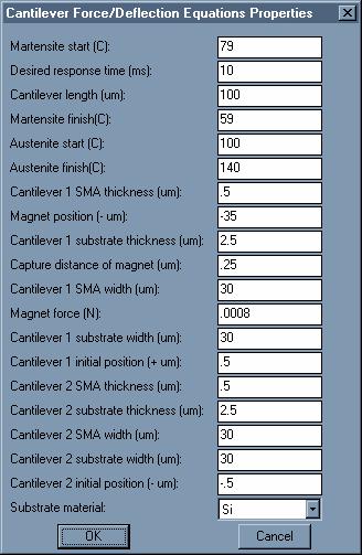
12 Simulation Deflection Results 00µm long, 30µm wide,.5µm thick substrate, 0.5µm thick SMA Tip deflection 39µm, Deflection <, Tip force 0.3mN Heat/cool cantilever : F() > F(magnet) > F() Heat/cool cantilever : F() > F(magnet) > F()
13 Tip Deflection Scaling E-0 Tip deflection (m).e-03.e-04.e-05.e-06 L 0.3L SMA thickness (um) Length (um) 0.03L
14 Process Flow (Single Cantilever) -Silicon wafer (green) with silicon dioxide (purple) grown or deposited on front and back surfaces. -Application of photoresist (orange), followed by exposure and development in UV (exposed areas indicated by green). -Buffered oxide etch removes exposed oxide layer. Oxide underneath unexposed photoresist remains. -Removal of photoresist in acetone/methanol is followed by KOH etch to remove exposed silicon until desired cantilever thickness is reached. -Deposition of NiTi (yellow) via sputtering, followed by 500C anneal under stress to train SMA film. -Deposition of magnetic material (blue) using a mask via sputtering on bottom of cantilever.
15 Process Flow (SMA Training) Small needles hold down cantilevers during post-deposition anneal Training process usually carried out at 500 C for 5 or more minutes Small green circles indicate needle placement with respect to cantilever wafer Thin film will remember its trained shape when it transforms to austenite Degree of actuation determined by deflection of cantilever during training process Side view of needle apparatus
16 Non-Latching Power Cycle Cumulative Energy Consumed (arb. units) Non-latching Duty Cycle Max energy usage Time Close d (%) Normally open Normally Closed Energy use based on time spent in secondary state. Energy = Power * Time Max energy used when 50% of time spent in secondary state. Above 50%, other type of actuator more efficient.
17 Latching Power Cycle Cumulative Energy consumed (arb. units) Latching Duty Cycles Switches (cycles * ) Low Power, Low Freq Low Power, High Freq Energy use based solely on number of switches. Energy = Energy per cycle * frequency of switching * time used Least energy used at low power to switch, low frequency of switching Low energy to switch, low frequency, latching is more energy efficient. High Power, Low Freq High Power, High Freq
18 Power Considerations Heat cantilevers to induce shape memory effect P = (m c T)/t = I R m - mass of cantilever, c - specific heat of cantilever, T - difference between A f and room temperature, t - desired response time Power differs slightly for martensite and austenite for constant I because of differing resistivity. From simulation: Required current = 0.7 ma Required power = W

19 Applications and Requirements Electrical Contacts Sensor Circuit breaker Optical Switching Telescope mirrors Gas/liquid Valves Drug release system outside world device TI thermal circuit breaker, Sandia pop-up mirror and drive system,
20 Summary Final design: dual cantilever system with SMA and magnetic materials to provide latching action Power consumption lower than that of a non-latching design when switching occurs infrequently and uses little energy Future work: Research magnetic material, packaging Specify application Continue analysis and optimization Build device
21 Backup
22 Shape Memory Effect Free-energy versus temperature curves for the parent (G p ) and martensite (G m ) structures in a shape memory alloy. From Otsuka (998), p.3, fig..7. Martensite-austenite phase transformation in shape memory alloys. From
23 Material Choice: NiTi SMA Near-equiatomic NiTi most widely used SMA today Property Transformation temperature Latent heat of transformation Melting point Specific heat Young s modulus Yield strength Value -00 to 0 C 5.78 cal/g 300 C 0.0 cal/g 83 GPa austenite; 8 to 4 GPa martensite 95 to 690 MPa austenite; 70 to 40 MPa martensite Ultimate tensile strength 895 MPa annealed; 900 MPa work-hardened % Elongation at failure 5 to 50% annealed; 5 to 0% work-hardened From

24 Nickel-Titanium Parent β (austenite) phase with B structure Martensite phase with monoclinic B9 structure B (cesium chloride) crystal structure. From lattice/struk/b.html B9 crystal structure. From Tang et al., p.3460, fig.5.

25
Shape Memory Alloys: Thermoelastic Martensite
 Shape Memory Alloys: Thermoelastic Martensite MatE 152 Thermoelastic Martensite Shape Memory Alloys (SMA) The strain of transformation is much less than the martensitic transformation in steel Thus product
Shape Memory Alloy Knowledge Evaluation Test. 1. What is the basic mechanism of the shape memory effect (SME)?
?") Shape Memory Alloy Knowledge Evaluation Test 1. What is the basic mechanism of the shape memory effect (SME)? a. Deformation due to the motion of mixed dislocations b. Interstitial diffusions within the
Shape Memory Alloy Knowledge Evaluation Test 1. What is the basic mechanism of the shape memory effect (SME)? a. Deformation due to the motion of mixed dislocations b. Interstitial diffusions within the
Thin film shape memory alloys for optical sensing applications
 Thin film shape memory alloys for optical sensing applications Y. Q. Fu, 1 J. K. Luo, 1,2 W.M. Huang, 3 A.J. Flewitt 1 and W.I. Milne 1 1 Department of Engineering, Cambridge University, 9 JJ Thomson Ave,
Micro-Electro-Mechanical Systems (MEMS) Fabrication. Special Process Modules for MEMS. Principle of Sensing and Actuation
 Fabrication. Special Process Modules for MEMS. Principle of Sensing and Actuation") Micro-Electro-Mechanical Systems (MEMS) Fabrication Fabrication Considerations Stress-Strain, Thin-film Stress, Stiction Special Process Modules for MEMS Bonding, Cavity Sealing, Deep RIE, Spatial forming
Micro-Electro-Mechanical Systems (MEMS) Fabrication Fabrication Considerations Stress-Strain, Thin-film Stress, Stiction Special Process Modules for MEMS Bonding, Cavity Sealing, Deep RIE, Spatial forming
Direct Measurement of the Nanoscale Mechanical Properties of NiTi Shape Memory Alloy
 Mat. Res. Soc. Symp. Proc. Vol. 791 2004 Materials Research Society Q7.11.1 Direct Measurement of the Nanoscale Mechanical Properties of NiTi Shape Memory Alloy Gordon A. Shaw 1, Wendy C. Crone 2 1 Department
Poly-SiGe MEMS actuators for adaptive optics
 Poly-SiGe MEMS actuators for adaptive optics Blake C.-Y. Lin a,b, Tsu-Jae King a, and Richard S. Muller a,b a Department of Electrical Engineering and Computer Sciences, b Berkeley Sensor and Actuator
Micro-Electro-Mechanical Systems (MEMS) Fabrication. Special Process Modules for MEMS. Principle of Sensing and Actuation
 Fabrication. Special Process Modules for MEMS. Principle of Sensing and Actuation") Micro-Electro-Mechanical Systems (MEMS) Fabrication Fabrication Considerations Stress-Strain, Thin-film Stress, Stiction Special Process Modules for MEMS Bonding, Cavity Sealing, Deep RIE, Spatial forming
Micro-Electro-Mechanical Systems (MEMS) Fabrication Fabrication Considerations Stress-Strain, Thin-film Stress, Stiction Special Process Modules for MEMS Bonding, Cavity Sealing, Deep RIE, Spatial forming
FABRICATION PROCESSES FOR MAGNETIC MICROACTUATORS WITH POLYSILICON FLEXURES. Jack W. Judy and Richard S. Muller
 FABRICATION PROCESSES FOR MAGNETIC MICROACTUATORS WITH POLYSILICON FLEXURES Jack W. Judy and Richard S. Muller Berkeley Sensor & Actuator Center (BSAC) Department of EECS, University of California, Berkeley,
FEA and Experimental Studies of Adaptive Composite Materials with SMA Wires
 FEA and Experimental Studies of Adaptive Composite Materials with SMA Wires K.Kanas, C.Lekakou and N.Vrellos Abstract This study comprises finite element simulations and experimental studies of the shape
4. Process Integration: Case Studies
 Case Study #2: FCantilevered Microgripper Surface Machined MEMS Case Study #2: FCantilevered Microgripper Sandia Lucent Sandia Integrated Accelerometers Optomechanical Systems Integrated Sensors 1 Bulk
Thomas M. Adams Richard A. Layton. Introductory MEMS. Fabrication and Applications. Springer
 Thomas M. Adams Richard A. Layton Introductory MEMS Fabrication and Applications Springer Contents Preface xiü Part I Fabrication Chapter 1: Introduction 3 1.1 What are MEMS? 3 1.2 Why MEMS? 4 1.2.1. Low
PHYS 534 (Fall 2008) Process Integration OUTLINE. Examples of PROCESS FLOW SEQUENCES. >Surface-Micromachined Beam
 Process Integration OUTLINE. Examples of PROCESS FLOW SEQUENCES. >Surface-Micromachined Beam") PHYS 534 (Fall 2008) Process Integration Srikar Vengallatore, McGill University 1 OUTLINE Examples of PROCESS FLOW SEQUENCES >Semiconductor diode >Surface-Micromachined Beam Critical Issues in Process
PHYS 534 (Fall 2008) Process Integration Srikar Vengallatore, McGill University 1 OUTLINE Examples of PROCESS FLOW SEQUENCES >Semiconductor diode >Surface-Micromachined Beam Critical Issues in Process
Micro-Electro-Mechanical Systems (MEMS) Fabrication. Special Process Modules for MEMS. Principle of Sensing and Actuation
 Fabrication. Special Process Modules for MEMS. Principle of Sensing and Actuation") Micro-Electro-Mechanical Systems (MEMS) Fabrication Fabrication Considerations Stress-Strain, Thin-film Stress, Stiction Special Process Modules for MEMS Bonding, Cavity Sealing, Deep RIE, Spatial forming
Micro-Electro-Mechanical Systems (MEMS) Fabrication Fabrication Considerations Stress-Strain, Thin-film Stress, Stiction Special Process Modules for MEMS Bonding, Cavity Sealing, Deep RIE, Spatial forming
Development and Verification of Sputtered Thin-Film Nickel-Titanium (NiTi) Shape Memory Alloy (SMA)
 Shape Memory Alloy (SMA)") ARL-TR-7364 AUG 2015 US Army Research Laboratory Development and Verification of Sputtered Thin-Film Nickel-Titanium (NiTi) Shape Memory Alloy (SMA) by Cory R Knick and Christopher J Morris Approved for
ARL-TR-7364 AUG 2015 US Army Research Laboratory Development and Verification of Sputtered Thin-Film Nickel-Titanium (NiTi) Shape Memory Alloy (SMA) by Cory R Knick and Christopher J Morris Approved for
Laser Annealing of Amorphous Ni-Ti Shape Memory Alloy Thin Films
 Laser Annealing of Amorphous Ni-Ti Shape Memory Alloy Thin Films Xi Wang, Zhenyu Xue, Joost J. Vlassak Division of Engineering and Applied Sciences, Harvard University, Cambridge, MA, U.S.A. Yves Bellouard
Chapter 3 CMOS processing technology
 Chapter 3 CMOS processing technology (How to make a CMOS?) Si + impurity acceptors(p-type) donors (n-type) p-type + n-type => pn junction (I-V) 3.1.1 (Wafer) Wafer = A disk of silicon (0.25 mm - 1 mm thick),
SMART VORTEX GENERATOR USING SHAPE MEMORY ALLOY
 25 TH INTERNATIONAL CONGRESS OF THE AERONAUTICAL SCIENCES SMART VORTEX GENERATOR USING SHAPE MEMORY ALLOY Tadashige Ikeda*, Shinya Masuda*, Takeshi Miyasaka**, Tetsuhiko Ueda* *Nagoya University, **Gifu
Welcome MNT Conference 1 Albuquerque, NM - May 2010
 Welcome MNT Conference 1 Albuquerque, NM - May 2010 Introduction to Design Outline What is MEMs Design General Considerations Application Packaging Process Flow What s available Sandia SUMMiT Overview
Investigation on thermo-mechanical behavior of shape memory alloy actuator
 ARCHIVES OF ELECTRICAL ENGINEERING VOL. 66(4), pp. 751-760 (2017) DOI 10.1515/aee-2017-0057 Investigation on thermo-mechanical behavior of shape memory alloy actuator MILENA KURZAWA, DOROTA STACHOWIAK
Module 6: Smart Materials & Smart Structural Control Lecture 34: Shape Memory Alloy based Actuators. The Lecture Contains: Shape Memory Alloy
 The Lecture Contains: Shape Memory Alloy Constitutive Relationship Tanaka Model file:///d /chitra/vibration_upload/lecture34/34_1.htm[6/25/2012 12:42:36 PM] Shape Memory Alloy (SMA) based Actuators Shape
Computer Simulation of Nanoparticle Aggregate Fracture
 Mater. Res. Soc. Symp. Proc. Vol. 1056 2008 Materials Research Society 1056-HH08-45 Computer Simulation of Nanoparticle Aggregate Fracture Takumi Hawa 1,2, Brian Henz 3, and Michael Zachariah 1,2 1 National
User Implemented Nitinol Material Model in ANSYS
 Abstract User Implemented Nitinol Material Model in ANSYS Peter R. Barrett, P.E. Computer Aided Engineering Associates, Inc. Daniel Fridline, Ph.D. Computer Aided Engineering Associates, Inc. Nitinol is
Iron Based Transforming Single Crystals Huseyin Sehitoglu, C. Efstathiou, H. J. Maier, Y. Chumlyakov
 Iron Based Transforming Single Crystals Huseyin Sehitoglu, C. Efstathiou, H. J. Maier, Y. Chumlyakov University of Illinois, Department of Mechanical and Industrial Engineering, Urbana, IL 61801 Presented
Microfabrication of Integrated Circuits
 Microfabrication of Integrated Circuits OUTLINE History Basic Processes Implant; Oxidation; Photolithography; Masks Layout and Process Flow Device Cross Section Evolution Lecture 38, 12/05/05 Reading This
Surface micromachining and Process flow part 1
 Surface micromachining and Process flow part 1 Identify the basic steps of a generic surface micromachining process Identify the critical requirements needed to create a MEMS using surface micromachining
Co-Evolution of Stress and Structure During Growth of Polycrystalline Thin Films
 Co-Evolution of Stress and Structure During Growth of Polycrystalline Thin Films Carl V. Thompson and Hang Z. Yu* Dept. of Materials Science and Engineering MIT, Cambridge, MA, USA Effects of intrinsic
Lecture 19 Microfabrication 4/1/03 Prof. Andy Neureuther
 EECS 40 Spring 2003 Lecture 19 Microfabrication 4/1/03 Prof. ndy Neureuther How are Integrated Circuits made? Silicon wafers Oxide formation by growth or deposition Other films Pattern transfer by lithography
Shape Memory Alloys and its Application in MEMS Devices
 Research Article International Journal of Current Engineering and Technology ISSN 2277-4106 2013 INPRESSCO. All Rights Reserved. Available at http://inpressco.com/category/ijcet Shape Memory Alloys and
MEMS II: January 23. Lab 1: Pop-up mirror - PolyMUMPS - Thermal actuators - Mirror CoventorWare
 MEMS II: January 23 Lab 1: Pop-up mirror - PolyMUMPS - Thermal actuators - Mirror CoventorWare Microelectromechanical Systems (MEMS) Multi-User MEMS Processes (MUMPS) Example Design Anchor hole 2.0 0.5
THE ANALYSIS OF STRESS DISTRIBUTION BASED ON MEASUREMENTS USING TWO METHODS OF X-RAY APPLICATION
 182 THE ANALYSIS OF STRESS DISTRIBUTION BASED ON MEASUREMENTS USING TWO METHODS OF X-RAY APPLICATION ABSTRACT Barbara Kucharska Institute of Materials Engineering, Czestochowa University of Technology,
Progress in Monolithic III-V/Si and towards processing III-V Devices in Silicon Manufacturing. E.A. (Gene) Fitzgerald
 Fitzgerald") Progress in Monolithic III-V/Si and towards processing III-V Devices in Silicon Manufacturing E.A. (Gene) Fitzgerald M.J. Mori, C.L.Dohrman, K. Chilukuri MIT Cambridge, MA USA Funding: MARCO IFC and Army
Progress in Monolithic III-V/Si and towards processing III-V Devices in Silicon Manufacturing E.A. (Gene) Fitzgerald M.J. Mori, C.L.Dohrman, K. Chilukuri MIT Cambridge, MA USA Funding: MARCO IFC and Army
Schematic creation of MOS field effect transistor.
 Schematic creation of MOS field effect transistor. Gate electrode Drain electrode Source electrode Gate oxide Gate length Page 1 Step 0 The positively doped silicon wafer is first coated with an insulating
From actuation control to ferromagnetism and biocompatibility in shape memory alloys
 EUROPEAN UNION GOVERNMENT OF ROMANIA SERBIAN GOVERNMENT Structural Funds 2007-2013 Romania Republic of Serbia IPA Cross-border Cooperation Programme From actuation control to ferromagnetism and biocompatibility
Complexity of IC Metallization. Early 21 st Century IC Technology
 EECS 42 Introduction to Digital Electronics Lecture # 25 Microfabrication Handout of This Lecture. Today: how are Integrated Circuits made? Silicon wafers Oxide formation by growth or deposition Other
ATI 201 HP /ATI 201L HP
 Stainless Steel: Austenitic (UNS S20100 and S20103) GENERAL PROPERTIES and L austenitic stainless steels belong to the 200 series of Cr-Mn-Ni stainless alloys, which are similar to the 300 series of Cr-Ni
Fabrication and Characterization of Fe-Pd Ferromagnetic Shape-Memory Thin Films
 Mat. Res. Soc. Symp. Proc. Vol. 785 24 Materials Research Society D7.4.1 Fabrication and Characterization of Fe-Pd Ferromagnetic Shape-Memory Thin Films Yuki Sugimura, Tzahi Cohen-Karni, Patrick McCluskey
EXCIMER LASER ANNEALING FOR LOW- TEMPERATURE POLYSILICON THIN FILM TRANSISTOR FABRICATION ON PLASTIC SUBSTRATES
 EXCIMER LASER ANNEALING FOR LOW- TEMPERATURE POLYSILICON THIN FILM TRANSISTOR FABRICATION ON PLASTIC SUBSTRATES G. Fortunato, A. Pecora, L. Maiolo, M. Cuscunà, D. Simeone, A. Minotti, and L. Mariucci CNR-IMM,
Today s Class. Materials for MEMS
 Lecture 2: VLSI-based Fabrication for MEMS: Fundamentals Prasanna S. Gandhi Assistant Professor, Department of Mechanical Engineering, Indian Institute of Technology, Bombay, Recap: Last Class What is
Doping and Oxidation
 Technische Universität Graz Institute of Solid State Physics Doping and Oxidation Franssila: Chapters 13,14, 15 Peter Hadley Technische Universität Graz Institute of Solid State Physics Doping Add donors
NANOINDENTATION OF SILICON CARBIDE WAFER COATINGS
 NANOINDENTATION OF SILICON CARBIDE WAFER COATINGS Prepared by Jesse Angle 6 Morgan, Ste156, Irvine CA 9618 P: 949.461.99 F: 949.461.93 nanovea.com Today's standard for tomorrow's materials. 010 NANOVEA
SECTION A. NATURAL SCIENCES TRIPOS Part IA. Friday 4 June to 4.30 MATERIALS AND MINERAL SCIENCES
 NATURAL SCIENCES TRIPOS Part IA Friday 4 June 1999 1.30 to 4.30 MATERIALS AND MINERAL SCIENCES Answer five questions; two from each of sections A and B and one from section C. Begin each answer at the
EE 330 Lecture 9. IC Fabrication Technology Part 2
 EE 330 Lecture 9 IC Fabrication Technology Part 2 Quiz 8 A 2m silicon crystal is cut into wafers using a wire saw. If the wire diameter is 220um and the wafer thickness is 350um, how many wafers will this
MEASUREMENTS OF MECHANICAL PROPERTIES OF MICROFABRICATED THIN FILMS
 MEASUREMENTS OF MECHANCAL PROPERTES OF MCROFABRCATED THN FLMS H. Ogawa, K. Suzuki**, S. Kaneko", Y. Nakano**, Y. shikawa and T. Kitahara Mechanical Engineering Laboratory, AST, MT, Department of Advanced
EE 330 Lecture 8. IC Fabrication Technology Part II. - Masking - Photolithography - Deposition - Etching - Diffusion
 EE 330 Lecture 8 IC Fabrication Technology Part II?? - Masking - Photolithography - Deposition - Etching - Diffusion Review from Last Time Technology Files Provide Information About Process Process Flow
My Experience with Ti Ni-Based and Ti-Based Shape Memory Alloys
 Shap. Mem. Superelasticity (2017) 3:279 314 https://doi.org/10.1007/s40830-017-0122-3 SPECIAL ISSUE: A TRIBUTE TO PROF. SHUICHI MIYAZAKI FROM FUNDAMENTALS TO APPLICATIONS, INVITED REVIEW PAPER My Experience
Thin film shape memory composites
 Thin film shape memory composites Bernhard Winzek, Tobias Sterzl, Holger Rumpf, Nikolai Botkin, Eckhard Quandt center of advanced european studies and research (caesar), Bonn, Germany Introduction Thin
Lecture 5. SOI Micromachining. SOI MUMPs. SOI Micromachining. Silicon-on-Insulator Microstructures. Agenda:
 EEL6935 Advanced MEMS (Spring 2005) Instructor: Dr. Huikai Xie SOI Micromachining Agenda: SOI Micromachining SOI MUMPs Multi-level structures Lecture 5 Silicon-on-Insulator Microstructures Single-crystal
On the lower thickness boundary of sputtered TiNi films for shape memory application
 Thin Solid Films 515 (26) 8 86 www.elsevier.com/locate/tsf On the lower thickness boundary of sputtered TiNi films for shape memory application Y.Q. Fu a,b, *, Sam Zhang b, M.J. Wu b, W.M. Huang b, H.J.
35 Hz shape memory alloy actuator with bending-twisting
 Supplementary Information 35 Hz shape memory alloy actuator with bending-twisting mode Sung-Hyuk Song 1, Jang-Yeob Lee 1, Hugo Rodrigue 1, Ik-Seong Choi 1, Yeon June Kang 1, and Sung-Hoon Ahn 1,2,* 1 Department
Growth and Doping of SiC-Thin Films on Low-Stress, Amorphous Si 3 N 4 /Si Substrates for Robust Microelectromechanical Systems Applications
 Journal of ELECTRONIC MATERIALS, Vol. 31, No. 5, 2002 Special Issue Paper Growth and Doping of SiC-Thin Films on Low-Stress, Amorphous Si 3 N 4 /Si Substrates for Robust Microelectromechanical Systems
This Appendix discusses the main IC fabrication processes.
 IC Fabrication B B.1 Introduction This Appendix discusses the main IC fabrication processes. B.2 NMOS fabrication NMOS transistors are formed in a p-type substrate. The NMOS fabrication process requires
EE 330 Lecture 8. IC Fabrication Technology Part II. - Oxidation - Epitaxy - Polysilicon - Interconnects
 EE 330 Lecture 8 IC Fabrication Technology Part II - Oxidation - Epitaxy - Polysilicon - Interconnects Review from Last Time MOS Transistor Bulk Source Gate Drain p-channel MOSFET Lightly-doped n-type
Actuator 3 Piezoelectric and shape memory alloy technology
 Actuator 3 Piezoelectric and shape memory alloy technology ME490A Dr. C. Alex Simpkins SDSU Dept. of Mechanical Engineering Adapted from a presentaeon by Dr. Kee Moon Piezoelectric property Direct piezoelectric
Experimental Evaluation of Shape Memory Alloy Characteristics
 International Journal of Computing Academic Research (IJCAR) ISSN 2305-9184, Volume 6, Number 3 (June 2017), pp.92-100 MEACSE Publications http://www.meacse.org/ijcar Experimental Evaluation of Shape Memory
Characterization and 3-D Modeling of Ni60Ti SMA for Actuation of a Variable Geometry Jet Engine Chevron
 Characterization and 3-D Modeling of Ni60Ti SMA for Actuation of a Variable Geometry Jet Engine Chevron Darren Hartl Dimitris Lagoudas Texas A&M University SPIE Smart Structures and Materials/NDE Conference
Process Flow in Cross Sections
 Process Flow in Cross Sections Process (simplified) 0. Clean wafer in nasty acids (HF, HNO 3, H 2 SO 4,...) --> wear gloves! 1. Grow 500 nm of SiO 2 (by putting the wafer in a furnace with O 2 2. Coat
High Entropy Shape Memory Alloys (HESMA) Alloy Compositions, Processing and Microstructures
 Alloy Compositions, Processing and Microstructures") High Entropy Shape Memory Alloys (HESMA) Alloy Compositions, Processing and Microstructures David Piorunek, Jan Frenzel, Gunther Eggeler EG 101/32-1 Outline Shape memory alloys & martensitic transformation
High Entropy Shape Memory Alloys (HESMA) Alloy Compositions, Processing and Microstructures David Piorunek, Jan Frenzel, Gunther Eggeler EG 101/32-1 Outline Shape memory alloys & martensitic transformation
Chapter 2 OVERVIEW OF MEMS
 6 Chapter 2 OVERVIEW OF MEMS 2.1 MEMS and Microsystems The term MEMS is an abbreviation of microelectromechanical system. MEMS contains components ofsizes in 1 micrometer to 1 millimeter. The core element
NANOINDENTATION OF ANNEALED AND AS-SPUTTERED THIN FILMS OF NICKEL TITANIUM SHAPE MEMORY ALLOYS
 NANOINDENTATION OF ANNEALED AND AS-SPUTTERED THIN FILMS OF NICKEL TITANIUM SHAPE MEMORY ALLOYS A Thesis presented to the Faculty of California Polytechnic State University, San Luis Obispo In Partial Fulfillment
EE40 Lec 22. IC Fabrication Technology. Prof. Nathan Cheung 11/19/2009
 Suggested Reading EE40 Lec 22 IC Fabrication Technology Prof. Nathan Cheung 11/19/2009 300mm Fab Tour http://www-03.ibm.com/technology/manufacturing/technology_tour_300mm_foundry.html Overview of IC Technology
Stainless Steel (17/4PH&630) Bar
 Bar") SPECIFICATIONS Commercial 17/4 PH EN 1.4542 Precipitation hardening stainless steels are chromium and nickel containing steels that provide an optimum combination of the properties of martensitic and austenitic
SPECIFICATIONS Commercial 17/4 PH EN 1.4542 Precipitation hardening stainless steels are chromium and nickel containing steels that provide an optimum combination of the properties of martensitic and austenitic
Shape Recovery after Nanoindentation of NiTi Thin Films
 Shape Recovery after Nanoindentation of NiTi Thin Films W. C. Crone *, G.A. Shaw œ, D. S. Stone, A. D. Johnson φ, A.B. Ellis œ Department of Engineering Physics, œ Department of Chemistry, Department of
SiGeC Cantilever Micro Cooler
 Mat. Res. Soc. Symp. Proc. Vol. 793 2004 Materials Research Society S11.3.1 SiGeC Cantilever Micro Cooler Gehong Zeng, Ali Shakouri 1 *, Edward Croke 2, Yan Zhang 1, James Christofferson 1 and John E.
ATI 601 ATI 601. Technical Data Sheet. Nickel-base Alloy INTRODUCTION PRODUCT FORMS SPECIFICATIONS & CERTIFICATES (UNS N06601)
") Nickel-base Alloy (UNS N06601) INTRODUCTION alloy (UNS Designation N06601) is an austenitic nickel-chromium-iron alloy designed for both heat and corrosion resistance. As compared to ATI 600 alloy (UNS
Nickel-base Alloy (UNS N06601) INTRODUCTION alloy (UNS Designation N06601) is an austenitic nickel-chromium-iron alloy designed for both heat and corrosion resistance. As compared to ATI 600 alloy (UNS
Microfabrication of Heterogeneous, Optimized Compliant Mechanisms SUNFEST 2001 Luo Chen Advisor: Professor G.K. Ananthasuresh
 Microfabrication of Heterogeneous, Optimized Compliant Mechanisms SUNFEST 2001 Luo Chen Advisor: Professor G.K. Ananthasuresh Fig. 1. Single-material Heatuator with selective doping on one arm (G.K. Ananthasuresh)
Fabrication and Layout
 ECEN454 Digital Integrated Circuit Design Fabrication and Layout ECEN 454 3.1 A Glimpse at MOS Device Polysilicon Aluminum ECEN 475 4.2 1 Material Classification Insulators Glass, diamond, silicon oxide
Your Supplier for Fused Silica
 Your Supplier for Fused Silica Characteristics Our Company successfully developed synthetic fused silica SK-1300 as a result of significant improvements made by the conventional VAD (vapor-phase axial
Stainless Steel Bar
 SPECIFICATIONS Commercial 17/4 PH EN 1.4542 Precipitation hardening stainless steels are chromium and nickel containing steels that provide an optimum combination of the properties of martensitic and austenitic
DYNAMIC CONTROL OF PLATE WITH EMBEDDED SHAPE MEMORY ALLOY WIRES
 27 TH INTERNATIONAL CONGRESS OF THE AERONAUTICAL SCIENCES DYNAMIC CONTROL OF PLATE WITH EMBEDDED SHAPE MEMORY ALLOY WIRES F. Hedayati Dezfuli, S. Khalilian, A. Abedian Keywords: shape memory alloys, natural
Amorphous and Polycrystalline Thin-Film Transistors
 Part I Amorphous and Polycrystalline Thin-Film Transistors HYBRID AMORPHOUS AND POLYCRYSTALLINE SILICON DEVICES FOR LARGE-AREA ELECTRONICS P. Mei, J. B. Boyce, D. K. Fork, G. Anderson, J. Ho, J. Lu, Xerox
Effects of Film Thickness on the Yielding Behavior of Polycrystalline Gold Films
 Effects of Film Thickness on the Yielding Behavior of Polycrystalline Gold Films H.D. Espinosa and B.C. Prorok Department of Mechanical Engineering, Northwestern University Evanston, IL 628-3111, USA ABSTRACT
Fabrication Technology
 Fabrication Technology By B.G.Balagangadhar Department of Electronics and Communication Ghousia College of Engineering, Ramanagaram 1 OUTLINE Introduction Why Silicon The purity of Silicon Czochralski
R Sensor resistance (Ω) ρ Specific resistivity of bulk Silicon (Ω cm) d Diameter of measuring point (cm)
 ρ Specific resistivity of bulk Silicon (Ω cm) d Diameter of measuring point (cm)") 4 Silicon Temperature Sensors 4.1 Introduction The KTY temperature sensor developed by Infineon Technologies is based on the principle of the Spreading Resistance. The expression Spreading Resistance derives
4 Silicon Temperature Sensors 4.1 Introduction The KTY temperature sensor developed by Infineon Technologies is based on the principle of the Spreading Resistance. The expression Spreading Resistance derives
Evaluation of Young s modulus of thin coated layer on cold-rolled steel sheet
 Evaluation of Young s modulus of thin coated layer on cold-rolled steel sheet Hideyuki Kuwahara *1, Tetsuya Yamamoto 2 and Masayoshi Akiyama 3 1 MPT, Fukakusa, Fushimi-ku, Kyoto 612-8431, Japan 2 Canon
A DISLOCATION MODEL FOR THE PLASTIC DEFORMATION OF FCC METALS AN ANALYSIS OF PURE COPPER AND AUSTENITIC STEEL
 A DISLOCATION MODEL FOR THE PLASTIC DEFORMATION OF FCC METALS AN ANALYSIS OF PURE COPPER AND AUSTENITIC STEEL Background In the bcc model for work hardening in single phase materials, see (6), it is assumed
EE 330 Lecture 9. IC Fabrication Technology Part II. -Oxidation -Epitaxy -Polysilicon -Planarization -Resistance and Capacitance in Interconnects
 EE 330 Lecture 9 IC Fabrication Technology Part II -Oxidation -Epitaxy -Polysilicon -Planarization -Resistance and Capacitance in Interconnects Review from Last Time IC Fabrication Technology Crystal Preparation
Mechanical Hysteresis in Single Crystal Shape Memory Alloys
 Mechanical Hysteresis in Single Crystal Shape Memory Alloys R. F. Hamilton, H. Sehitoglu, C. Efstathiou Y. Chumlyakov 1, H. J. Maier 2 University of Illinois, Department of Mechanical and Industrial Engineering,
Deployable Soft Composite Structures
 Supplementary Information Deployable Soft Composite Structures Wei Wang 1, Hugo Rodrigue 1,2 and Sung-Hoon Ahn 1,2, 1 Department of Mechanical and Aerospace Engineering, Seoul National University, Seoul,
EOS NickelAlloy IN718 for EOSINT M 270 Systems
 EOS NickelAlloy IN718 for EOSINT M 270 Systems A number of different materials are available for use with EOSINT M systems, offering a broad range of e-manufacturing applications. EOS NickelAlloy IN718
Instructor: Dr. M. Razaghi. Silicon Oxidation
 SILICON OXIDATION Silicon Oxidation Many different kinds of thin films are used to fabricate discrete devices and integrated circuits. Including: Thermal oxides Dielectric layers Polycrystalline silicon
Bulk Silicon Micromachining
 Bulk Silicon Micromachining Micro Actuators, Sensors, Systems Group University of Illinois at Urbana-Champaign Outline Types of bulk micromachining silicon anisotropic etching crystal orientation isotropic
ATI 418 SPL alloy is readily forgeable and has fair machinability and cold formability in the annealed condition.
 ATI 418 SPL Stainless Steel (UNS S41800) GENERAL PROPERTIES ATI 418 SPL alloy (Greek Ascoloy) is a corrosion and heat resistant stainless steel similar in many respects to Type 410 but exhibiting improved
5.8 Diaphragm Uniaxial Optical Accelerometer
 5.8 Diaphragm Uniaxial Optical Accelerometer Optical accelerometers are based on the BESOI (Bond and Etch back Silicon On Insulator) wafers, supplied by Shin-Etsu with (100) orientation, 4 diameter and
Because of equipment availability, cost, and time, we will use aluminum as the top side conductor
 Because of equipment availability, cost, and time, we will use aluminum as the top side conductor Top Side Conductor vacuum deposition Aluminum sputter deposit in Argon plasma CVC 601-sputter deposition
Preprint - Mechatronics 2008, Le Grand-Bornand, France, May
 Potentialities of piezoresistive cantilever force sensors based on free standing thick films Hélène Debéda(*), Isabelle Dufour, Patrick Ginet, Claude Lucat University of Bordeaux 1, IMS Laboratory, 51
Problem 1 Lab Questions ( 20 points total)
") Problem 1 Lab Questions ( 20 points total) (a) (3 points ) In our EE143 lab, we use Phosphorus for the source and drain diffusion. However, most advanced processes use Arsenic. What is the advantage of
Problem 1 Lab Questions ( 20 points total) (a) (3 points ) In our EE143 lab, we use Phosphorus for the source and drain diffusion. However, most advanced processes use Arsenic. What is the advantage of
micro resist technology
 Characteristics Processing guidelines Negative Tone Photoresist Series ma-n 2400 ma-n 2400 is a negative tone photoresist series designed for the use in micro- and nanoelectronics. The resists are available
CS/ECE 5710/6710. N-type Transistor. N-type from the top. Diffusion Mask. Polysilicon Mask. CMOS Processing
 CS/ECE 5710/6710 CMOS Processing Addison-Wesley N-type Transistor D G +Vgs + Vds S N-type from the top i electrons - Diffusion Mask Mask for just the diffused regions Top view shows patterns that make
Mechanical Limitations of Materials for Steel Foil Based Flexible Electronics
 Mater. Res. Soc. Symp. Proc. Vol. 30 2008 Materials Research Society 30-G03-14 Mechanical Limitations of Materials for Steel Foil Based Flexible Electronics Po-Chin Kuo 1, Vasilios G. Chouvardas 2, Jeff
Micro-Scale Engineering I Microelectromechanical Systems (MEMS) Y. C. Lee
 Y. C. Lee") Micro-Scale Engineering I Microelectromechanical Systems (MEMS) Y. C. Lee Department of Mechanical Engineering University of Colorado Boulder, CO 80309-0427 leeyc@colorado.edu September 2, 2008 1 Three
Micro-Scale Engineering I Microelectromechanical Systems (MEMS) Y. C. Lee Department of Mechanical Engineering University of Colorado Boulder, CO 80309-0427 leeyc@colorado.edu September 2, 2008 1 Three
Stainless Steel (17/4PH&630) Bar
 Bar") SPECIFICATIONS Commercial 17/4 PH EN 1.4542 Precipitation hardening stainless steels are chromium and nickel containing steels that provide an optimum combination of the properties of martensitic and austenitic
SPECIFICATIONS Commercial 17/4 PH EN 1.4542 Precipitation hardening stainless steels are chromium and nickel containing steels that provide an optimum combination of the properties of martensitic and austenitic
Introduction to Lithography
 Introduction to Lithography G. D. Hutcheson, et al., Scientific American, 290, 76 (2004). Moore s Law Intel Co-Founder Gordon E. Moore Cramming More Components Onto Integrated Circuits Author: Gordon E.
General Introduction to Microstructure Technology p. 1 What is Microstructure Technology? p. 1 From Microstructure Technology to Microsystems
 General Introduction to Microstructure Technology p. 1 What is Microstructure Technology? p. 1 From Microstructure Technology to Microsystems Technology p. 9 The Parallels to Microelectronics p. 15 The
Deposition and characterization of sputtered ZnO films
 Superlattices and Microstructures 42 (2007) 89 93 www.elsevier.com/locate/superlattices Deposition and characterization of sputtered ZnO films W.L. Dang, Y.Q. Fu, J.K. Luo, A.J. Flewitt, W.I. Milne Electrical
MOSFET. n+ poly Si. p- substrate
 EE143 Midterm #1 Solutions Fall 2005 (maximum score is 97) Problem 1 Processing Modules and Simple Process Sequence (25 points total) The following schematic cross-section shows a MOSFET together with
The ATI 17-4 precipitation hardening stainless steel (S17400) is covered by the following wrought product specifications.
 is covered by the following wrought product specifications.") ATI 17-4 Precipitation Hardening Stainless Steel (UNS S17400) INTRODUCTION ATI 17-4 precipitation hardening stainless steel (S17400), Type 630, is a chromium-nickel-copper precipitation hardening stainless
ATI 17-4 Precipitation Hardening Stainless Steel (UNS S17400) INTRODUCTION ATI 17-4 precipitation hardening stainless steel (S17400), Type 630, is a chromium-nickel-copper precipitation hardening stainless
Structural changes of polycrystalline silicon layers during high temperature annealing
 Structural changes of polycrystalline silicon layers during high temperature annealing D. Lysáček, L. Válek ON SEMICONDUCTOR CZECH REPUBLIC, Rožnov p. R., david.lysacek@onsemi.com Abstract The structure
Stainless Steel (17/4PH&630) Bar
 Bar") SPECIFICATIONS Commercial 17/4 PH EN 1.4542 Precipitation hardening stainless steels are chromium and nickel containing steels that provide an optimum combination of the properties of martensitic and austenitic
SPECIFICATIONS Commercial 17/4 PH EN 1.4542 Precipitation hardening stainless steels are chromium and nickel containing steels that provide an optimum combination of the properties of martensitic and austenitic
Deforming films of active materials: new concepts for producing motion at small scales (using applied fields)
") Deforming films of active materials: new concepts for producing motion at small scales (using applied fields) Richard D. James University of Minnesota james@umn.edu COLLABORATIONS, POSTDOCS, STUDENTS Chris
Deforming films of active materials: new concepts for producing motion at small scales (using applied fields) Richard D. James University of Minnesota james@umn.edu COLLABORATIONS, POSTDOCS, STUDENTS Chris
VLSI INTRODUCTION P.VIDYA SAGAR ( ASSOCIATE PROFESSOR) Department of Electronics and Communication Engineering, VBIT
 Department of Electronics and Communication Engineering, VBIT") VLSI INTRODUCTION P.VIDYA SAGAR ( ASSOCIATE PROFESSOR) contents UNIT I INTRODUCTION: Introduction to IC Technology MOS, PMOS, NMOS, CMOS & BiCMOS technologies. BASIC ELECTRICAL PROPERTIES : Basic Electrical
VLSI INTRODUCTION P.VIDYA SAGAR ( ASSOCIATE PROFESSOR) contents UNIT I INTRODUCTION: Introduction to IC Technology MOS, PMOS, NMOS, CMOS & BiCMOS technologies. BASIC ELECTRICAL PROPERTIES : Basic Electrical