In-situ Heating Characterisation Using EBSD
|
|
|
- Peregrine Golden
- 6 years ago
- Views:
Transcription
1 Webinar In-situ Heating Characterisation Using EBSD

2 Speakers Dr. Ali Gholinia Dr. Neil Othen Dr. Jenny Goulden
3 Topics Introduction to EBSD Why do in-situ experiments? EBSD equipment requirements for in-situ experiments Application examples In-situ heating stage
4 In-situ Heating Characterisation Using EBSD Dr. Jenny Goulden Oxford Instruments
 patterns from samples in the SEM Phosphor Screen General microstructural characterisation technique Pole")

5 Principles of EBSD EBSD: Electron BackScatter Diffraction Automated collection & indexing of electron diffraction (Kikuchi) patterns from samples in the SEM Phosphor Screen General microstructural characterisation technique Pole piece Materials analysed Crystalline materials, e.g. Metals, ceramics, minerals, conductors and insulators Characterising: Local and macro crystallographic texture Grain boundary, grain size Phase distribution Strain distribution Detector (camera)
6 Why In-situ? In-situ experiments are performed in the SEM chamber Monitor change while experimenting on the sample Typically heating and/or tensile testing Specialised stages are used in conjunction with EBSD Increasingly used to study and understand solid state events: Microstructure development Recrystallisation and recovery Failure analysis Phase transformations and phase relationships Demonstrate importance using an ex-situ experiment


7 Ex-situ Application Local orientation maps from a Ni200 Alloy As received, Folded, 5, 10, 20 and 90 minutes annealing at 600 o C 200mm Folded 5 minutes 10 minutes 20 minutes 90 minutes Ubhi et-al, Materials Science Forum Vols (2012) pp
8 Ex-situ Application A lot of detail can be obtained from ex-situ experiments Limitations as continuity between the starting structure and final structure is lost Ideally observe the changes to a grain over time To observe and record these microstructure changes as they happen offers an additional dimension Increase in application of experiments in the SEM chamber (i.e. Insitu)
9 Analytical Challenges Analytical requirements for in-situ experiments include: Detector which operates effectively at elevated temperatures Infrared radiation can saturate the detector sensor Monitoring rapid dynamic events as they occur Requires a detection system that can collect, process and visualise EBSD data at suitable speeds Automatically collect data to monitor the microstructural changes Reliably collect maps sequentially as sample and conditions change

10 Detector Design Infrared radiation interference on the detector CCD: Silicon Background signal from thermal radiation Heater 900 C, 20 kv, 4 na Low signal to noise
11 Detector Design 2 possible solutions: Infrared filtering before the phosphor screen, typically using an additional (300 nm) Al coating on the phosphor Integrated infrared filter within the detector

12 Detector Design Background signal, heater temp 900 C, 0 na beam current Phosphor + Al 300nm coating Imperfections in coating Phosphor + Infrared filter
 Phosphor + Infrared filter Best signal to noise, Exposure time (130 ms) NordlysMax 2")
13 Detector Design Silicon sample, heater temp 900 C, 20 kv, 4 na Phosphor + Al coating Imperfections in coating Exposure time (220 ms) Phosphor + Infrared filter Best signal to noise, Exposure time (130 ms) NordlysMax 2 detector
14 Monitoring Dynamic Events Requirement to monitor real-time microstructural changes Need to collect EBSD maps in minutes (not hours) Requires a fast EBSD detection system EBSD data collected and indexed at hundreds of patterns a second Example application: phase transformation Austenite to Ferrite in low carbon steel High speed acquisition: each map collected in 6 minutes Captures details of dynamic events during phase transformation

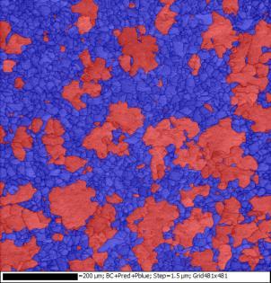
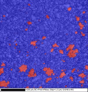
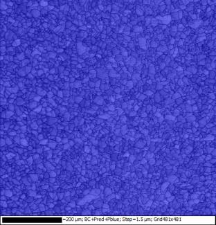
15 Example: Phase Transformation 945 o C 895 o C 0 mins 895 o C 6 mins 880 o C ferrite austenite
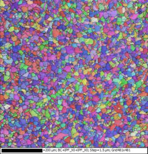
16 Automation with Flexibility Capability to automatically collect a data sequence to record changes in microstructure Adaptability to change acquisition conditions during the run This can be demonstrated using the following application example: An Al alloy application investigating both deformation and recrystallisation Load applied maps were acquired at regular intervals Load removed, sample heated up to 320 C sequence of maps collected


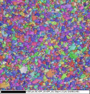
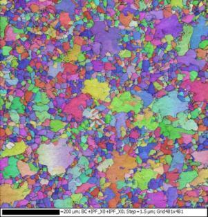
17 Al 0.1% Mg - Tensile Strain and Heating GATAN Microtest EH2000 Band Contrast Local mis-orientation IPF Isochronal heating 290, 300 and 320 o C Scattered pole figures (IPF colours)
 integrated IR filter Oxford Instruments AZtec platform flexibility ease of Use automation quality")
18 EBSD Solution The following application examples use: Oxford Instruments NordlysMax 2 fast detector (up to 870 Hz) integrated IR filter Oxford Instruments AZtec platform flexibility ease of Use automation quality data
19 In-situ Heating Characterisation Using EBSD Dr. Ali Gholinia Manchester University In-situ dynamic heating for Recrystallisation and Phase Transformation studies
20 Recrystallisation in Bronze and Steel Recrystallisation in Aluminium Phase transformation in Titanium Study of orientations in twin bands during phase transformation in Titanium


21 Before annealing After annealing Acknowledgements to Sylvia Campbell from MAHLE Engine Systems UK Ltd. for providing the Bronze samples.

22 IPF-X colour maps Thick black lines: High angle grain boundaries >10 Thin black lines: Low angle grain boundaries >2 Yellow lines: Twin boundaries Bronze Steel

23 Grains in random colours Thick black lines: High angle grain boundaries >10 Thin black lines: Low angle grain boundaries >2 Yellow lines: Twin boundaries Bronze Steel

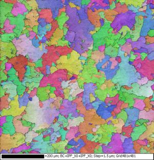
24 Recrystallisation in Aluminium Al-0.1Mg Band Contrast Harvinder Singh Ubhi et al., Materials Science Forum, V.753, (2013), p

25 Recrystallisation in Aluminium Al-0.1Mg Local misorientation


26 Recrystallisation in Aluminium Al-0.1Mg IPF-Z colours In-situ heating up to 295 C of deformed Al-0.1Mg alloy

27 Green: Ti-alpha (Hexagonal) Red: Ti-beta (Cubic) Acknowledgements to Jack Donoghue from University of Manchester for providing the Ti samples.


28 30 C Green: Ti-alpha (Hexagonal) Red: Ti-beta (Cubic) 20mm


29 200 C Green: Ti-alpha (Hexagonal) Red: Ti-beta (Cubic) 20mm


30 400 C Green: Ti-alpha (Hexagonal) Red: Ti-beta (Cubic) 20mm


31 600 C Green: Ti-alpha (Hexagonal) Red: Ti-beta (Cubic) 20mm


32 925 C Green: Ti-alpha (Hexagonal) Red: Ti-beta (Cubic) 20mm
 Red: Ti-beta")
33 950 C Green: Ti-alpha (Hexagonal) Red: Ti-beta (Cubic) 20mm
 Red: Ti-beta")
34 Green: Ti-alpha (Hexagonal) Red: Ti-beta (Cubic) 20mm
 Red: Ti-beta")
35 Green: Ti-alpha (Hexagonal) Red: Ti-beta (Cubic) 20mm
 Red: Ti-beta")
36 Green: Ti-alpha (Hexagonal) Red: Ti-beta (Cubic) 20mm
 Red: Ti-beta")
37 Green: Ti-alpha (Hexagonal) Red: Ti-beta (Cubic) 20mm
38 Green: Ti-alpha (Hexagonal) Red: Ti-beta (Cubic) 20mm
39 Conclusions In-situ dynamic heating allows the direct investigation of specific grains during recrystallisation and phase transformation. This enables the study of the order of recrystallisation of each grain and link the information to their microstructure. Phase transformation studies benefit from the knowledge of orientations at high temperatures and relating them to low temperatures. This direct link would not be possible in the conventional ex-situ static heating analysis. The free surface during in-situ heating may have some unknown effect on the microstructure development, however comparison of the ex-situ and in-situ microstructures have not shown significant differences.
40 In-situ Heating Characterisation Using EBSD Dr. Neil Othen Gatan UK
41 Heating Protection for the SEM The heating stage must offer good thermal isolation, water cooling and heat protection shields for use at high temperatures Precise temperature control. The stage must be responsive, but with a high level of accuracy so transformations can be controlled and observed Stability Minimal drift throughout heating. This can be achieved through a uniform heating platform with minimal thermal gradients and good thermal insulation.
42 Heating Size of the heating stage To be suitable for techniques such as EBSD a heating stage must be compact so it can be moved and tilted to the correct orientation Imaging At high temperatures, need to consider the limitations of SEM detectors and impact of thermal electrons. A bias voltage applied to the stage can improve imaging by reducing thermal electrons from the specimen Ease of use How quickly can the SEM be returned to normal operation? For multiuser facilities minimal delay in fitting removing the heating stages maximises time running samples
43 In-situ heating stage Gatan has developed a robust universal heating stage with a novel compact design suitable for: SED and EBSD imaging. Its optimum shape ensures full compatibility with EBSD whilst a choice of user changeable shields ensures protection to the SEM is maintained. The stage enables dynamic EBSD analysis of samples with a high temperature accuracy <0.5 C and stability <0.5 C per hour up to temperatures of 950 C. Suitable for specimens up to several mm 3 in size, a bulk specimens allows easier handling and avoids mis-interpretations due to thin films and surface artefacts.

44 In-situ heating stage The Gatan model 525 heating stage is specifically designed to suit in-situ market requirements Small, yet powerful, with high tilt compatibility giving optimum EBSD signal Precise controlled heating of specimens up to several mm 3 in size - crucial to observe stable transformations A detachable specimen holder provides quick sample exchange and storage Opportunity to prepare and mount specimens away from the SEM
45 Model 525 Murano heating stage System comprises:
46 Model 525 Murano heating stage System comprises: Water-cooled base attached to the SEM stage. Base is designed to suit individual SEMs and is easy to fit/remove. SEM stage can be returned to normal use within minutes. Water cooling with a safety interlock ensures protection for the SEM stage. No water - heating power to stage is stopped.

47 Model 525 Murano heating stage System comprises: A transferable heating specimen holder The holder fits on to the water cooled base, its dovetail design allows it to be loaded quickly and securely in under 1 minute The removable holder design allows the user to mount their specimen away from the SEM and store it if required for future work Allows airlock loading as a special option
48 Model 525 Murano heating stage System comprises: Consumable, heated specimen platform Specimen sits on centre platform and is secured using high temperature cement to ensure good thermal contact. The replaceable platform Prevents contamination between specimens. Allows individual specimen storage.


49 Model 525 Murano heating stage Consumable heated platform and loading jig allow multiple specimens to be prepared and stored.


50 SE imaging above 600 C PHOTO PENDING EBSD imaging above 600 C A choice of shielding options is available. Shield may be removed below 600 C


51 A programmable PC based temperature control provides flexibility for a range of experiments. Data logging and time stamping allows EBSD maps to be synchronise. 52

52 A compact design allows full SEM integration SEM FIB Heating stage EBSD No need for specimen re-mounting, as it is tilted from the 0 tilt loading position. Making it suitable for several analytical and imaging techniques.
53 Model 525 Murano in-situ heating stage Dynamic testing is possible in-situ in the SEM, with specifically designed heating stages. A more efficient workflow allows a single specimen to be used to study a complete temperature range. Specimens can be prepared, mounted and stored ready for use to allow quick SEM access
54 Summary EBSD coupled with in-situ dynamic heating is a powerful tool for studying microstructure in the SEM Offers an insight to material behaviour in use Modern analytical equipment makes acquiring this data a reality


55 Further reading Two in-situ EBSD application notes Tensile / Heating of Al 0.1% Mg Alloy In-situ EBSD Analysis of an Al Alloy
56 Q&A Dr. Ali Gholinia Dr. Neil Othen Dr. Jenny Goulden
Observation in the GB (Gentle Beam) Capabilities
 Capabilities") A field-emission cathode in the electron gun of a scanning electron microscope provides narrower probing beams at low as well as high electron energy, resulting in both improved spatial resolution and
A field-emission cathode in the electron gun of a scanning electron microscope provides narrower probing beams at low as well as high electron energy, resulting in both improved spatial resolution and
EBSD Basics EBSD. Marco Cantoni 021/ Centre Interdisciplinaire de Microscopie Electronique CIME. Phosphor Screen. Pole piece.
 EBSD Marco Cantoni 021/693.48.16 Centre Interdisciplinaire de Microscopie Electronique CIME EBSD Basics Quantitative, general microstructural characterization in the SEM Orientation measurements, phase
EBSD Electron BackScatter Diffraction Principle and Applications
 EBSD Electron BackScatter Diffraction Principle and Applications Dr. Emmanuelle Boehm-Courjault EPFL STI IMX Laboratoire de Simulation des Matériaux LSMX emmanuelle.boehm@epfl.ch 1 Outline! Introduction!
3D-EBSD an CrossBeam-Systemen
 FIB- Workshop 3.-4. July 2008 3D-EBSD an CrossBeam-Systemen Ulrike Zeile 1, Ali Gholinia 2 and Frank Bauer 3 Arbeitskreis FIB SSOM DGM/DGE ASEM Hotel Seeburg, Luzern, Switzerland 1. Carl Zeiss NTS 2. Oxford
Introduction to Electron Backscattered Diffraction. TEQIP Workshop HREXRD Feb 1 st to Feb 5 th 2016
 Introduction to Electron Backscattered Diffraction 1 TEQIP Workshop HREXRD Feb 1 st to Feb 5 th 2016 SE vs BSE 2 Ranges and interaction volumes 3 (1-2 m) http://www4.nau.edu/microanalysis/microprobe/interact-effects.html
AN EBSD STUDY OF THE MICRO STRUCTURAL DEVELOPMENT DURING ANNEALING OF A FOLDED SUPER DUPLEX STAINLESS STEEL SHEET SAMPLE.
 AN EBSD STUDY OF THE MICRO STRUCTURAL DEVELOPMENT DURING ANNEALING OF A FOLDED SUPER DUPLEX STAINLESS STEEL SHEET SAMPLE. H S Ubhi 1), J R Saithala 2) and H Jiang 1) 1) Oxford Instruments, High Wycombe.
Applications of EBSD
 Applications of EBSD Dr. V. Subramanya Sarma Department of Metallurgical and Materials Engineering Indian Institute of Technology Madras E-mail: vsarma@iitm.ac.in Applications of EBSD Grain size distribution
Carnegie Mellon MRSEC
 Carnegie Mellon MRSEC Texture, Microstructure & Anisotropy, Fall 2009 A.D. Rollett, P. Kalu 1 ELECTRONS SEM-based TEM-based Koseel ECP EBSD SADP Kikuchi Different types of microtexture techniques for obtaining
MODEL SEM Mill. Two independently adjustable TrueFocus ion sources
 MODEL 1060 SEM Mill A state-of-the-art ion milling and polishing system. It is compact, precise, and consistently produces high-quality scanning electron microscopy (SEM) samples for a wide variety of
NEMI Sn Whisker Modeling Group Part 2:Future Work
 NEMI Sn Whisker Modeling Group Part 2:Future Work IPC/NEMI Meeting Maureen Williams, NIST Irina Boguslavsky, NEMI Consultant November 7, 2002 New Orleans, LA Capabilities of NEMI Modeling Group NEMI Fundamental
In-situ Observation of Microstructure Change in Steel by EBSD
 NIPPON STEEL & SUMITOMO METAL TECHNICAL REPORT No. 114 MARCH 2017 Technical Report UDC 621. 785. 36 In-situ Observation of Microstructure Change in Steel by EBSD Masayuki WAKITA* Seiichi SUZUKI Abstract
FUSION IN SITU HEATING AND ELECTRICAL. Protochips Quantifiably Better
 FUSION IN SITU HEATING AND ELECTRICAL Protochips Quantifiably Better PtCo Nanoparticle 700 C Image courtesy Oak Ridge National Lab Fullerene STUDY MATERIALS 1200 C Image courtesy CIC nanogune WITH THERMAL
Electron channelling contrast imaging (ECCI) an amazing tool for observations of crystal lattice defects in bulk samples
 an amazing tool for observations of crystal lattice defects in bulk samples") Electron channelling contrast imaging (ECCI) an amazing tool for observations of crystal lattice defects in bulk samples Stefan Zaefferer with contributions of N. Elhami, (general & steels) Z. Li F. Ram,
Electron channelling contrast imaging (ECCI) an amazing tool for observations of crystal lattice defects in bulk samples Stefan Zaefferer with contributions of N. Elhami, (general & steels) Z. Li F. Ram,
Diffraction Contrast Tomography. Unlocking Crystallographic Information from Laboratory X-ray Microscopy. Technical Note
 Diffraction Contrast Tomography Unlocking Crystallographic Information from Laboratory X-ray Microscopy Technical Note Diffraction Contrast Tomography Unlocking Crystallographic Information from Laboratory
QUANTITATIVE MICROSTRUCTURE ANALYSIS OF DISPERSION STRENGTHENED Al-Al 4 C 3 MATERIAL BY EBSD TECHNIQUE
 Acta Metallurgica Slovaca, Vol. 16, 2010, No.2, p. 97-101 97 QUANTITATIVE MICROSTRUCTURE ANALYSIS OF DISPERSION STRENGTHENED Al-Al 4 C 3 MATERIAL BY EBSD TECHNIQUE M. Varchola, M. Besterci, K. Sülleiová
 LA-UR-01-3685 Approved for public release; distribution is unlimited. Title: USING A MULTI-DISCIPLINARY APPROACH, THE FIRST ELECTRON BACKSCATTERED KIKUCHI PATTERNS WERE CAPTURED FOR A PLUTONIUM ALLOY Author(s):
Thermo Scientific ARL EQUINOX X-ray Diffractometers
 Thermo Scientific ARL EQUINOX 1000 X-ray Diffractometers High performance in a compact size Thermo Scientific ARL EQUINOX 1000 X-ray diffractometer (XRD) is designed to meet structural and phase analysis
Development of bimodal grain structures in microalloyed steels:
 Development of bimodal grain structures in microalloyed steels: Niobium and titanium are added to high strength low alloy (HSLA) steels to provide grain boundary pinning precipitates to help produce the
Model TEM Mill. Tabletop precision preparation for producing high-quality TEM specimens from a wide variety of materials EXCELLENCE MAGNIFIED
 Model 1050 TEM Mill Tabletop precision preparation for producing high-quality TEM specimens from a wide variety of materials EXCELLENCE MAGNIFIED Modular design for basic instrument operation or fully
Texture Analysis in MSE
 Texture Analysis in MSE 집합조직제어연구실 서울대학교재료공학부 Texture (Preferred Orientation) Similarity of Texture E.T?! 한쪽을쳐다보고있는사람들여러방향을쳐다보는 Randomly Preferred Oriented What a Wonderful & Beautiful Life! Scientific
Rapid Imaging of Microstructure using Spatially Resolved Acoustic Spectroscopy
 Rapid Imaging of Microstructure using Spatially Resolved Acoustic Spectroscopy Steve Sharples, Matt Clark, Wenqi Li, Mike Somekh Applied Optics Group School of Electrical & Electronic Engineering University
ORIENTATION DETERMINATION BY EBSP IN AN ENVIRONMENTAL SCANNING ELECTRON MICROSCOPE
 Pergamon PII S1359-6462(99)00086-X Scripta Materialia, Vol. 41, No. 1, pp. 47 53, 1999 Elsevier Science Ltd Copyright 1999 Acta Metallurgica Inc. Printed in the USA. All rights reserved. 1359-6462/99/$
AN INTRODUCTION TO OIM ANALYSIS
 AN INTRODUCTION TO OIM ANALYSIS Raising the standard for EBSD software The most powerful, flexible, and easy to use tool for the visualization and analysis of EBSD mapping data OIM Analysis - The Standard
Thermo Scientific ARL EQUINOX 100. X-ray Diffractometers
 Thermo Scientific ARL EQUINOX 100 X-ray Diffractometers High performance in a compact size Thermo Scientific ARL EQUINOX 100 X-ray diffractometer (XRD) is designed to meet structural and phase analysis
Crystallographic Textures Measurement
 Crystallographic Textures Measurement D. V. Subramanya Sarma Department of Metallurgical and Materials Engineering Indian Institute of Technology Madras E-mail: vsarma@iitm.ac.in Macrotexture through pole
MODEL TEM Mill. Two independently adjustable TrueFocus ion sources
 MODEL 1050 TEM Mill A state-of-the-art ion milling and polishing system. It is compact, precise, and consistently produces high-quality transmission electron microscopy (TEM) specimens with large electron
Microstructural characterisation of as-deposited and reheated weld metal High Strength Steel Weld Metals
 Microstructural characterisation of as-deposited and reheated weld metal High Strength Steel Weld Metals Enda Keehan, Leif Karlsson, Mattias Thuvander, Eva-Lena Bergquist Abstract ESAB AB, Gothenburg,
Stuart I. Wright EDAX-TSL, Draper, Utah
 Stuart I. Wright EDAX-TSL, Draper, Utah EBSD Probably the Best Measurement in the World Austin Day, Microscopy & Microanalysis, 11, 502-503 (2005) OIM 3D Introduction to EBSD 3D Data Acquisition Serial
Practical 2P8 Transmission Electron Microscopy
 Practical 2P8 Transmission Electron Microscopy Originators: Dr. N.P. Young and Prof. J. M. Titchmarsh What you should learn from this practical Science This practical ties-in with the lecture course on
Practical 2P8 Transmission Electron Microscopy
 Practical 2P8 Transmission Electron Microscopy Originators: Dr. M. L. Jenkins and Prof. J. M. Titchmarsh What you should learn from this practical Science This practical ties-in with the lecture course
Microstructural Controls on Trace Element Variability in Ore Minerals
 2 Microstructural Controls on Trace Element Variability in Ore Minerals Question: Does EBSD provide new insight into ore mineral microstructure and the chemical enrichment of elements in hydrothermal ore
Grain Boundary Control for Improved Intergranular Stress Corrosion Cracking Resistance in Austenitic Stainless Steels
 Grain Boundary Control for Improved Intergranular Stress Corrosion Cracking Resistance in Austenitic Stainless Steels J MARROW, D ENGELBERG, A JIVKOV, P WOOD, L. BABOUT, N STEVENS Materials Performance
MODEL NanoMill TEM Specimen Preparation System. Ultra-low-energy, inert-gas ion source. Concentrated ion beam with scanning capabilities
 MODEL 1040 NanoMill TEM Specimen Preparation System The NanoMill system uses an ultra-low energy, concentrated ion beam to produce the highest quality specimens for transmission electron microscopy. Ultra-low-energy,
A Quantitative Evaluation of Microstructure by Electron Back-Scattered Diffraction Pattern Quality Variations
 Microsc. Microanal. 19, S5, 83 88, 2013 doi:10.1017/s1431927613012397 A Quantitative Evaluation of Microstructure by Electron Back-Scattered Diffraction Pattern Quality Variations SukHoonKang, 1 Hyung-Ha
JSM-7800F Field Emission Scanning Electron Microscope
 JSM-7800F catalogue JSM-7800F Field Emission Scanning Electron Microscope We provide high performance The Ultimate Research Tool for Multi-Disciplinary Research Institutions Extreme resolution The super
Low kv EBSD using AZtecHKL and NordlysNano: Characterisation of a mollusc shell
 Introduction Marine shells are of high interest to environmental sciences as they are excellent archives of past environmental change to geosciences as the fundamental material carrying the fossil record
Sr and Pb additions. L. Affleck, C. Leach *
 Microstructures of BaTiO 3 based PTC thermistors with Ca, Sr and Pb additions Abstract L. Affleck, C. Leach * Manchester Materials Science Centre University of Manchester and UMIST Grosvenor Street, Manchester
Liverpool, UK, L69 3GP
 Materials Science Forum Vols. 467-470 (2004) pp. 573-578 online at http://www.scientific.net 2004 Trans Tech Publications, Switzerland Using electron backscatter diffraction (EBSD) to measure misorientation
Recrystallization textures in metals and alloys
 Recrystallization textures in metals and alloys Uniaxial deformation Aluminium wire F.C.C. Metals and alloys FCC wires retain deformation texture ([111]+[100]) upon recrystallisation Composition / Purity
MICROSTRUCTURE AND TEXTURE
 Textures and Microstructures, Vol. 34, pp. 243-253 Reprints available directly from the publisher Photocopying permitted by license only (C) 2000 OPA (Overseas Publishers Association) N.V. Published by
Chapter 8: Strain Hardening and Annealing
 Slide 1 Chapter 8: Strain Hardening and Annealing 8-1 Slide 2 Learning Objectives 1. Relationship of cold working to the stress-strain curve 2. Strain-hardening mechanisms 3. Properties versus percent
Grain Contrast Imaging in UHV SLEEM
 Materials Transactions, Vol. 51, No. 2 (2010) pp. 292 to 296 Special Issue on Development and Fabrication of Advanced Materials Assisted by Nanotechnology and Microanalysis #2010 The Japan Institute of
Deformation and fracture of an alpha/beta titanium alloy
 ISSN 1517-7076 Revista Matéria, v. 15, n. 2, pp. 364-370, 2010. http://www.materia.coppe.ufrj.br/sarra/artigos/artigo11240 Deformation and fracture of an alpha/beta titanium alloy A. Andrade; A. Morcelli;
Empirical constraints of shock features in monazite using shocked zircon inclusions
 GSA Data Repository 2016205 Empirical constraints of shock features in monazite using shocked zircon inclusions Erickson et al. DR 1 Analytical methods Identification of Shocked Monazites and Imaging External
Application of Scanning Electron Microscope to Dislocation Imaging in Steel
 Application of Scanning Electron Microscope to Dislocation Imaging in Steel Masaaki Sugiyama and Masateru Shibata Advanced Technology Research Laboratories, Nippon Steel Corporation SM Business Unit, JEOL
ise J. A. Woollam Ellipsometry Solutions
 ise J. A. Woollam Ellipsometry Solutions Capabilities The ise is a new in-situ spectroscopic ellipsometer developed for real-time monitoring of thin film processing. Using our proven technology, the ise
Evolution of Microstructure and Texture Associated with Ridging in Ferritic Stainless Steels
 , pp. 100 105 Evolution of Microstructure and Texture Associated with Ridging in Ferritic Stainless Steels SooHo PARK, KwangYuk KIM, YongDeuk LEE and ChanGyung PARK 1) Stainless Steel Research Group, Technical
MiniFlex. Analysis of materials by X-ray diffraction. Benchtop XRD diffractometer
 MiniFlex Analysis of materials by X-ray diffraction Benchtop XRD diffractometer More power More flexibility More results The new MiniFlex is available in two models. The MiniFlex 600 is the most powerful
Study of the Initial Stage and an Anisotropic Growth of Oxide Layers Formed on Zircaloy-4
 16 th International Symposium on Zirconium in the Nuclear Industry, Chengdu, P. R. China, May 10-13, 2010 Study of the Initial Stage and an Anisotropic Growth of Oxide Layers Formed on Zircaloy-4 B. X.
Benchtop XRD diffractometer. MiniFlex. Analysis of materials by X-ray diffraction
 Benchtop XRD diffractometer MiniFlex Analysis of materials by X-ray diffraction More power More flexibility More results The new MiniFlex is available in two models. The MiniFlex 600 is the most powerful
MODEL 1061 SEM Mill ION MILLING. Ion milling is used in the physical. sciences to enhance the sample s surface. characteristics. Inert gas, typically
 MODEL 1061 SEM Mill A state-of-the-art ion milling and polishing system. It is compact, precise, and consistently produces high-quality scanning electron microscopy (SEM) samples in the shortest amount
Three stages: Annealing Textures. 1. Recovery 2. Recrystallisation most significant texture changes 3. Grain Growth
 Three stages: Annealing Textures 1. Recovery 2. Recrystallisation most significant texture changes 3. Grain Growth Cold worked 85% Cold worked 85% + stress relieved at 300 C for 1 hr Cold worked 85% +
Microtexture measurement of copper damascene line with EBSD
 Material Science Forum Vols. 408-412(2002) pp. 529-534 2002 Trans Tech Publications, Switzerland Microtexture measurement of copper damascene line with EBSD Dong-Ik Kim 1*, Jong-Min Paik 1, Young-Chang
MODEL PicoMill TEM specimen preparation system. Achieve ultimate specimen quality free from amorphous and implanted layers
 MODEL 1080 PicoMill TEM specimen preparation system Combines an ultra-low energy, inert gas ion source, and a scanning electron column with multiple detectors to yield optimal TEM specimens. POST-FIB PROCESSING
MICROSTRUCTURE CHARACTERIZATION OF GOES AFTER HOT ROLLING AND COLD ROLLING + DECARBURIZATION ANNEALING
 MICROSTRUCTURE CHARACTERIZATION OF GOES AFTER HOT ROLLING AND COLD ROLLING + DECARBURIZATION ANNEALING Vlastimil VODÁREK 1, Jan HOLEŠINSKÝ 1, Anastasia MASLOVA 1, František FILUŠ 1, Šárka MIKLUŠOVÁ 2,
Transzmissziós és pásztázó elektronmikroszkópos minták készítése ionsugaras vékonyítással
 Transzmissziós és pásztázó elektronmikroszkópos minták készítése ionsugaras vékonyítással Radi Zsolt Technoorg Linda Kft., Budapest Oktatói és Doktorandusz Konferencia Visegrád, 2012 State-of-the-art materials
Quantitative X-ray Microanalysis Of Submicron Carbide Formation In Chromium (III) Oxide Rich Scale
 Oxide Rich Scale") Quantitative X-ray Microanalysis Of Submicron Carbide Formation In Chromium (III) Oxide Rich Scale W. Keith Collins*, M. Ziomek-Moroz, G. R. Holcomb, P. Danielson, and A. Hunt *National Energy Technology
Quantitative X-ray Microanalysis Of Submicron Carbide Formation In Chromium (III) Oxide Rich Scale W. Keith Collins*, M. Ziomek-Moroz, G. R. Holcomb, P. Danielson, and A. Hunt *National Energy Technology
Electron Microscopy Studies of Niobium Thin Films on Copper
 Electron Microscopy Studies of Niobium Thin Films on Copper Roy Crooks 1, Greg Thompson 2, Robb Morris 2, Michelle Adams Hughes 3, Daudi Waryoba 3, and Peter Kalu 3 1 Black Laboratories, L.L.C., Newport
MODEL 1051 TEM Mill ION MILLING. Ion milling is used on physical science. specimens to reduce thickness to electron
 MODEL 1051 TEM Mill A state-of-the-art ion milling and polishing system offering reliable, high performance specimen preparation. It is compact, precise, and consistently produces high-quality transmission
John de Laeter Centre
 John de Laeter Centre Major research infrastructure hub at Curtin University, Perth, W.A. ~$30M worth of microscopes, spectrometers, diffractometers and experimental facilities AuScope partner, Microscopy
Exceptional Technology for Material Science TT DMA. Dynamic Mechanical Analyser
 Exceptional Technology for Material Science TT DMA Dynamic Mechanical Analyser The Company Triton Technology Ltd was first established in 1997 to design, manufacture and sell a range of instrumentation
Layer Thickness Analysis of Thin Metal Coatings with. Bruker Nano Analytics, Berlin, Germany Webinar, June 8 th 2017
 Layer Thickness Analysis of Thin Metal Coatings with micro-xrf on SEM Bruker Nano Analytics, Berlin, Germany Webinar, June 8 th 2017 09.06.2017 Presenters Stephan Boehm Product Manager Micro-XRF/SEM Bruker
Development of a Reconstruction Method of Prior Austenite Microstructure Using EBSD Data of Martensite
 Technical Report UDC 621. 785. 36 Development of a Reconstruction Method of Prior Austenite Microstructure Using EBSD Data of Martensite Kengo HATA* Kazuki FUJIWARA Masayuki WAKITA Kaori KAWANO Abstract
COMPARISON OF TEXTURE IN COPPER AND ALUMINUM THIN FILMS DETERMINED BY XRD AND EBSD *
 COMPARISON OF TEXTURE IN COPPER AND ALUMINUM THIN FILMS DETERMINED BY XRD AND EBSD * 201 J. Müller 1, D. Balzar 1,2, R.H. Geiss 1, D.T. Read 1, and R.R. Keller 1 1 Materials Reliability Division, National
ATTACHMENTES FOR EXPLORER DIFFRACTOMETER. Monochromators
 Monochromators Secondary flat and curved graphite monochromators suitable for Ag, Cr, Fe, Cu, Co and Mo radiations This attachment is installed in the X-ray detection unit. It is designed to remove continuous
ATTACHMENTES FOR APD 2000 PRO POWDER X-RAY DIFFRACTOMETER. Monochromators
 Monochromators Secondary graphite monochromator Johansson Ka 1 monochromator Parabolic monochromator Secondary flat and curved graphite monochromators suitable for Ag, Cr, Fe, Cu, Co and Mo radiations
Combining Measurement Methods The Benefit of Fast Analytical Instruments
 Combining Measurement Methods The Benefit of Fast Analytical Instruments Jana Bergholtz, Daniel Goran, Stephan Boehm, René Chemnitzer Bruker Nano GmbH, Berlin, Webinar, October 25 th, 2012 Innovation with
CHAPTER 4: The wetting behaviour and reaction of the diamond-si system
 CHAPTER 4: The wetting behaviour and reaction of the diamond-si system In this chapter, the wetting behaviour of diamond by silicon will be presented, followed by the study of the interaction between diamond
Transmission Kikuchi Diffraction in the Scanning Electron Microscope
 Transmission Kikuchi Diffraction in the Scanning Electron Microscope Robert Keller, Roy Geiss, Katherine Rice National Institute of Standards and Technology Nanoscale Reliability Group Boulder, Colorado
Tutorial 2 : Crystalline Solid, Solidification, Crystal Defect and Diffusion
 Tutorial 1 : Introduction and Atomic Bonding 1. Explain the difference between ionic and metallic bonding between atoms in engineering materials. 2. Show that the atomic packing factor for Face Centred
On-axis Transmission Kikuchi Diffraction in the SEM. Performances and Applications
 On-axis Transmission Kikuchi Diffraction in the SEM. Performances and Applications Etienne Brodu, Emmanuel Bouzy, Jean-Jacques Fundenberger Séminaire «les microscopies électroniques à Metz et à Nancy»
Additive manufacturing
 Comparison Between Microstructures, Deformation Mechanisms and Micromechanical Properties of 316L Stainless Steel Consolidated by Laser Melting I. Heikkilä, O. Karlsson, D. Lindell, A. Angré, Y. Zhong,
Experimental and theoretical investigation of the microstructural evolution in aluminium alloys during extrusion
 Computational Methods and Experiments in Materials Characterisation IV 209 Experimental and theoretical investigation of the microstructural evolution in aluminium alloys during extrusion T. Kayser, F.
CHAPTER FOUR METALLIC SUBSTRATES
 CHAPTER FOUR METALLIC SUBSTRATES This chapter falls broadly into two parts. Firstly the preparation of textured metallic substrates is described with emphasis on the degree of crystallographic alignment.
In situ SEM observation of electromigration phenomena in fully embedded copper interconnect structures
 Microelectronic Engineering 64 (2002) 375 382 www.elsevier.com/ locate/ mee In situ SEM observation of electromigration phenomena in fully embedded copper interconnect structures Abstract M.A. Meyer *,
Finding Grain and Antigrains. Matt Nowell May 2016
 Finding Grain and Antigrains Matt Nowell May 2016 1 Grains Grain Boundaries Grain Size Measurements Special Boundaries Grain Shape Antigrains Outline Acknowledgements Stuart Wright, Rene de Kloe (EDAX),
In Situ Observation of Dislocation Nucleation and Escape in a Submicron Al Single Crystal
 Supplementary Information for In Situ Observation of Dislocation Nucleation and Escape in a Submicron Al Single Crystal Sang Ho Oh*, Marc Legros, Daniel Kiener and Gerhard Dehm *To whom correspondence
Transmission Kikuchi Diffraction in the Scanning Electron Microscope
 in the Scanning Electron Microscope Robert Keller, NIST, Boulder, USA Daniel Goran, Bruker Nano, Berlin, Germany 24 th April 2013 Innovation with Integrity in the Scanning Electron Microscope Robert Keller,
Mambo is the perfect tool for viewing EBSD data in pole and inverse pole figures.
 Mambo Pole figure and inverse pole figure software The physical properties of many samples are dependent on the common alignment of particular crystallographic directions: one of the easiest ways to view
Trust but verify: Ensure product quality at all stages of production
 QUALITY Trust but verify: Ensure product quality at all stages of production TRUST BUT The tool of choice for manufacturing Quality Control and Assurance To prevent product failures and their costly consequences
The X-MET8000 is great when you need accurate on-site alloy identification and chemistry in metal recycling and scrap yards.
 RECYCLING The is great when you need accurate on-site alloy identification and chemistry in metal recycling and scrap yards. The optimised combination of a high performance X-ray tube and large area silicon-drift
Evolution of Recrystallization Texture in Aluminum Alloy Sheets by Asymmetric-Warm-Rolling
 技術論文 Evolution of Recrystallization Texture in Aluminum Alloy Sheets by Asymmetric-Warm-Rolling Yoshikazu Suzuki Osamu Noguchi Yoshiki Miki Yoichi Ueno Katsumi Koyama Toshio Komatsubara Abstract : Asymmetric-warm-rolling
IMP EPD End Point Detector
 IMP EPD End Point Detector An overview of the Hiden Analytical SIMS end point detector system for ion beam etch applications IMP-EPD Presentation Topics The topics covered in the presentation include:
Electron backscattered diffraction study of poly-si by Ni-mediated crystallization of amorphous silicon using a SiO 2 nanocap
 Electron backscattered diffraction study of poly-si by Ni-mediated crystallization of amorphous silicon using a SiO 2 nanocap Y. J. Chang, a) J. H. Oh, K. H. Kim, and Jin Jang b) Advanced Display Research
ELECTRON BACKSCATTER DIFFRACTION (EBSD) THE METHOD AND ITS APPLICATIONS IN MATERIALS SCIENCE AND ENGINEERING
 THE METHOD AND ITS APPLICATIONS IN MATERIALS SCIENCE AND ENGINEERING") ELECTRON BACKSCATTER DIFFRACTION (EBSD) THE METHOD AND ITS APPLICATIONS IN MATERIALS SCIENCE AND ENGINEERING P. Cizek UNIVERSITY OF OXFORD, Department of Materials, Parks Road, Oxford OX1 3PH, GB Abstract
ELECTRON BACKSCATTER DIFFRACTION (EBSD) THE METHOD AND ITS APPLICATIONS IN MATERIALS SCIENCE AND ENGINEERING P. Cizek UNIVERSITY OF OXFORD, Department of Materials, Parks Road, Oxford OX1 3PH, GB Abstract
Combined EBSD & EDS analysis: Advances in modern materials characterization
 Combined EBSD & EDS analysis: Advances in modern materials characterization Gert Nolze, Bruker Nano, Berlin EBSD/EDS Webinar, April 6 th, 2011 Innovation with Integrity Talk outline QUANTAX CrystAlign
Workshop of Electron backscatter diffraction (EBSD) in Scanning Electron Microscope
 in Scanning Electron Microscope") Workshop of Electron backscatter diffraction (EBSD) in Scanning Electron Microscope 12 13 July 2017 School of Physics, Universiti Sains Malaysia Electron backscatter diffraction (EBSD) in scanning electron
Workshop of Electron backscatter diffraction (EBSD) in Scanning Electron Microscope 12 13 July 2017 School of Physics, Universiti Sains Malaysia Electron backscatter diffraction (EBSD) in scanning electron
X-MET8000 Series. Sort scrap metal accurately, fast and maximise profits
 Sort scrap metal accurately, fast and maximise profits SCRAP Regional Distributor: Eastern Applied Research, Inc. Ph: 716-201-1115 ~ Em: sales@easternapplied.com ETALS Maximise sorting throughput and improve
Wavelength Dispersive XRF Spectrometer
 ISO9001 ISO14001 for Wafers, Media Disks, and Large Samples Wavelength Dispersive XRF Spectrometer ADVANCED XRF For Large and Irregularly Shaped Samples Is there any solution to analyze a large sample
Workshop of Electron backscatter diffraction (EBSD) in Scanning Electron Microscope
 in Scanning Electron Microscope") Workshop of Electron backscatter diffraction (EBSD) in Scanning Electron Microscope 12 13 July 2017 School of Physics, Universiti Sains Malaysia Electron backscatter diffraction (EBSD) in scanning electron
Workshop of Electron backscatter diffraction (EBSD) in Scanning Electron Microscope 12 13 July 2017 School of Physics, Universiti Sains Malaysia Electron backscatter diffraction (EBSD) in scanning electron
1P1b: Introduction to Microscopy
 1P1b: Introduction to Microscopy Central to the study and characterisation of metals and many other materials is the microscope, ranging from the magnification of, say, 1 to 35 in a simple stereo binocular
Evaluation of Solidification Cracking Susceptibility for Austenitic Stainless Steel during Laser Trans-Varestraint Test Using Twodimensional
 ISIJ International, Vol. 56 (2016), ISIJ International, No. 11 Vol. 56 (2016), No. 11, pp. 2022 2028 Evaluation of Solidification Cracking Susceptibility for Austenitic Stainless Steel during Laser Trans-Varestraint
Microstructural and Textural Evolution by Continuous Cyclic Bending and Annealing in a High Purity Titanium
 Materials Transactions, Vol. 45, No. 9 (24) pp. 2826 to 2831 #24 The Japan Institute of Metals Microstructural and Textural Evolution by Continuous Cyclic Bending and Annealing in a High Purity Titanium
Mathematical Modelling of an Annealing Furnace for Process Control Applications
 Mathematical Modelling of an Annealing Furnace for Process Control Applications N.Depree 1, J.Sneyd 2, S.Taylor 2, M.P.Taylor 1, M.O Connor 3, J.J.J.Chen 4 1 Light Metals Research Centre, University of
The Study of SEM Examination of Crept Ceramic Samples Prepared by Cross Polishing Method
 The Study of SEM Examination of Crept Ceramic Samples Prepared by Cross Polishing Method Alper Uludag Faculty of Aeronautics and Astronautics Anadolu University Eskisehir, Turkey alperuludag@anadolu.edu.tr
The use of holographic optics in laser additive layer manufacture. Prof John R Tyrer Dept of Mechanical & Manufacturing Engineering
 The use of holographic optics in laser additive layer manufacture Prof John R Tyrer Dept of Mechanical & Manufacturing Engineering Traditional Laser Beam Problems Shape Intensity Beam intensity distribution....
Focused Ion Beam CENTRE INTERDISCIPLINAIRE DE MICROSCOPIE ELECTRONIQUE. Marco Cantoni, EPFL-CIME CIME ASSEMBLEE GENERALE 2007
 Focused Ion Beam @ CENTRE INTERDISCIPLINAIRE DE MICROSCOPIE ELECTRONIQUE Present situation and vision Marco Cantoni, EPFL-CIME Dual Beam Nova 600 Nanolab from FEI Company FE-SEM & FIB: Ga LMIS 4 Gas Injector
Microstructure of Friction Stir Welded 6061 Aluminum Alloy
 Proceedings of the 9 th International Conference on Aluminium Alloys (2004) Edited by J.F. Nie, A.J. Morton and B.C. Muddle Institute of Materials Engineering Australasia Ltd 878 Microstructure of Friction
Study on Estimation Methods of Applied Stress using Fractography Analysis
 156 Study on Estimation Methods of Applied Stress using Fractography Analysis Hideaki Kaneko* 1 Hiroshi Ishikawa* 1 Takashi Konishi* 1 Masahiro Yamada* 1 The damage mode and applied stress must be estimated