IMP EPD End Point Detector
|
|
|
- Brian Weaver
- 6 years ago
- Views:
Transcription

1 IMP EPD End Point Detector An overview of the Hiden Analytical SIMS end point detector system for ion beam etch applications
2 IMP-EPD Presentation Topics The topics covered in the presentation include: A description of the Hiden IMP end point detector system Example data Hardware and software Integration with process tools

3 Hiden IMP EPD The Hiden IMP EPD is used for the precise end point detection in the ion beam etch step of the fabrication of thin film devices The Hiden IMP is a differentially pumped, ruggedized secondary ion mass spectrometer for the analysis of secondary ions and neutrals from the ion beam etch process
4 The IMP EPD system comprises: Stainless Steel Shroud with Sampling Orifice IMP-EPD Ion Optics with Energy Analyser and integral ioniser Triple filter Quadrupole mass analyser Pulse Ion Counting Detector Differentially Pumped Manifold With Mounting Flange to Process Chamber Data System with integration to the process tool


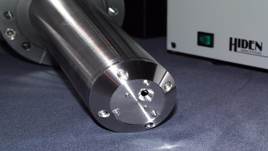
5 IMP-EPD Photo courtesy of:

6 Inside a typical ion beam etch chamber IMP- EPD Analyser Photo and Diagram courtesy of EPFL
7 End Point Detection Mask Mask Material A Mat. A Substrate Mat. B Substrate Mat. B Primary Ion Beam Secondary Ions Mat. A Secondary Ions Mat. B

8 IMP EPD end point data The data from the IMP end point detector provides a trend analysis for each component of the etch stack. The trend analysis provides a real time display of the entire etch process. The etch resolution combined with the sensitivity of the SIMS technique provides for end point detection to within +/- 5Å. The signals for each layer of the stack materials are coupled with algorithms and data I/O interfaces to provide for automated end point for a broad range of etch end point criteria including rising and falling edge.

9 Data Output Each peak corresponds to a layer. Each colour corresponds to a metal or other element. A wide peak corresponds to a thick layer When you etch through a layer the signal goes up.
10 Signal collection

11 Front end detail
12 Angle of acceptance b a +/- 5deg ~50% of signal Relative angular acceptance
13 Example data - 30 Angstrom Tantalum Layers Ta / NiFe /Ta Tantulum SEM : c/s Nickel :00 03:20 06:40 10:00 13:20 16:40 20:00 Time MM:SS The IMP EPD data shows the depth resolution achieved in an ion mill of a: tantalum / nickel iron / tantalum stack where the tantalum layers are 30 Angstroms.
14 Example Data Multilayered Sample: FeMn/NiFe/Co/Cu/Co/NiFe/Ta Data Zoom Iron Copper SEM : c/s 1000 Manganese Cobalt 100 Nickel Tantalum 10 00:00 01:40 03:20 05:00 06:40 08:20 10:00 11:40 13:20 15:00 Time MM:SS
15 Data Zoom in showing signal variation due to wafer rotation Multilayered Sample: FeMn/NiFe/Co/Cu/Co/NiFe/Ta Iron Copper SEM : c/s Manganese Cobalt Nickel Tantalum 0 04:50 05:10 05:30 05:50 06:10 06:30 06:50 07:10 07:30 07:50 08:10 Time MM:SS

16 4 Wafers run sequentially: Wafer number 3 has an imperfection recorded The data shows the consistency of analysis in production. Tantalum, Nickel and Silicon are monitored. The third wafer has an imperfection in the recorded silicon signal.
17 IMP EPD Materials Guide- SIMS analyses all elements dopants and clusters INTERFACE Si/Ga Au/Cr/Al Au/Ti/Ga Mo/Ge Al/In Al/Ga Y/Ba/Cu/MgO NiCr/Cu/NiFe/SiO2 APPLICATION EXAMPLE Identification of SiO2 interface on III-V semiconductor. Au/Cr track identification on aluminium substrates. Precise definition of Au/Ti electrical contacts in GaAs. Precise definition of Mo/Ge interfaces in multifilm Mo/Ge structures. Identification of the interface between two semiconductors Al In As/InP. To etch down to the interface between two layers of AlGaAs separated by a 79 Å GaAs well. The Al signal clearly identified the sandwich. Identification of separate layers in multilayer superconductor materials. Magnetic disc sensor head manufacture.
18 Layer Mass to monitor Mass number AlTiC Ti 48 CoFe Co 59 Al 2 O 3 Al / AlO 27 / 43 Mass Channels For Layer Materials Ta Ta 181 NiFe Ni 58 Cu Cu 63 FeMn Mn 55 Co Co 59 Ca Ca 40 Ti Ti 48 Cr Cr 52 Ag Ag 107 Au Au 197 Pt Pt 195 Si Si / SiO 28 / 44
19 Process Variables that affect angle of acceptance include: Wafer tilt The IMP end point detector probe operates over a wide range of wafer tilt angles Surface roughness Primary ion beam energy The sensitivity of the Hiden IMP-EPD is sufficient to provide end point control on 99.9% masked wafers.
20 End Point Control The end point is controlled with the following criteria: Rising edge or Falling edge with variables: Mass channel Percentage over etch Timed over etch Time out over etch
21 End Point Control Parameters Endpoint detection is based on a falling or rising trend in the signal; signal intensities and change rates must be entered into the endpoint template for the EPD to operate correctly. Values are needed for the initial delay, slope, limit, falling, % fall, over-etch-time, and % over-etch parameters, which are defined as follows: Initial-delay The delay, in seconds, after the start of the run until end-point detection is enabled. This may be used to ensure endpoint detection ignores any layers above the endpoint layer. slope limit falling Minimum slope value for the rising edge of the endpoint layer. This value is the minimum difference required between the signals read in the current and previous (normally 5 cycles earlier) scan cycles before a trace maximum (and, therefore, an endpoint) will be detected. A suitable value for this parameter can compensate for noise or sample rotation. A minimum intensity limit for the endpoint layer. Signals below this level are regarded as noise or background and are not used for endpoint detection. Set true (1) if the endpoint is to be a falling edge, otherwise set false (0). Falling edge detection is recommended as it allows a level relative to the layer maximum to be used (see % fall). % fall Determines how far below the maximum the signal must fall before the endpoint is signalled. over-etch The time, in seconds, after the endpoint is detected before the endpoint signal is set true. Determines time how long the etc continues after the endpoint. % over-etch Over-etch time as a percentage of the run time. This is the delay after the endpoint is detected before the endpoint signal is set true. It can compensate for varying etch rates. max_over The maximum time, in seconds, that a percentage over-etch may take. This time will not be exceeded etch even if a calculated percentage over-etch time is longer.
22 IMP EPD end point control HAL4 PP-EPD #10620 SEM : c/s Endpoint ion signal 100% %fall limit 0 00:00 00:10 00:20 00:30 00:40 00:50 01:00 01:10 01:20 01:30 01:40 Time mm:ss L1/L3 L2 Substrate Start Endpoint set clear set clear initial-delay over-etch-time or %over-etch Normal endpoint max_over-etch Endpoint set clear Endpoint where max_over-etch time exceeded
23 The IMP provides End Point Control- What else does the IMP do? Target Impurity Determination At the start of the etch the ion milling probe provides high sensitivity SIMS spectra for the identification of impurities from surface and primary ion source contamination Residual Gas Analysis The integral electron impact ioniser of the IMP allows for operation as a conventional differentially pumped RGA, with software control for leak detection and gas analysis included


24 Hiden IMP-EPD users The IMP EPD was developed in the 1980 s for researchers working on new devices based on thin film technology. The research devices of the 1990 s have become full production applications. The 2007 Nobel Prize in Physics was awarded to Albert Fert and Peter Grünberg for the discovery of the Giant magnetoresistance GMR effect. The IMP-EPD is currently in use 24/7 for production of HDD read/write heads based on GMR technology at Seagate, Western Digital, Toshiba and Hitachi Global Storage. The IMP-EPD is currently used in the development of the next generation of devices at the worlds leading research centres including:
25 Summary IMP EPD for end point detection in ion beam etch processes: End Point resolution; +/- 5 Angstroms IMP-EPD Sensitivity sufficient to work with 99.9% masked wafers Sensitivity sufficient to work with small samples from 6mm 2 to large scale. Process control for production Adaptable to large and small ion beam etch chambers Operates as a residual gas analyzer, RGA
Advanced Sensor Fabrication Using Integrated Ion Beam Etch and Ion Beam Deposition Processes
 Advanced Sensor Fabrication Using Integrated Ion Beam Etch and Ion Beam Deposition Processes Jhon F. Londoño, Kurt E. Williams, Adrian J. Devasahayam Veeco Instruments Inc. Plainview, New York U.S.A Figure
Differentially pumped quadrupole SIMS probe on FIBbased and two-beam microscopes
 Differentially pumped quadrupole SIMS probe on FIBbased and two-beam microscopes Richard J Chater (1), Barbara Shollock (1), David McPhail (1), Alan J Smith (2) and Graham Cooke (2) (1) Department of Materials,
Precision Without Compromise
 D1 EVOLUTION Precision Without Compromise Versatile and user-friendly high resolution and multipurpose X-ray diffractometer for the characterization of advanced materials www.jvsemi.com D1 Overview Introduction
Wavelength Dispersive XRF Spectrometer
 ISO9001 ISO14001 for Wafers, Media Disks, and Large Samples Wavelength Dispersive XRF Spectrometer ADVANCED XRF For Large and Irregularly Shaped Samples Is there any solution to analyze a large sample
Specimen Preparation Technique for a Microstructure Analysis Using the Focused Ion Beam Process
 Specimen Preparation Technique for a Microstructure Analysis Using the Focused Ion Beam Process by Kozue Yabusaki * and Hirokazu Sasaki * In recent years the FIB technique has been widely used for specimen
In-Situ Low-Angle Cross Sectioning: Bevel Slope Flattening due to Self-Alignment Effects
 In-Situ Low-Angle Cross Sectioning: Bevel Slope Flattening due to Self-Alignment Effects UWE SCHEITHAUER SIEMENS AG, CT MM 7, Otto-Hahn-Ring 6, 81739 München, Germany Phone: + 49 89 636 44143 E-mail: uwe.scheithauer@siemens.com
A discussion of crystal growth, lithography, etching, doping, and device structures is presented in
 Chapter 5 PROCESSING OF DEVICES A discussion of crystal growth, lithography, etching, doping, and device structures is presented in the following overview gures. SEMICONDUCTOR DEVICE PROCESSING: AN OVERVIEW
RIX3100. Fully Automated Sequential X-ray Spectrometer System. Product Information
 The Rigaku Journal Vol. 14/ number 1/ 1997 Product Information Fully Automated Sequential X-ray Spectrometer System RIX3100 1. Introduction Wavelength dispersive X-ray fluorescence (WDXRF) analysis methods
High-Energy Resolution Microcalorimeter EDS System for Electron Beam Excitation
 High-Energy Resolution Microcalorimeter EDS System for Electron Beam Excitation *K. Tanaka, A. Nagata, N. Sasayama, M. Ikeda, A. Odawara, S. Nakayama and K. Chinone. SII NanoTechnology Inc.,563 Takatsuka-shinden,
Layer Thickness Analysis of Thin Metal Coatings with. Bruker Nano Analytics, Berlin, Germany Webinar, June 8 th 2017
 Layer Thickness Analysis of Thin Metal Coatings with micro-xrf on SEM Bruker Nano Analytics, Berlin, Germany Webinar, June 8 th 2017 09.06.2017 Presenters Stephan Boehm Product Manager Micro-XRF/SEM Bruker
INA-X System for SNMS and SIMS
 Customized Systems and Solutions Nanostructures and Thin Film Deposition Surface Analysis and Preparation Components Surface Science Application INA-X System for SNMS and SIMS Application Notes The quantitative
X-RAY DIFFRACTION IN SEMICONDUCTOR INDUSTRY AND RESEARCH
 X-RAY DIFFRACTION IN SEMICONDUCTOR INDUSTRY AND RESEARCH M. Leszczyński High Pressure Research Center UNIPRESS, Sokolowska 29/37, 01 142 Warsaw, Poland, e-mail: mike@unipress.waw.pl ABSTRACT The paper
2008 Summer School on Spin Transfer Torque
 2008 Summer School on Spin Transfer Torque Nano-scale device fabrication 2-July-2008 Byoung-Chul Min Center for Spintronics Research Korea Institute of Science and Technology Introduction Moore s Law
2006 UPDATE METROLOGY
 INTERNATIONAL TECHNOLOGY ROADMAP FOR SEMICONDUCTORS METROLOGY THE ITRS DEVED AND INTENDED FOR TECHNOLOGY ASSESSMENT ONLY AND WITHOUT REGARD TO ANY COMMERCIAL CONSIDERATIONS PERTAINING TO INDIVIDUAL PRODUCTS
In-line Hybrid Metrology Solutions
 In-line Hybrid Metrology Solutions Brad Lawrence Regional Sales & Product Marketing Manager, XwinSys ED-XRF Based Metrology with Hybrid Sensor Technology Hybrid Sensor In-Line Metrology Process feedback
Chapter 4 Fabrication Process of Silicon Carrier and. Gold-Gold Thermocompression Bonding
 Chapter 4 Fabrication Process of Silicon Carrier and Gold-Gold Thermocompression Bonding 4.1 Introduction As mentioned in chapter 2, the MEMs carrier is designed to integrate the micro-machined inductor
ise J. A. Woollam Ellipsometry Solutions
 ise J. A. Woollam Ellipsometry Solutions Capabilities The ise is a new in-situ spectroscopic ellipsometer developed for real-time monitoring of thin film processing. Using our proven technology, the ise
S. Gupta. The University of Alabama
 Overview of Sputtering Technologies for Thin-Film Head Applications S. Gupta Associate Professor Dept. of Metallurgical and Materials Engineering Collaborators and Sponsors This work was supported in part
Electrodeposition of Magnetic Materials
 Electrodeposition of Magnetic Materials Neil Robertson HGST, a Western Digital Company San Jose Research Center San Jose, California Electrodeposition and the HDD Business HDD s are a very high volume
Sputtering Targets for Microelectronics. Sputtering Targets for Semiconductor Applications
 Sputtering Targets for Microelectronics Sputtering Targets for Semiconductor Applications Umicore Thin Film Products Umicore Thin Film Products, a globally active business unit within the Umicore Group,
Lecture 5. SOI Micromachining. SOI MUMPs. SOI Micromachining. Silicon-on-Insulator Microstructures. Agenda:
 EEL6935 Advanced MEMS (Spring 2005) Instructor: Dr. Huikai Xie SOI Micromachining Agenda: SOI Micromachining SOI MUMPs Multi-level structures Lecture 5 Silicon-on-Insulator Microstructures Single-crystal
Oxidation behavior of Cu nanoclusters in hybrid thin films
 Oxidation behavior of Cu nanoclusters in hybrid thin films Harm Wulff,* Steffen Drache*, Vitezslav Stranak**, Angela Kruth*** *EMAU Greifswald, **South Bohemian University, Budweis, *** INP Greifswald
We get small. Micron-scale Circuits and Structures from Prototype through Production
 We get small. Micron-scale Circuits and Structures from Prototype through Production Smaller, tighter, better. When you need to produce ultra-small electrical, mechanical and optical components to extreme
METHOD FOR IMPROVING FIB PREPARED TEM SAMPLES BY VERY LOW ENERGY Ar + ION MILL POLISHING
 METHOD FOR IMPROVING FIB PREPARED TEM SAMPLES BY VERY LOW ENERGY Ar + ION MILL POLISHING Yaron Kauffmann, Tzipi Cohen-Hyams, Michael Kalina, Hila Sadan-Meltzman and Wayne D. Kaplan Dept. of Materials Engineering
Advanced Materials Analysis with Micro-XRF for SEM
 Advanced Materials Analysis with Micro-XRF for SEM Birgit Hansen, Application Scientist EDS and Micro-XRF for SEM Stephan Boehm, Product Manager Micro-XRF for SEM Bruker Nano GmbH, Berlin, Germany Innovation
Thin Film Gas Sensor. Nanoelectronics and MEMS Laboratory National Electronics and Computer Technology
 Ion-assisted E-beam E Evaporated Thin Film Gas Sensor A. Wisitsoraat,, A. A Tuantranont,, V. V Patthanasettakul, T. Lomas,, and P. Chindaudom Nanoelectronics and MEMS Laboratory National Electronics and
SUB-Programs - Calibration range Fe Base for "PMI-MASTER Pro" Spark - mode Fe 000
 SUB-Programs - Calibration range Fe Base for "PMI-MASTER Pro" Spark - mode Fe 100 Fe 200 *** Fe 250 *** Fe 300 Fe 400 Fe 500 Fe 000 Fe low alloy steel cast iron Cr hard / Ni resist stainless steel tool
Why Probes Look the Way They Do Concepts and Technologies of AFM Probes Manufacturing
 Agilent Technologies AFM e-seminar: Understanding and Choosing the Correct Cantilever for Your Application Oliver Krause NanoWorld Services GmbH All mentioned company names and trademarks are property
In-situ Heating Characterisation Using EBSD
 Webinar In-situ Heating Characterisation Using EBSD Speakers Dr. Ali Gholinia Dr. Neil Othen Dr. Jenny Goulden Topics Introduction to EBSD Why do in-situ experiments? EBSD equipment requirements for in-situ
Lecture Day 2 Deposition
 Deposition Lecture Day 2 Deposition PVD - Physical Vapor Deposition E-beam Evaporation Thermal Evaporation (wire feed vs boat) Sputtering CVD - Chemical Vapor Deposition PECVD LPCVD MVD ALD MBE Plating
Fabrication Process. Crystal Growth Doping Deposition Patterning Lithography Oxidation Ion Implementation CONCORDIA VLSI DESIGN LAB
 Fabrication Process Crystal Growth Doping Deposition Patterning Lithography Oxidation Ion Implementation 1 Fabrication- CMOS Process Starting Material Preparation 1. Produce Metallurgical Grade Silicon
Chapter 1.6. Polished Single-Crystal Silicon, Prime Wafers (all numbers nominal) Wafer Specification Table. Diameter 100 mm 4-inch 150 mm 6-inch
 Wafer Specification Table. Diameter 100 mm 4-inch 150 mm 6-inch") Chapter 1.6 I - Substrate Specifications Polished Single-Crystal Silicon, Prime Wafers (all numbers nominal) Wafer Specification Table Diameter 100 mm 4-inch 150 mm 6-inch Thickness 525 µm 20.5 mils 675
Chapter 1.6 I - Substrate Specifications Polished Single-Crystal Silicon, Prime Wafers (all numbers nominal) Wafer Specification Table Diameter 100 mm 4-inch 150 mm 6-inch Thickness 525 µm 20.5 mils 675
Activities in Plasma Process Technology at SENTECH Instruments GmbH, Berlin. Dr. Frank Schmidt
 Activities in Plasma Process Technology at SENTECH Instruments GmbH, Berlin Dr. Frank Schmidt The Company Company Private company, founded 1990 80 employees ISO 9001 Location Science & Technology Park,
GDMS. High Resolution GDMS.
 GDMS astrum ES High Resolution GDMS www.nu-ins.com Astrum ES Glow discharge mass spectrometry (GD-MS) is recognised as one of the ultimate techniques for the characterisation of conductive and non-conductive
COMPATIBILITY OF THE ALTERNATIVE SEED LAYER (ASL) PROCESS WITH MONO- Si AND POLY-Si SUBSTRATES PATTERNED BY LASER OR WET ETCHING
 PROCESS WITH MONO- Si AND POLY-Si SUBSTRATES PATTERNED BY LASER OR WET ETCHING") COMPATIBILITY OF THE ALTERNATIVE SEED LAYER (ASL) PROCESS WITH MONO- Si AND POLY-Si SUBSTRATES PATTERNED BY LASER OR WET ETCHING Lynne Michaelson 1, Anh Viet Nguyen 2, Krystal Munoz 1, Jonathan C. Wang
COMPATIBILITY OF THE ALTERNATIVE SEED LAYER (ASL) PROCESS WITH MONO- Si AND POLY-Si SUBSTRATES PATTERNED BY LASER OR WET ETCHING Lynne Michaelson 1, Anh Viet Nguyen 2, Krystal Munoz 1, Jonathan C. Wang
S8 TIGER Series 2. Lab Report XRF 144. Innovation with Integrity. Accurate Quality Control of Tool Steels XRF
 Lab Report XRF 144 S8 TIGER Series 2 Accurate Quality Control of Tool Steels Tool steels are iron-based alloys that are particularly well-suited to be made into tools. Their suitability comes from their
h Reclamation Center Lot Number List
 h Reclamation Center Lot Number List Lot #Description Base Metal Primary PM 0 Mixed Material and Computers Mixed 1 IC device w/encapsulation, plastic - Malaysia Copper Gold 2 IC device w/encapsulation,
General Introduction to Microstructure Technology p. 1 What is Microstructure Technology? p. 1 From Microstructure Technology to Microsystems
 General Introduction to Microstructure Technology p. 1 What is Microstructure Technology? p. 1 From Microstructure Technology to Microsystems Technology p. 9 The Parallels to Microelectronics p. 15 The
SUPPLEMENTARY INFORMATIONS
 SUPPLEMENTARY INFORMATIONS Dynamic Evolution of Conducting Nanofilament in Resistive Switching Memories Jui-Yuan Chen, Cheng-Lun Hsin,,, Chun-Wei Huang, Chung-Hua Chiu, Yu-Ting Huang, Su-Jien Lin, Wen-Wei
1 MARCH 2017 FILM DEPOSITION NANOTECHNOLOGY
 1 MARCH 2017 FILM DEPOSITION NANOTECHNOLOGY PRESENTATION Pedro C. Feijoo E-mail: PedroCarlos.Feijoo@uab.cat FABRICATION TECHNOLOGIES FOR NANOELECTRONIC DEVICES. PEDRO C. FEIJOO 2 FILM GROWTH Chemical vapor
Development of different copper seed layers with respect to the copper electroplating process
 Microelectronic Engineering 50 (2000) 433 440 www.elsevier.nl/ locate/ mee Development of different copper seed layers with respect to the copper electroplating process a, a a b b b K. Weiss *, S. Riedel,
Acoustic Characterization of Materials
 Acoustic Characterization of Materials Bernhard R. Tittmann Group Leader CAV Introduction Graduate Students 4 Ph.D. Candidates 4 U.S. 1 Non-US 3 M.S Candidates 3 U.S. 1 Non U.S. Visiting Scholars Dr.
Platypus Gold Coated Substrates. Bringing Science to the Surface
 Platypus Gold Coated Substrates Bringing Science to the Surface Overview Gold Coated Substrates - Gold Coating Introduction - Glossary of Terms - Gold Coating Methods - Critical Features Platypus Gold
Advanced Analytical Techniques for Semiconductor Assembly Materials and Processes. Jason Chou and Sze Pei Lim Indium Corporation
 Advanced Analytical Techniques for Semiconductor Assembly Materials and Processes Jason Chou and Sze Pei Lim Indium Corporation Agenda Company introduction Semiconductor assembly roadmap challenges Fine
Supporting Information
 Supporting Information Fast-Response, Sensitivitive and Low-Powered Chemosensors by Fusing Nanostructured Porous Thin Film and IDEs-Microheater Chip Zhengfei Dai,, Lei Xu,#,, Guotao Duan *,, Tie Li *,,
Nanoscale Imaging, Material Removal and Deposition for Fabrication of Cutting-edge Semiconductor Devices
 Hitachi Review Vol. 65 (2016), No. 7 233 Featured Articles Nanoscale Imaging, Material Removal and Deposition for Fabrication of Cutting-edge Semiconductor Devices Ion-beam-based Photomask Defect Repair
SEMASPEC Test Method for Metallurgical Analysis for Gas Distribution System Components
 SEMASPEC Test Method for Metallurgical Analysis for Gas Distribution System Components Technology Transfer 91060574B-STD and the logo are registered service marks of, Inc. 1996, Inc. SEMASPEC Test Method
In operandi observation of dynamic annealing: a case. Supplementary Material
 In operandi observation of dynamic annealing: a case study of boron in germanium nanowire devices Supplementary Material Maria M. Koleśnik-Gray, 1,3,4 Christian Sorger, 1 Subhajit Biswas, 2,3 Justin D.
Epitaxy and Roughness Study of Glancing Angle Deposited Nanoarrays. Hamid Alouach and G. J. Mankey
 Epitaxy and Roughness Study of Glancing Angle Deposited Nanoarrays Hamid Alouach and G. J. Mankey Introduction Objective: Approach: Characterization: Fabrication of nanoscale magnetic wires for spin transport
Electrical and Fluidic Microbumps and Interconnects for 3D-IC and Silicon Interposer
 Electrical and Fluidic Microbumps and Interconnects for 3D-IC and Silicon Interposer Li Zheng, Student Member, IEEE, and Muhannad S. Bakir, Senior Member, IEEE Georgia Institute of Technology Atlanta,
Introduction to CMOS VLSI Design. Layout, Fabrication, and Elementary Logic Design
 Introduction to CMOS VLSI Design Layout, Fabrication, and Elementary Logic Design CMOS Fabrication CMOS transistors are fabricated on silicon wafer Lithography process similar to printing press On each
FRONT END PROCESSES - CLEANING, LITHOGRAPHY, OXIDATION ION IMPLANTATION, DIFFUSION, DEPOSITION AND ETCHING
 Manufacturing, Cleaning, Gettering - Chapter 4 FRONT END PROCESSES - CLEANING, LITHOGRAPHY, OXIDATION ION IMPLANTATION, DIFFUSION, DEPOSITION AND ETCHING Over the next several weeks, we ll study front
Oerlikon PVD production solutions for piezoelectric materials
 Oerlikon PVD production solutions for piezoelectric materials Workshop PiezoMEMS Aachen,18. /19.05.2010 M. Kratzer Oerlikon Systems R&D Oerlikon company and products Thin films used for SAW, BAW, MEMS,
Perpendicular Magnetic Multilayers for Advanced Memory Application
 Perpendicular Magnetic Multilayers for Advanced Memory Application Sangmun Oh; Zheng Gao Kochan Ju; Lijie Guan HGST Wafer Development Team 2012 HGST, a Western Digital company 2012 HGST, a Western Digital
Physical Vapor Deposition (PVD) Zheng Yang
 Zheng Yang") Physical Vapor Deposition (PVD) Zheng Yang ERF 3017, email: yangzhen@uic.edu Page 1 Major Fabrication Steps in MOS Process Flow UV light Mask oxygen Silicon dioxide photoresist exposed photoresist oxide
Physical Vapor Deposition (PVD) Zheng Yang ERF 3017, email: yangzhen@uic.edu Page 1 Major Fabrication Steps in MOS Process Flow UV light Mask oxygen Silicon dioxide photoresist exposed photoresist oxide
Microanalysis with high spectral resolution: the power of QUANTAX WDS for SEM
 Microanalysis with high spectral resolution: the power of QUANTAX WDS for SEM Bruker Nano Analytics, Berlin, Germany Webinar, September 14, 2017 Innovation with Integrity Presenters Dr. Jörg Silbermann
Today s Class. Materials for MEMS
 Lecture 2: VLSI-based Fabrication for MEMS: Fundamentals Prasanna S. Gandhi Assistant Professor, Department of Mechanical Engineering, Indian Institute of Technology, Bombay, Recap: Last Class What is
Atomic Layer Deposition (ALD)
") Atomic Layer Deposition (ALD) ALD provides Uniform, controlled, conformal deposition of oxide, nitride, and metal thin films on a nanometer scale. ALD is a self limiting thin film deposition technique
Atomic Layer Deposition (ALD) ALD provides Uniform, controlled, conformal deposition of oxide, nitride, and metal thin films on a nanometer scale. ALD is a self limiting thin film deposition technique
Progress in Monolithic III-V/Si and towards processing III-V Devices in Silicon Manufacturing. E.A. (Gene) Fitzgerald
 Fitzgerald") Progress in Monolithic III-V/Si and towards processing III-V Devices in Silicon Manufacturing E.A. (Gene) Fitzgerald M.J. Mori, C.L.Dohrman, K. Chilukuri MIT Cambridge, MA USA Funding: MARCO IFC and Army
Progress in Monolithic III-V/Si and towards processing III-V Devices in Silicon Manufacturing E.A. (Gene) Fitzgerald M.J. Mori, C.L.Dohrman, K. Chilukuri MIT Cambridge, MA USA Funding: MARCO IFC and Army
Plasma Quest Limited
 Plasma Quest Limited A Remote Plasma Sputter Process for High Rate Web Coating of Low Temperature Plastic Film with High Quality Thin Film Metals and Insulators Dr. Peter Hockley and Prof. Mike Thwaites,
1. Scope :- 2. Referenced Documents :-
 Standard Specification for Forged or Rolled N06030, N06022, N06035, N06200, N06059, N06686, N08020, N08024, N 08026, N08367, N10276, N10665, N10675, N 10629, N08031, N06045, N06025, and R20033 Alloy Pipe
The Physical Structure (NMOS)
") The Physical Structure (NMOS) Al SiO2 Field Oxide Gate oxide S n+ Polysilicon Gate Al SiO2 SiO2 D n+ L channel P Substrate Field Oxide contact Metal (S) n+ (G) L W n+ (D) Poly 1 3D Perspective 2 3 Fabrication
The Physical Structure (NMOS) Al SiO2 Field Oxide Gate oxide S n+ Polysilicon Gate Al SiO2 SiO2 D n+ L channel P Substrate Field Oxide contact Metal (S) n+ (G) L W n+ (D) Poly 1 3D Perspective 2 3 Fabrication
Precision Micro-Aperture Catalog
 National Aperture, Inc. Precision Micro-Aperture Catalog Version 2009-1 PLEASE CONTACT: Dan Gentile Sales Associate, National Aperture, Inc. Telephone: (603) 893-7393, (800) 360-4598, Fax: (603) 893-7857
National Nano Fabrication Centre (NNFC)
") National Nano Fabrication Centre (NNFC) Tool and Process Capabilities 1. Lithography 1.1 Direct Laser Writer/Lithography 1.1.1 Preferred Design file format: GDS2 or CIF 1.1.2 Please note that coloured
National Nano Fabrication Centre (NNFC) Tool and Process Capabilities 1. Lithography 1.1 Direct Laser Writer/Lithography 1.1.1 Preferred Design file format: GDS2 or CIF 1.1.2 Please note that coloured
Transzmissziós és pásztázó elektronmikroszkópos minták készítése ionsugaras vékonyítással
 Transzmissziós és pásztázó elektronmikroszkópos minták készítése ionsugaras vékonyítással Radi Zsolt Technoorg Linda Kft., Budapest Oktatói és Doktorandusz Konferencia Visegrád, 2012 State-of-the-art materials
Thermal Evaporation. Theory
 Thermal Evaporation Theory 1. Introduction Procedures for depositing films are a very important set of processes since all of the layers above the surface of the wafer must be deposited. We can classify
CMOS Fabrication. Dr. Bassam Jamil. Adopted from slides of the textbook
 CMOS Fabrication Dr. Bassam Jamil Adopted from slides of the textbook CMOS Fabrication CMOS transistors are fabricated on silicon wafer Lithography process similar to printing press On each step, different
Quantitative X-ray Microanalysis Of Submicron Carbide Formation In Chromium (III) Oxide Rich Scale
 Oxide Rich Scale") Quantitative X-ray Microanalysis Of Submicron Carbide Formation In Chromium (III) Oxide Rich Scale W. Keith Collins*, M. Ziomek-Moroz, G. R. Holcomb, P. Danielson, and A. Hunt *National Energy Technology
Quantitative X-ray Microanalysis Of Submicron Carbide Formation In Chromium (III) Oxide Rich Scale W. Keith Collins*, M. Ziomek-Moroz, G. R. Holcomb, P. Danielson, and A. Hunt *National Energy Technology
HIGH SPATIAL RESOLUTION AND HIGH ENERGY RESOLUTION AUGER DEPTH PROFILING
 Application Note HIGH SPATIAL RESOLUTION AND HIGH ENERGY RESOLUTION AUGER DEPTH PROFILING of / Films OVERVIEW The formation processes of nickel silicide thin films are of particular interest for sub-65
Chapter 3 Silicon Device Fabrication Technology
 Chapter 3 Silicon Device Fabrication Technology Over 10 15 transistors (or 100,000 for every person in the world) are manufactured every year. VLSI (Very Large Scale Integration) ULSI (Ultra Large Scale
Title Ta, and Au for 28.8 MeV Alpha Parti. Author(s) Ishiwari, Ryutaro; Shiomi, Naoko; S.
 Ishiwari, Ryutaro; Shiomi, Naoko; S.") Title Stopping Powers of Be, Al, Ti, V, F Ta, and Au for 28.8 MeV Alpha Parti Author(s) Ishiwari, Ryutaro; Shiomi, Naoko; S Citation Bulletin of the Institute for Chemi University (1977), 55(1): 60-67
Title Stopping Powers of Be, Al, Ti, V, F Ta, and Au for 28.8 MeV Alpha Parti Author(s) Ishiwari, Ryutaro; Shiomi, Naoko; S Citation Bulletin of the Institute for Chemi University (1977), 55(1): 60-67
Direct Analysis of Photoresist by ICP-MS. Featuring the Agilent Technologies 7500s ICP-MS
 Direct Analysis of Photoresist by ICP-MS Featuring the Agilent Technologies 7500s ICP-MS 1 Presentation Outline How is photoresist used? Analytical challenges Instrumentation developments Analytical approach
Analysis of steel and its alloys using the GB/T standard and an Agilent 5100 ICP-OES in dual view mode
 Analysis of steel and its alloys using the GB/T 20125-2006 standard and an Agilent 5100 ICP-OES in dual view mode Application note Metals analysis and production Authors John Cauduro Agilent Technologies
Overview of CMP for TSV Applications. Robert L. Rhoades, Ph.D. Presentation for AVS Joint Meeting June 2013 San Jose, CA
 Overview of CMP for TSV Applications Robert L. Rhoades, Ph.D. Presentation for AVS Joint Meeting June 2013 San Jose, CA Outline TSV s and the Role of CMP TSV Pattern and Fill TSV Reveal (non-selective)
Electron Beam Induced Processes and their Applicability to Mask Repair
 & Electron Beam Induced Processes and their Applicability to Mask Repair Hans W.P. Koops (1), Volker Boegli (1), Klaus Edinger (1), Johannes Bihr (2), Jens Greiser (2), (1) NaWoTec GmbH Rossdorf Germany
EECS130 Integrated Circuit Devices
 EECS130 Integrated Circuit Devices Professor Ali Javey 9/13/2007 Fabrication Technology Lecture 1 Silicon Device Fabrication Technology Over 10 15 transistors (or 100,000 for every person in the world)
the surface of a wafer, usually silicone. In this process, an oxidizing agent diffuses into the wafer
 Analysis of Oxide Thickness Measurement Techniques of SiO2: Nanometrics Nanospec Reflectometer and Color Chart Eman Mousa Alhajji North Carolina State University Department of Materials Science and Engineering
STRUCTURAL ANALYSIS OF TSVS
 STRUCTURAL ANALYSIS OF TSVS HUGO BENDER CHRIS DRIJBOOMS, PATRICIA VAN MARCKE, JEF GEYPEN, OLIVIER RICHARD, PAOLA FAVIA EFUG2010 Gaeta, 11 October 2010 OUTLINE Introduction : 3D device stacking FIB analysis
Application of sprayed carbon nanotubes to light detectors
 Olive Tree (St. Nicholas Church in Bari) Application of sprayed carbon nanotubes to light detectors Valentini A. (1)(2), Melisi D. (1), Valentini M. (1), Nitti M.A. (2), Biagi P.F. (2) (1) INFN Sezione
MODEL PicoMill TEM specimen preparation system. Achieve ultimate specimen quality free from amorphous and implanted layers
 MODEL 1080 PicoMill TEM specimen preparation system Combines an ultra-low energy, inert gas ion source, and a scanning electron column with multiple detectors to yield optimal TEM specimens. POST-FIB PROCESSING
Recent Progress on LAPPD
 Recent Progress on LAPPD Andrey Elagin University of Chicago NNN 2016, IHEP, Beijing, November 5, 2016 Outline LAPPD Overview Commercialization status at Incom Inc. R&D Towards Volume Production - development
1 nanometer can be the difference ELECTRONICS COATINGS XRF ANALYZERS
 1 nanometer can be the difference ELECTRONICS COATINGS XRF ANALYZERS 1 nanometre can be the difference Drawing on our 40 years experience of providing coatings analysis solutions to a range of industries,
Chapter 4: Imperfections (Defects) in Solids
 in Solids") Chapter 4: Imperfections (Defects) in Solids ISSUES TO ADDRESS... What types of defects exist in solids? How do defects affect material properties? Can the number and type of defects be varied and controlled?
Chapter 4: Imperfections (Defects) in Solids ISSUES TO ADDRESS... What types of defects exist in solids? How do defects affect material properties? Can the number and type of defects be varied and controlled?
Characterization of Surface Metals on Silicon Wafers by SME-ICP-MS. Featuring the Agilent Technologies 7500s ICP-MS
 Characterization of Surface Metals on Silicon Wafers by SME-ICP-MS Featuring the Agilent Technologies 7500s ICP-MS 1 Presentation Outline Why is Surface Metal Extraction ICP-MS important? Technique Wafer
Analysis of Copper and Copper Base Alloys, Using Shimadzu PDA-7000
 C112-0514M Analysis of Copper and Copper Base Alloys, Using Shimadzu PDA-7000 Copper alloys are designated by their chemical composition with characteristic properties such as high corrosion resistance,
Effects of Thin Film Depositions on the EUV mask Flatness
 Effects of Thin Film Depositions on the EUV mask Flatness Kyoung-Yoon Bang, Jinback Back, Hwan-Seok Seo, Dongwan Kim, DongHoon Chung, SeongSue Kim, Sang-Gyun Woo, and HanKu Cho Photomask Team Semiconductor
Fundamentals of X-ray diffraction and scattering
 Fundamentals of X-ray diffraction and scattering Don Savage dsavage@wisc.edu 1231 Engineering Research Building (608) 263-0831 X-ray diffraction and X-ray scattering Involves the elastic scattering of
Synchrotron X-Ray Topography Measurements on 4H-SiC Epitaxial Layer
 Synchrotron X-Ray Topography Measurements on 4H-SiC Epitaxial Layer Isaho KAMATA, Central Research Institute of Electric Power Industry (CRIEPI) Kamata@criepi.denken.or.jp Silicon carbide has excellent
UT Austin, ECE Department VLSI Design 2. CMOS Fabrication, Layout Rules
 2. CMOS Fabrication, Layout, Design Rules Last module: Introduction to the course How a transistor works CMOS transistors This module: CMOS Fabrication Design Rules CMOS Fabrication CMOS transistors are
CERTIFIED REFERENCE MATERIALS (CRM)
") CERTIFIED REFERENCE MATERIALS (CRM) Sufficiently Homogenized Indian Reference Materials certified by Round robin analysis for the use of validation of methods and calibration. CSIR-National Metallurgical
CERTIFIED REFERENCE MATERIALS (CRM) Sufficiently Homogenized Indian Reference Materials certified by Round robin analysis for the use of validation of methods and calibration. CSIR-National Metallurgical
Analysis of inhomogeneous samples and trace element detection in alloys using QUANTAX Micro-XRF on SEM
 Analysis of inhomogeneous samples and trace element detection in alloys using QUANTAX Micro-XRF on SEM Bruker Nano Analytics, Berlin, Germany Webinar, June 02, 2016 Innovation with Integrity Presenters
What s Hot in Heat Assisted Magnetic Recording (HAMR)
") What s Hot in Heat Assisted Magnetic Recording (HAMR) Mark Re Senior Vice President Seagate Research Some of this work was performed as part of the Information Storage Industry Consortium (INSIC) program
What s Hot in Heat Assisted Magnetic Recording (HAMR) Mark Re Senior Vice President Seagate Research Some of this work was performed as part of the Information Storage Industry Consortium (INSIC) program
JSM-7800F Field Emission Scanning Electron Microscope
 JSM-7800F catalogue JSM-7800F Field Emission Scanning Electron Microscope We provide high performance The Ultimate Research Tool for Multi-Disciplinary Research Institutions Extreme resolution The super
Improving coupling coefficient distribution on BAW filters manufactured on 200mm wafers
 Improving coupling coefficient distribution on BAW filters manufactured on 200mm wafers Sergey Mishin Advanced Modular Systems, Inc Goleta, CA/USA smishin@amssb.com Yury Oshmyansky Advanced Modular Systems,
A New Development to Eliminate Artifacts during TEM Sample Preparation in the FIB
 Inspire Innovation Through Collaboration High Technologies America, Inc. A New Development to Eliminate Artifacts during TEM Sample Preparation in the FIB (Un)traditional FIB Preparation A Common Problem
Applications. SIMS successfully applied to many fields. Catalysts, metals, ceramics, minerals may primarily use imaging
 Applications SIMS successfully applied to many fields Catalysts, metals, ceramics, minerals may primarily use imaging Semiconductors extensively use depth profiling Si, GaAs, GaN, ZnO Minerals Analysis
Alloy Steels. Engineering Materials. Introduction : Msc. Shaymaa Mahmood
 Alloy Steels Introduction : Steels are, essentially, alloys of iron and carbon, containing up to 1.5 % of carbon. Steel is made by oxidizing away the impurities that are present in the iron produced in
Managing Anode Effects and Substrate Heating from Rotatable Sputter Targets
 Managing Anode Effects and Substrate Heating from Rotatable Sputter Targets Frank Papa*, Dermot Monaghan**, Victor Bellido- González**, and Alex Azzopardi** *Gencoa Technical & Business Support in US,
O2 Plasma Damage and Dielectric Recoveries to Patterned CDO Low-k Dielectrics
 O2 Plasma Damage and Dielectric Recoveries to Patterned CDO Low-k Dielectrics H. Huang 1, J. Bao 1, H. Shi 1, P. S. Ho 1, M L McSwiney 2, M D Goodner 2, M Moinpour 2, and G M Kloster 2 1 Laboratory for
Performance, Reliability, and Versatility. Transpector CPM. Fast, Field-ready Process Monitoring System
 Performance, Reliability, and Versatility Transpector CPM Fast, Field-ready Process Monitoring System Precision measurement for modern semiconductor processes INFICON Transpector CPM has been the films.